ICGOO在线商城 > 集成电路(IC) > PMIC - 栅极驱动器 > RT9624AZS

 Datasheet下载
- 型号: RT9624AZS
- 制造商: RICHTEK
- 库位|库存: xxxx|xxxx
- 要求:
| 数量阶梯 | 香港交货 | 国内含税 |
| +xxxx | $xxxx | ¥xxxx |
查看当月历史价格
查看今年历史价格
RT9624AZS产品简介:
ICGOO电子元器件商城为您提供RT9624AZS由RICHTEK设计生产,在icgoo商城现货销售,并且可以通过原厂、代理商等渠道进行代购。 RT9624AZS价格参考。RICHTEKRT9624AZS封装/规格:PMIC - 栅极驱动器, Half-Bridge Gate Driver IC Inverting, Non-Inverting 8-SOP。您可以下载RT9624AZS参考资料、Datasheet数据手册功能说明书,资料中有RT9624AZS 详细功能的应用电路图电压和使用方法及教程。
RT9624AZS 是由 Richtek USA Inc.(立锜科技)生产的一款电源管理集成电路(PMIC),具体分类为栅极驱动器(Gate Driver)。该器件主要用于驱动功率MOSFET或IGBT等开关器件,常见于需要高效功率转换的应用场合。

主要应用场景包括:

1. DC-DC转换器:适用于同步整流降压(Buck)或升压(Boost)转换器,为功率MOSFET提供高效栅极驱动,提高转换效率。

2. 电机驱动系统:在直流电机或步进电机控制电路中,用于驱动H桥结构中的功率管,实现电机正反转及调速。

3. 电源管理系统:应用于服务器电源、通信电源、工业电源等高可靠性系统中,作为功率开关的驱动控制单元。

4. LED照明驱动:在高功率LED驱动电路中,用于控制开关管,实现恒流输出和高效率工作。

5. 电池管理系统(BMS):在电池充放电管理电路中,用于控制充放电通路中的功率MOSFET。

RT9624AZS具备高驱动能力、低传输延迟、宽工作电压范围等特性,适合中高功率应用。其封装形式为TSOT,适用于紧凑型设计,广泛应用于工业控制、通信设备、消费电子等领域。
| 参数 | 数值 |
| 产品目录 | 集成电路 (IC) |
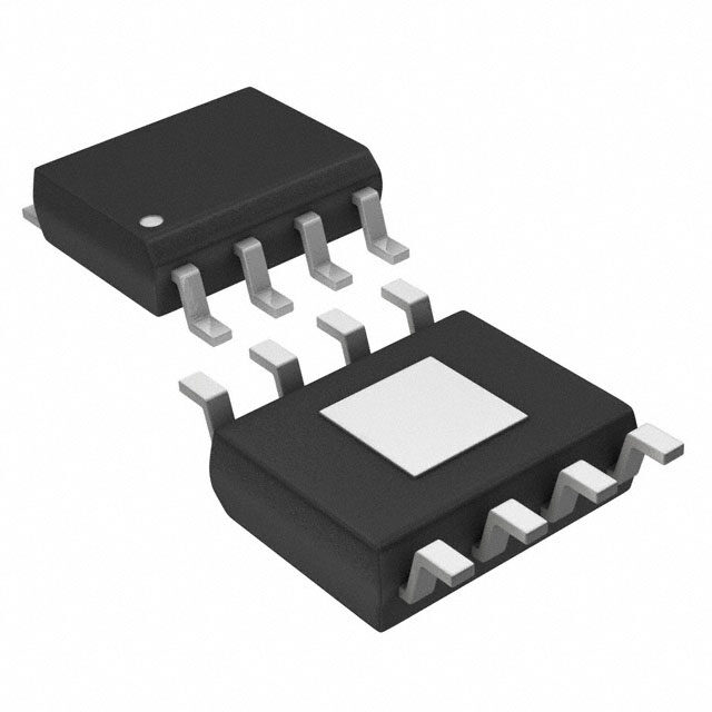
| 描述 | IC FET DVR 1CH SYNC BUCK 8SOP |
| 产品分类 | PMIC - MOSFET,电桥驱动器 - 外部开关 |
| 品牌 | Richtek USA Inc |
| 数据手册 | http://www.richtek.com/download_ds.jsp?s=854 |
| 产品图片 |
|
| 产品型号 | RT9624AZS |
| rohs | 无铅 / 符合限制有害物质指令(RoHS)规范要求 |
| RoHS指令信息 | http://www.richtek.com/download.jsp?t=UyUyRmFzc2V0cyUyRjIwMDklMkYwNiUyRjE3JTJGcGFnZTY1MTYwenRpeGIucGRmJTNEJTNEJTNE%0AR0w5NTI1LUMtLVBiLWZyZWUrUHJvZHVjdCsrR3JlZW4rUHJvZHVjdCtTdGF0ZW1lbnQrMDkwNjE2%0AQw%3D%3D |
| 产品系列 | - |
| 供应商器件封装 | 8-SOP |
| 其它名称 | 1028-1229-1 |
| 包装 | 剪切带 (CT) |
| 安装类型 | 表面贴装 |
| 封装/外壳 | 8-SOIC(0.154",3.90mm 宽) |
| 工作温度 | -40°C ~ 85°C |
| 延迟时间 | 30ns |
| 标准包装 | 1 |
| 电压-电源 | 4.5 V ~ 13.2 V |
| 电流-峰值 | - |
| 输入类型 | PWM |
| 输出数 | 2 |
| 配置 | 高端和低端,同步 |
| 配置数 | 1 |
| 高压侧电压-最大值(自举) | - |


PDF Datasheet 数据手册内容提取
® RT9624A Single Phase Synchronous Rectified Buck MOSFET Driver General Description Features The RT9624A is a high frequency, synchronous rectified, Drive Two N-MOSFETs single phase MOSFET driver designed for normal MOSFET Shoot Through Protection driving applications and high performance CPU VR driving Embedded Bootstrap Diode capabilities. Support High Switching Frequency Fast Output Rising Time The RT9624A can be supplied from 4.5V to 13.2V. The Tri-State PWM Input for Output Shutdown applicable power stage VIN range is from 5V to 24V. The Enable Control RT9624A also builds in an internal power switch to replace Small SOP-8, SOP-8 (Exposed Pad) and 8-Lead external bootstrap diode. WDFN Packages The RT9624A can support switching frequency efficiently RoHS Compliant and Halogen Free up to 500kHz. The RT9624A has both the UGATE and LGATE driving circuits for synchronous rectified DC/DC Applications converter applications. The shoot through protection mechanism is designed to prevent shoot through between Core Voltage Supplies for Desktop, Motherboard CPU high side and low side power MOSFETs. The RT9624A High Frequency Low Profile DC/DC Converters has tri-state PWM input with shutdown and EN input High Current Low Voltage DC/DC Converters shutdown functions, which can force driver to output low Core Voltage Supplies for GFX Card UGATE and LGATE signals. The RT9624A comes in a small footprint with 8-pin packages. The choice of package types includes SOP-8, SOP-8 (Exposed Pad) and WDFN-8L 3x3. Simplified Application Circuit RT9624A VIN R1 R2 12V VCC BOOT C5 C6 C1 CBOOT UGATE Q1 R3 L1 Chip Enable EN PHASE VOUT + R5 PWM R4 C3 C4 PWM LGATE Q2 Controller C2 GND Copyright © 2015 Richtek Technology Corporation. All rights reserved. is a registered trademark of Richtek Technology Corporation. DS9624A-07 July 2015 www.richtek.com 1
RT9624A Ordering Information Pin Configurations RT9624A (TOP VIEW) Package Type BOOT 8 UGATE S : SOP-8 PWM 2 7 PHASE SP : SOP-8 (Exposed Pad-Option1) EN 3 6 GND QW : WDFN-8L 3x3 (W-Type) VCC 4 5 LGATE Lead Plating System SOP-8 Z : ECO (Ecological Element with Halogen Free and Pb free) BOOT 8 UGATE Note : PWM 2 7 PHASE Richtek products are : GND EN 3 6 GND 9 RoHS compliant and compatible with the current require- VCC 4 5 LGATE ments of IPC/JEDEC J-STD-020. SOP-8 (Exposed Pad) Suitable for use in SnPb or Pb-free soldering processes. BOOT 1 8 UGATE PWM 2 D 7 PHASE Marking Information N EN 3 G 6 GND VCC 4 9 5 LGATE RT9624AZS RT9624AZS : Product Number WDFN-8L 3x3 RT9624A YMDNN : Date Code ZSYMDNN RT9624AZSP RT9624AZSP : Product Number RT9624A YMDNN : Date Code ZSPYMDNN RT9624AZQW 00 : Product Code 00 YM YMDNN : Date Code DNN Copyright © 2015 Richtek Technology Corporation. All rights reserved. is a registered trademark of Richtek Technology Corporation. www.richtek.com DS9624A-07 July 2015 2
RT9624A Function Pin Description Pin No. Pin Name Pin Function SOP-8 (Exposed Pad) / SOP-8 WDFN-8L 3x3 1 1 BOOT Bootstrap Supply for High Side Gate Drive. PWM Signal Input. Connect this pin to the PWM output of the 2 2 PWM controller. Chip Enable (Active High). When this pin is low, both UGATE 3 3 EN and LGATE are driven to low. 4 4 VCC Supply Voltage Input. Low Side Gate Driver Output. Connect this pin to the Gate of 5 5 LGATE low side power N-MOSFET. 6, Ground. The exposed pad must be soldered to a large PCB 6 GND 9 (Exposed Pad) and connected to GND for maximum power dissipation. Connect this pin to the Source of the high side N-MOSFET 7 7 PHASE and the Drain of the low side N-MOSFET. High Side Gate Drive Output. Connect this pin to the Gate of 8 8 UGATE high side power N-MOSFET. Function Block Diagram EN VCC Bootstrap Enable POR Control Detect Internal BOOT VDD Shoot-Through UGATE Protection Tri-State PWM Detect Turn Off PHASE Detection VCC Shoot-Through LGATE Protection GND Copyright © 2015 Richtek Technology Corporation. All rights reserved. is a registered trademark of Richtek Technology Corporation. DS9624A-07 July 2015 www.richtek.com 3
RT9624A Operation POR (Power On Reset) Bootstrap Control POR block detects the voltage the VCC pin. When the Bootstrap control block controls the integrated bootstrap VCC pin voltage is higher than POR rising threshold, POR switch. When LGATE is high (low side MOSFET is turned block output is high. POR output is low when VCC is not on), the bootstrap switch is turned on to charge the higher than POR rising threshold. When the POR block bootstrap capacitor connected to BOOT pin. When LGATE output is high, UGATE and LGATE can be controlled by is low (low side MOSFET is turned off), the bootstrap switch PWM input voltage. If the POR block output is low, both is turned off to disconnect VCC pin and BOOT pin. UGATE and LGATE will be pulled to low. Turn-Off Detection Enable Detect Turn-off detection block detects whether high side When EN pin input voltage is higher/lower than EN rising MOSFET is turned off by monitoring PHASE pin voltage. threshold, MOSFET driver is enabled/disabled. When the To avoid shoot through between high side and low side EN input and POR output are high, UGATE and LGATE MOSFETs, low side MOSFET can be turned on only after can be controlled by PWM input voltage. When EN input high side MOSFET is effectively turned off. is low, both UGATE and LGATE are pulled to low. Shoot-Through Protection Tri-State Detect Shoot-through protection block implements the dead time When both POR block output and EN pin voltages are when both high side and low side MOSFETs are turned high, UGATE and LGATE can be controlled by PWM input. off. With shoot-through protection block, high side and There are three PWM input modes, which are high, low, low side MOSFET are never turned on simultaneously. and shutdown state. If PWM input is within the shutdown Thus, shoot through between high side and low side window, both UGATE and LGATE output are low. When MOSFETs is prevented. PWM input is higher than its rising threshold, UGATE is high and LGATE is low. When PWM input is lower than its falling threshold, UGATE is low and LGATE is high. Copyright © 2015 Richtek Technology Corporation. All rights reserved. is a registered trademark of Richtek Technology Corporation. www.richtek.com DS9624A-07 July 2015 4
RT9624A Absolute Maximum Ratings (Note 1) Supply Voltage, VCC-------------------------------------------------------------------------------- −0.3V to 15V BOOT to PHASE------------------------------------------------------------------------------------- −0.3V to 15V PHASE to GND DC-------------------------------------------------------------------------------------------------------- −0.3V to 30V < 100ns------------------------------------------------------------------------------------------------- −10V to 35V LGATE to GND DC-------------------------------------------------------------------------------------------------------- −0.3V to (VCC + 0.3V) < 100ns------------------------------------------------------------------------------------------------- −2V to (VCC + 0.3V) UGATE to GND DC--------------------------------------------------------------------------------------------------------(V − 0.3V) to (V + 0.3V) PHASE BOOT < 100ns-------------------------------------------------------------------------------------------------(V − 2V) to (V + 0.3V) PHASE BOOT EN, PWM to GND------------------------------------------------------------------------------------ −0.3V to 7V Power Dissipation, P @ T = 25°C D A SOP-8---------------------------------------------------------------------------------------------------0.833W SOP-8 (Exposed Pad) ------------------------------------------------------------------------------1.333W WDFN-8L 3x3 -----------------------------------------------------------------------------------------3.22W Package Thermal Resistance (Note 2) SOP-8, θ ---------------------------------------------------------------------------------------------120°C/W JA SOP-8 (Exposed Pad), θ -------------------------------------------------------------------------75°C/W JA SOP-8 (Exposed Pad), θ ------------------------------------------------------------------------15°C/W JC WDFN-8L 3x3, θ ------------------------------------------------------------------------------------31°C/W JA WDFN-8L 3x3, θ ------------------------------------------------------------------------------------8°C/W JC Lead Temperature (Soldering, 10 sec.)----------------------------------------------------------260°C Junction Temperature--------------------------------------------------------------------------------150°C Storage Temperature Range ----------------------------------------------------------------------- −65°C to 150°C ESD Susceptibility (Note 3) HBM (Human Body Model)-------------------------------------------------------------------------2kV Recommended Operating Conditions (Note 4) Supply Voltage, VCC--------------------------------------------------------------------------------4.5V to 13.2V Input Voltage, (V + VCC)-------------------------------------------------------------------------< 35V IN Junction Temperature Range----------------------------------------------------------------------- −40°C to 125°C Ambient Temperature Range----------------------------------------------------------------------- −40°C to 85°C Copyright © 2015 Richtek Technology Corporation. All rights reserved. is a registered trademark of Richtek Technology Corporation. DS9624A-07 July 2015 www.richtek.com 5
RT9624A Electrical Characteristics (VCC= 12V, TA= 25°C unless otherwise specified) Parameter Symbol Test Conditions Min Typ Max Unit Power Supply Power Supply Voltage VCC 4.5 -- 13.2 V Power Supply Current IVCC VBOOT = 12V, PWM Input Floating -- 120 -- A Power On Reset (POR) POR Rising Threshold VPOR_r VCC Rising -- 4 4.4 V POR Falling Threshold V V Falling 3 3.5 -- V POR_f CC EN Input EN Rising Threshold VENH -- 1.3 1.6 V EN Falling Threshold VENL 0.7 1 -- V PWM Input Maximum Input Current IPWM PWM = 0V or 5V -- 160 -- A PWM Floating Voltage V PWM = Open -- 1.8 -- V PWM_fl PWM Rising Threshold V 2.3 2.8 3.2 V PWM_rth PWM Falling Threshold V 0.7 1.1 1.4 V PWM_fth Timing UGATE Rising Time tUGATEr 3nF Load -- 25 -- ns UGATE Falling Time t 3nF Load -- 12 -- ns UGATEf LGATE Rising Time t 3nF Load -- 24 -- ns LGATEr LGATE Falling Time t 3nF Load -- 10 -- ns LGATEf tUGATEpdh VBOOT VPHASE = 12V -- 60 -- UGATE Propagation Delay ns tUGATEpdl See Timing Diagram -- 22 -- t See Timing Diagram -- 30 -- LGATEpdh LGATE Propagation Delay ns tLGATEpdl See Timing Diagram -- 8 -- Output UGATE Drive Source RUGATE_sr VBOOT VPHASE = 12V, ISource = 100mA -- 1.7 -- UGATE Drive Sink RUGATE_sk VBOOT VPHASE = 12V, ISink = 100mA -- 1.4 -- LGATE Drive Source R I = 100mA -- 1.6 -- LGATE_sr Source LGATE Drive Sink RLGATE_sk ISink = 100mA -- 1.1 -- Note 1. Stresses beyond those listed “Absolute Maximum Ratings” may cause permanent damage to the device. These are stress ratings only, and functional operation of the device at these or any other conditions beyond those indicated in the operational sections of the specifications is not implied. Exposure to absolute maximum rating conditions may affect device reliability. Note 2. θJA is measured at TA= 25°C on a high effective thermal conductivity four-layer test board per JEDEC 51-7. θJC is measured at the exposed pad of the package. Note 3. Devices are ESD sensitive. Handling precaution is recommended. Note 4. The device is not guaranteed to function outside its operating conditions. Copyright © 2015 Richtek Technology Corporation. All rights reserved. is a registered trademark of Richtek Technology Corporation. www.richtek.com DS9624A-07 July 2015 6
RT9624A Typical Application Circuit R1 RT9624A R2 VIN 12V 2.2 VCC BOOT 1 CBOOT C5 C6 12V 1µF R3 1000µF 10µF C1 x 3 x 4 1µF 2.2 UGATE Q1 L1 1µH Chip Enable EN PHASE VOUT R4 R5 + 0 2.2 C3 C4 PWM PWM LGATE Q2 2200µF 10µF Controller C2 x 2 x 2 GND 3.3nF Timing Diagram PWM tLGATEpdl LGATE 90% tUGATEpdl 1.5V 1.5V 90% 1.5V 1.5V UGATE tUGATEpdh tLGATEpdh Copyright © 2015 Richtek Technology Corporation. All rights reserved. is a registered trademark of Richtek Technology Corporation. DS9624A-07 July 2015 www.richtek.com 7
RT9624A Typical Operating Characteristics Drive Enable Drive Disable UGATE UGATE (50V/Div) (50V/Div) PHASE PHASE (20V/Div) (20V/Div) LGATE LGATE (20V/Div) (20V/Div) EN EN (10V/Div) (10V/Div) VIN = 12V, No Load VIN = 12V, No Load Time (1μs/Div) Time (1μs/Div) PWM Rising Edge PWM Falling Edge PWM PWM (10V/Div) (10V/Div) UGATE UGATE (20V/Div) (20V/Div) LGATE LGATE (10V/Div) (10V/Div) PHASE PHASE (10V/Div) (10V/Div) Time (20ns/Div) Time (20ns/Div) Dead Time Dead Time UGATE UGATE PHASE PHASE LGATE LGATE (5V/Div) (5V/Div) Full Load Full Load Time (20ns/Div) Time (20ns/Div) Copyright © 2015 Richtek Technology Corporation. All rights reserved. is a registered trademark of Richtek Technology Corporation. www.richtek.com DS9624A-07 July 2015 8
RT9624A Dead Time Dead Time UGATE UGATE PHASE PHASE LGATE LGATE (5V/Div) (5V/Div) No Load No Load Time (20ns/Div) Time (20ns/Div) Short Pulse UGATE LGATE PHASE (5V/Div) UGATE − PHASE No Load Time (20ns/Div) Copyright © 2015 Richtek Technology Corporation. All rights reserved. is a registered trademark of Richtek Technology Corporation. DS9624A-07 July 2015 www.richtek.com 9
RT9624A Application Information The RT9624A is a high frequency, synchronous rectified, are disabled and both MOSFET gates are pulled and held single phase dual MOSFET driver containing Richtek's low. If the PWM signal is left floating, the pin will be kept advanced MOSFET driver technologies. The RT9624A is around 1.8V by the internal divider and provide the PWM designed to be able to adapt from normal MOSFET driving controller with a recognizable level. applications to high performance CPU VR driving Internal Bootstrap Power Switch capabilities. The RT9624A builds in an internal bootstrap power switch Supply Voltage and Power On Reset to replace external bootstrap diode, and this can facilitate The RT9624A can be utilized under both V = 5V or V PCB design and reduce total BOM cost of the system. CC CC = 12V applications which may happen in different fields of Hence, no external bootstrap diode is required in real electronics application circuits. In terms of efficiency, applications. higher V equals higher driving voltage of UGATE/LGATE CC Non-overlap Control which may result in higher switching loss and lower conduction loss of power MOSFETs. The choice of V = To prevent the overlap of the gate drivers during the UGATE CC 12V or V = 5V can be a tradeoff to optimize system pull low and the LGATE pull high, the non-overlap circuit CC efficiency. monitors the voltages at the PHASE node and high side gate drive (UGATE-PHASE). When the PWM input signal The RT9624A is designed to drive both high side and low goes low, UGATE begins to pull low (after propagation side N-MOSFET through external input PWM control delay). Before LGATE is pulled high, the non-overlap signal. It has power on protection function which held protection circuit ensures that the monitored voltages have UGATE and LGATE low before the VCC voltage rises to gone below 1.1V. Once the monitored voltages fall below higher than rising threshold voltage. 1.1V, LGATE begins to turn high. By waiting for the Enable and Disable voltages of the PHASE pin and high side gate driver to fall below 1.1V, the non-overlap protection circuit ensures that The RT9624A includes an EN pin for sequence control. UGATE is low before LGATE pulls high. When the EN pin rises above the V trip point, the ENH RT9624A begins a new initialization and follows the PWM Also to prevent the overlap of the gate drivers during command to control the UGATE and LGATE. When the LGATE pull low and UGATE pull high, the non-overlap EN pin falls below the V trip point, the RT9624A shuts circuit monitors the LGATE voltage. When LGATE goes ENL down and keeps UGATE and LGATE low. below 1.1V, UGATE goes high after propagation delay. Tri-state PWM Input Driving Power MOSFETs After the initialization, the PWM signal takes the control. The DC input impedance of the power MOSFET is The rising PWM signal first forces the LGATE signal to extremely high. When V or V is at 12V or 5V, the gs1 gs2 turn low then UGATE signal is allowed to go high just gate draws the current only for few nano-amperes. Thus after a non-overlapping time to avoid shoot through current. once the gate has been driven up to “ON” level, the The falling of PWM signal first forces UGATE to go low. current could be negligible. When UGATE and PHASE signal reach a predetermined However, the capacitance at the gate to source terminal low level, LGATE signal is allowed to turn high. should be considered. It requires relatively large currents The PWM signal is acted as “High” if the signal is above to drive the gate up and down 12V (or 5V) rapidly. It is the rising threshold and acted as “Low” if the signal is also required to switch drain current on and off with the below the falling threshold. When PWM signal level enters required speed. The required gate drive currents are and remains within the shutdown window, the output drivers calculated as follows. Copyright © 2015 Richtek Technology Corporation. All rights reserved. is a registered trademark of Richtek Technology Corporation. www.richtek.com DS9624A-07 July 2015 10
RT9624A d1 s1 VPHASE L I = C dV = C 12 (3) VIN VOUT gd1 gd1 dt gd1 t r1 Cgd1 Cgs1 Before the low side MOSFET is turned on, the C have gd2 Igd1 Igs1 Cgd2 d2 been charged to VIN. Thus, as Cgd2 reverses its polarity Ig1 Ig2Igd2 and g2 is charged up to 12V, the required current is g1 g2 D2 dV VIN 12 I C C (4) Igs2 gd2 gd2 dt gd2 t r2 Cgs2 s2 It is helpful to calculate these currents in a typical case. GND Assume a synchronous rectified Buck converter, input Vg1 voltage V = 12V, V = 12V, V = 12V. The high side IN gs1 gs2 VPHASE +12V MOSFET is PHB83N03LT whose C = 1660pF, iss C = 380pF, and t = 14ns. The low side MOSFET is rss r PHB95N03LT whose C = 2200pF, C = 500pF and iss rss t = 30ns, from the equation (1) and (2) we can obtain r t Vg2 12V I 1660 x 10-12x 12 1.428 (A) (5) gs1 14 x 10-9 2200 x 10-12x 12 t Igs2 0.88 (A) (6) 30 x 10-9 Figure 1. Equivalent Circuit and Waveforms (V = 12V) CC from equation. (3) and (4) In Figure 1, the current I and I are required to move the g1 g2 gate up to 12V. The operation consists of charging Cgd1, 380 x 10-12x 12 Cgd2 , Cgs1 and Cgs2. Cgs1 and Cgs2 are the capacitors from Igd1 14 x 10-9 0.326 (A) (7) gate to source of the high side and the low side power 500 x 10-12x 12+12 MOSFETs, respectively. In general data sheets, the C gs1 Igd2 0.4 (A) (8) and C are referred as “C ” which are the input 30 x 10-9 gs2 iss capacitors. C and C are the capacitors from gate to gd1 gd2 the total current required from the gate driving source can drain of the high side and the low side power MOSFETs, be calculated as the following equations. respectively and referred to the data sheets as “C ” the rss I I I 1.4280.3261.754 (A) (9) reverse transfer capacitance. For example, t and t are g1 gs1 gd1 r1 r2 the rising time of the high side and the low side power I I I 0.880.41.28 (A) (10) g2 gs2 gd2 MOSFETs respectively, the required current I and I , gs1 gs2 By a similar calculation, we can also get the sink current are shown as below : required from the turned off MOSFET. dV C x 12 g1 gs1 I C (1) gs1 gs1 dt t r1 Select the Bootstrap Capacitor dVg2 Cgs1x 12 Figure 2 shows part of the bootstrap circuit of the I C (2) gs2 gs1 dt tr2 RT9624A. The VCB (the voltage difference between BOOT and PHASE on RT9624A) provides a voltage to the gate Before driving the gate of the high side MOSFET up to of the high side power MOSFET. This supply needs to be 12V, the low side MOSFET has to be off; and the high ensured that the MOSFET can be driven. For this, the side MOSFET will be turned off before the low side is capacitance C has to be selected properly. It is BOOT turned on. From Figure 1, the body diode “D ” will be 2 determined by the following constraints. turned on before high side MOSFETs turn on. Copyright © 2015 Richtek Technology Corporation. All rights reserved. is a registered trademark of Richtek Technology Corporation. DS9624A-07 July 2015 www.richtek.com 11
RT9624A VIN Figure 4 shows the power dissipation of the RT9624A as a function of frequency and load capacitance when V = BOOT CC 12V. The value of C and C are the same and the frequency UGATE CBOOT + is varied from 100kUH z to 1LMHz. VCB PHASE - Power Dissipation vs. Frequency VCC 1000 900 LGATE W) 800 CU = CL = 3nF m GND n ( 700 o 600 ati CU = CL = 2nF p 500 Figure 2. Part of Bootstrap Circuit of RT9624A si s Di 400 r e 300 In practice, a low value capacitor C will lead to the w BOOT Po 200 CU = CL = 1nF over charging that could damage the IC. Therefore, to 100 minimize the risk of overcharging and to reduce the ripple VCC = 12V 0 on V , the bootstrap capacitor should not be smaller than CB 0 200 400 600 800 1000 0.1μF, and the larger the better. In general design, using Frequency (kHz) 1μF can provide better performance. At least one low-ESR Figure 4. Power Dissipation vs. Frequency capacitor should be used to provide good local de-coupling. The operating junction temperature can be calculated from It is recommended to adopt a ceramic or tantalum the power dissipation curves (Figure 4). Assume V = CC capacitor. 12V, operating frequency is 200kHz and C = C = 1nF U L Power Dissipation which emulate the input capacitances of the high side To prevent driving the IC beyond the maximum and low side power MOSFETs. From Figure 4, the power recommended operating junction temperature of 125°C, dissipation is 100mW. Thus, for example, with the SOP- it is necessary to calculate the power dissipation 8 package, the package thermal resistance θJA is 120°C/ appropriately. This dissipation is a function of switching W. The operating junction temperature is then calculated frequency and total gate charge of the selected MOSFET. as : Figure 3 shows the power dissipation test circuit. CL and TJ = (120°C/W x 100mW) + 25°C = 37°C (11) CU are the UGATE and LGATE load capacitors, where the ambient temperature is 25°C. respectively. The bootstrap capacitor value is 1μF. Thermal Considerations CBOOT 1µF For continuous operation, do not exceed absolute 12V maximum junction temperature. The maximum power BOOT dissipation depends on the thermal resistance of the IC 10 12V VCC UGATE 2N7002 package, PCB layout, rate of surrounding airflow, and 1µF CU difference between junction and ambient temperature. The RT9624A 3nF maximum power dissipation can be calculated by the Chip Enable PHASE EN 2N7002 following formula : PWM PWN LGATE 20 P = (T − T ) / θ GND CL D(MAX) J(MAX) A JA 3nF where T is the maximum junction temperature, T is J(MAX) A the ambient temperature, and θ is the junction to ambient JA Figure 3. Power Dissipation Test Circuit thermal resistance. Copyright © 2015 Richtek Technology Corporation. All rights reserved. is a registered trademark of Richtek Technology Corporation. www.richtek.com DS9624A-07 July 2015 12
RT9624A For recommended operating condition specifications, the Layout Consideration maximum junction temperature is 125°C. The junction to Figure 6 shows the schematic circuit of a synchronous ambient thermal resistance, θJA, is layout dependent. For buck converter to implement the RT9624A. The converter SOP-8 package, the thermal resistance, θJA, is 120°C/W operates from 5V to 12V of input Voltage. on a standard JEDEC 51-7 four-layer thermal test board. For the PCB layout, it should be very careful. The power For SOP-8 (Exposed Pad) package, the thermal circuit section is the most critical one. If not configured resistance, θ , is 75°C/W on a standard JEDEC 51-7 JA properly, it will generate a large amount of EMI. The location four-layer thermal test board. For WDFN-8L 3x3 package, of Q1, Q2, L1 should be very close. the thermal resistance, θ , is 31°C/W on a standard JA Next, the trace from UGATE, and LGATE should also be JEDEC 51-7 four-layer thermal test board. The maximum power dissipation at T = 25°C can be calculated by the short to decrease the noise of the driver output signals. A PHASE signals from the junction of the power MOSFET, following formulas : carrying the large gate drive current pulses, should be as P = (125°C − 25°C) / (120°C/W) = 0.833W for D(MAX) heavy as the gate drive trace. The bypass capacitor C1 SOP-8 package should be connected to GND directly. Furthermore, the PD(MAX) = (125°C − 25°C) / (75°C/W) = 1.333W for bootstrap capacitors (CBOOT) should always be placed as SOP-8 (Exposed Pad) package close to the pins of the IC as possible. P = (125°C − 25°C) / (31°C/W) = 3.22W for D(MAX) WDFN-8L 3x3 package VIN 12V L2 The maximum power dissipation depends on the operating 12V ambient temperature for fixed TJ(MAX) and thermal +C5 C6 R1 resistance, θJA. The derating curve in Figure 5 allow the BOOT CBOOT VCC designer to see the effect of rising ambient temperature C1 on the maximum power dissipation. VCORE Q1 UGATE A L1 4 2 PWM PWM 3.6 PHASE 96 1 Four-Layer PCB PHB83N03LT T ) + R EN EN W 3.2 C3 on ( 2.8 Q2 PHB95N03LT LGATE GND ati WDFN-8L 3x3 p 2.4 si s Di 2.0 Figure 6. Synchronous Buck Converter Circuit r e 1.6 SOP-8 (Exposed Pad) w o P 1.2 m u 0.8 m SOP-8 axi 0.4 M 0.0 0 25 50 75 100 125 Ambient Temperature (°C) Figure 5. Derating Curve of Maximum Power Dissipation Copyright © 2015 Richtek Technology Corporation. All rights reserved. is a registered trademark of Richtek Technology Corporation. DS9624A-07 July 2015 www.richtek.com 13
RT9624A Outline Dimension H A M J B F C I D Dimensions In Millimeters Dimensions In Inches Symbol Min Max Min Max A 4.801 5.004 0.189 0.197 B 3.810 3.988 0.150 0.157 C 1.346 1.753 0.053 0.069 D 0.330 0.508 0.013 0.020 F 1.194 1.346 0.047 0.053 H 0.170 0.254 0.007 0.010 I 0.050 0.254 0.002 0.010 J 5.791 6.200 0.228 0.244 M 0.400 1.270 0.016 0.050 8-Lead SOP Plastic Package Copyright © 2015 Richtek Technology Corporation. All rights reserved. is a registered trademark of Richtek Technology Corporation. www.richtek.com DS9624A-07 July 2015 14
RT9624A H A M EXPOSED THERMAL PAD Y (Bottom of Package) J X B F C I D Dimensions In Millimeters Dimensions In Inches Symbol Min Max Min Max A 4.801 5.004 0.189 0.197 B 3.810 4.000 0.150 0.157 C 1.346 1.753 0.053 0.069 D 0.330 0.510 0.013 0.020 F 1.194 1.346 0.047 0.053 H 0.170 0.254 0.007 0.010 I 0.000 0.152 0.000 0.006 J 5.791 6.200 0.228 0.244 M 0.406 1.270 0.016 0.050 X 2.000 2.300 0.079 0.091 Option 1 Y 2.000 2.300 0.079 0.091 X 2.100 2.500 0.083 0.098 Option 2 Y 3.000 3.500 0.118 0.138 8-Lead SOP (Exposed Pad) Plastic Package Copyright © 2015 Richtek Technology Corporation. All rights reserved. is a registered trademark of Richtek Technology Corporation. DS9624A-07 July 2015 www.richtek.com 15
RT9624A D2 D L E E2 SEE DETAIL A 1 e b 2 1 2 1 A A3 A1 DETAIL A Pin #1 ID and Tie Bar Mark Options Note : The configuration of the Pin #1 identifier is optional, but must be located within the zone indicated. Dimensions In Millimeters Dimensions In Inches Symbol Min Max Min Max A 0.700 0.800 0.028 0.031 A1 0.000 0.050 0.000 0.002 A3 0.175 0.250 0.007 0.010 b 0.200 0.300 0.008 0.012 D 2.950 3.050 0.116 0.120 D2 2.100 2.350 0.083 0.093 E 2.950 3.050 0.116 0.120 E2 1.350 1.600 0.053 0.063 e 0.650 0.026 L 0.425 0.525 0.017 0.021 W-Type 8L DFN 3x3 Package Richtek Technology Corporation 14F, No. 8, Tai Yuen 1st Street, Chupei City Hsinchu, Taiwan, R.O.C. Tel: (8863)5526789 Richtek products are sold by description only. Richtek reserves the right to change the circuitry and/or specifications without notice at any time. Customers should obtain the latest relevant information and data sheets before placing orders and should verify that such information is current and complete. Richtek cannot assume responsibility for use of any circuitry other than circuitry entirely embodied in a Richtek product. Information furnished by Richtek is believed to be accurate and reliable. However, no responsibility is assumed by Richtek or its subsidiaries for its use; nor for any infringements of patents or other rights of third parties which may result from its use. No license is granted by implication or otherwise under any patent or patent rights of Richtek or its subsidiaries. www.richtek.com DS9624A-07 July 2015 16