ICGOO在线商城 > 集成电路(IC) > PMIC - 栅极驱动器 > L6571AD
 Datasheet下载
- 型号: L6571AD
- 制造商: STMicroelectronics
- 库位|库存: xxxx|xxxx
- 要求:
| 数量阶梯 | 香港交货 | 国内含税 |
| +xxxx | $xxxx | ¥xxxx |
查看当月历史价格
查看今年历史价格
L6571AD产品简介:
ICGOO电子元器件商城为您提供L6571AD由STMicroelectronics设计生产,在icgoo商城现货销售,并且可以通过原厂、代理商等渠道进行代购。 L6571AD价格参考¥5.42-¥5.62。STMicroelectronicsL6571AD封装/规格:PMIC - 栅极驱动器, Half-Bridge Gate Driver IC RC Input Circuit 8-SO。您可以下载L6571AD参考资料、Datasheet数据手册功能说明书,资料中有L6571AD 详细功能的应用电路图电压和使用方法及教程。
STMicroelectronics的L6571AD是一款高性能高压栅极驱动器,专为驱动高侧和低侧MOSFET或IGBT设计。其主要应用场景包括:

1. 开关电源(SMPS):适用于半桥、全桥及推挽式拓扑结构,广泛用于工业电源、服务器电源及电信设备中。

2. 电机驱动系统:可用于三相无刷直流电机控制电路,提供高效可靠的功率器件驱动能力。

3. 逆变器与转换器:常见于DC-AC逆变器、DC-DC转换器等电力电子装置,支持高频开关操作,提升系统效率。

4. 照明系统:如高强度气体放电灯(HID)镇流器或LED驱动器中的功率级控制。

该器件具备高耐压(最高600V)、强驱动能力(最大输出电流±350mA)、短传播延迟及互锁保护功能,确保在恶劣环境下稳定运行。同时集成欠压锁定保护(UVLO),提升系统安全性。因此,L6571AD特别适合对可靠性和效率要求较高的中高功率应用场合。
| 参数 | 数值 |
| 产品目录 | 集成电路 (IC)半导体 |
| 描述 | IC DRVR HALF BRDG HV OSC 8-SOIC门驱动器 Hi-Volt Half Bridge |
| 产品分类 | PMIC - MOSFET,电桥驱动器 - 外部开关集成电路 - IC |
| 品牌 | STMicroelectronics |
| 产品手册 | |
| 产品图片 |
|
| rohs | 符合RoHS无铅 / 符合限制有害物质指令(RoHS)规范要求 |
| 产品系列 | 电源管理 IC,门驱动器,STMicroelectronics L6571AD- |
| 数据手册 | |
| 产品型号 | L6571AD |
| 产品种类 | 门驱动器 |
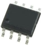
| 供应商器件封装 | 8-SO |
| 其它名称 | 497-5361-5 |
| 其它有关文件 | http://www.st.com/web/catalog/sense_power/FM142/CL1428/SC334/PF75482?referrer=70071840 |
| 包装 | 管件 |
| 商标 | STMicroelectronics |
| 安装类型 | 表面贴装 |
| 安装风格 | SMD/SMT |
| 封装 | Tube |
| 封装/外壳 | 8-SOIC(0.154",3.90mm 宽) |
| 封装/箱体 | SO-8 |
| 工作温度 | -40°C ~ 125°C |
| 工厂包装数量 | 1000 |
| 延迟时间 | - |
| 最大工作温度 | + 125 C |
| 最小工作温度 | - 40 C |
| 标准包装 | 100 |
| 激励器数量 | 2 Driver |
| 电压-电源 | 10 V ~ 16.6 V |
| 电流-峰值 | 175mA |
| 电源电压-最小 | 10 V |
| 电源电流 | 25 mA |
| 类型 | High Voltage Half Bridge |
| 系列 | L6571 |
| 输入类型 | 自振荡 |
| 输出数 | 2 |
| 输出端数量 | 2 |
| 配置 | Self-Oscillating |
| 配置数 | 1 |
| 高压侧电压-最大值(自举) | 600V |


- 商务部:美国ITC正式对集成电路等产品启动337调查
- 曝三星4nm工艺存在良率问题 高通将骁龙8 Gen1或转产台积电
- 太阳诱电将投资9.5亿元在常州建新厂生产MLCC 预计2023年完工
- 英特尔发布欧洲新工厂建设计划 深化IDM 2.0 战略
- 台积电先进制程称霸业界 有大客户加持明年业绩稳了
- 达到5530亿美元!SIA预计今年全球半导体销售额将创下新高
- 英特尔拟将自动驾驶子公司Mobileye上市 估值或超500亿美元
- 三星加码芯片和SET,合并消费电子和移动部门,撤换高东真等 CEO
- 三星电子宣布重大人事变动 还合并消费电子和移动部门
- 海关总署:前11个月进口集成电路产品价值2.52万亿元 增长14.8%


PDF Datasheet 数据手册内容提取
L6571 High voltage half bridge driver with oscillator Features ■ High voltage rail up to 600 V ■ BCD off line technology ■ 15.6 V Zener clamp on Vs ■ Driver current capability: DIP-8 SO8 – Sink current = 270 mA can be programmed using external resistor and – Source current = 170 mA capacitor. ■ Very low start up current: 150 mA The internal circuitry of the device allows it to be ■ Undervoltage lockout with hysteresis driven also by external logic signal. ■ Programmable oscillator frequency The output drivers are designed to drive external ■ Dead time 1.25 μs (L6571A) or 0.72 μs nchannel power MOSFET and IGBT. The internal (L6571B) logic assures a dead time to avoid cross- ■ dV/dt immunity up to ±50 V/ns conduction of the power devices. ■ ESD protection Two version are available: L6571A and L6571B. They differ in the internal dead time: 1.25μs and Description 0.72 μs (typ.) The device is a high voltage half bridge driver with built in oscillator. The frequency of the oscillator Figure 1. Block diagram (cid:43)(cid:17)(cid:57)(cid:17) (cid:38)(cid:57)(cid:54) (cid:53)(cid:43)(cid:57) (cid:57)(cid:54) (cid:37)(cid:50)(cid:50)(cid:55) (cid:20) (cid:27) (cid:37)(cid:44)(cid:36)(cid:54) (cid:47)(cid:40)(cid:57)(cid:40)(cid:47) (cid:26) (cid:43)(cid:57)(cid:42) (cid:38)(cid:37)(cid:50)(cid:50)(cid:55) (cid:53)(cid:40)(cid:42)(cid:56)(cid:47)(cid:36)(cid:55)(cid:50)(cid:53) (cid:54)(cid:43)(cid:44)(cid:41)(cid:55)(cid:40)(cid:53) (cid:43)(cid:44)(cid:42)(cid:43) (cid:54)(cid:44)(cid:39)(cid:40) (cid:57)(cid:54) (cid:39)(cid:53)(cid:44)(cid:57)(cid:40)(cid:53) (cid:53)(cid:41) (cid:21) (cid:37)(cid:56)(cid:41)(cid:41)(cid:40)(cid:53) (cid:25) (cid:50)(cid:56)(cid:55) (cid:47)(cid:50)(cid:36)(cid:39) (cid:53)(cid:41) (cid:38)(cid:41) (cid:22) (cid:38)(cid:50)(cid:48)(cid:51) (cid:57)(cid:54) (cid:38)(cid:41) (cid:47)(cid:50)(cid:58)(cid:3)(cid:54)(cid:44)(cid:39)(cid:40) (cid:39)(cid:53)(cid:44)(cid:57)(cid:40)(cid:53) (cid:38)(cid:50)(cid:48)(cid:51) (cid:47)(cid:50)(cid:42)(cid:44)(cid:38) (cid:47)(cid:57)(cid:42) (cid:42)(cid:49)(cid:39) (cid:23) (cid:24) (cid:39)(cid:28)(cid:25)(cid:44)(cid:49)(cid:23)(cid:22)(cid:22) January 2010 Doc ID 4946 Rev 6 1/12 www.st.com 12
Contents L6571A - L6571B Contents 1 Maximum ratings . . . . . . . . . . . . . . . . . . . . . . . . . . . . . . . . . . . . . . . . . . . . 3 1.1 Absolute maximum ratings . . . . . . . . . . . . . . . . . . . . . . . . . . . . . . . . . . . . . 3 1.2 Thermal data . . . . . . . . . . . . . . . . . . . . . . . . . . . . . . . . . . . . . . . . . . . . . . . 3 1.3 Recommended operating conditions . . . . . . . . . . . . . . . . . . . . . . . . . . . . . 3 2 Pin connection . . . . . . . . . . . . . . . . . . . . . . . . . . . . . . . . . . . . . . . . . . . . . . 4 3 Electrical data . . . . . . . . . . . . . . . . . . . . . . . . . . . . . . . . . . . . . . . . . . . . . . 5 4 Oscillator frequency . . . . . . . . . . . . . . . . . . . . . . . . . . . . . . . . . . . . . . . . . 6 5 Package mechanical data . . . . . . . . . . . . . . . . . . . . . . . . . . . . . . . . . . . . . 8 6 Order information . . . . . . . . . . . . . . . . . . . . . . . . . . . . . . . . . . . . . . . . . . 10 7 Revision history . . . . . . . . . . . . . . . . . . . . . . . . . . . . . . . . . . . . . . . . . . . 11 2/12 Doc ID 4946 Rev 6
L6571A - L6571B Maximum ratings 1 Maximum ratings 1.1 Absolute maximum ratings T able 1. Absolute maximum ratings Symbol Parameter Value Unit I (1) Supply current 25 mA S V Oscillator resistor voltage 18 V CF V Low side switch gate output 14.6 V LVG V High side switch source output -1 to V -18 V OUT BOOT V High side switch gate output -1 to V V HVG BOOT V Floating supply voltage 618 V BOOT V Floating supply vs OUT voltage 18 V BOOT/OUT dV VBOOT slew rate (Repetitive) ± 50 V/ns BOOT/dt dV VOUT slew rate (Repetitive) ± 50 V/ns OUT/dt T Storage temperature -40 to 150 °C stg T Junction temperature -40 to 150 °C J T Ambient temperature (Operative) -40 to 125 °C amb 1. The device has an internal zener clamp between GND and VS (typical 15.6 V).Therefore the circuit should not be driven by a DC low impedance power source. Note: ESD immunity for pins 6, 7 and 8 is guaranteed up to 900 V (human body model) 1.2 Thermal data T able 2. Thermal data Symbol Parameter MDIP8 SO8 Unit R Thermal resistance junction-ambient max 100 150 °C/W thJA 1.3 Recommended operating conditions T able 3. Recommended operating conditions Symbol Parameter Min. Max. Unit V Supply voltage 10 VCL V S V Floating supply voltage - 500 V BOOT VBOOT V High side switch source output -1 V OUT -VCL f Oscillation frequency 200 kHz out Doc ID 4946 Rev 6 3/12
Pin connection L6571A - L6571B 2 Pin connection Figure 2. Pin connection (cid:57) (cid:20) (cid:27) (cid:37)(cid:50)(cid:50)(cid:55) (cid:54) (cid:53)(cid:41) (cid:21) (cid:26) (cid:43)(cid:57)(cid:42) (cid:38) (cid:22) (cid:25) (cid:50)(cid:56)(cid:55) (cid:41) (cid:42)(cid:49)(cid:39) (cid:23) (cid:24) (cid:47)(cid:57)(cid:42) (cid:39)(cid:28)(cid:23)(cid:44)(cid:49)(cid:19)(cid:24)(cid:28) Table 4. Pin description N° Pin Description 1 VS Supply input voltage with internal clamp [typ. 15.6V] Oscillator timing resistor pin. A buffer set alternatively to VS and GND can provide current to the external resistor RF connected between pin 2 and 3. Alternatively, 2 RF the signal on pin 2 can be used also to drive another IC (i.e. another L6569/71 to drive a full H-bridge) Oscillator timing capacitor pin. A capacitor connected between this pin and GND 3 CF fixes (together with RF) the oscillating frequency Alternatively an external logic signal can be applied to the pin to drive the IC. 4 GND Ground Low side driver output. The output stage can deliver 170mA source and 270mA 5 LVG sink [typ.values]. 6 OUT Upper driver floating reference High side driver output. The output stage can deliver 170mA source and 270mA 7 HVG sink [typ.values]. 8 BOOT Bootstrap voltage supply. It is the upper driver floating supply. 4/12 Doc ID 4946 Rev 6
L6571A - L6571B Electrical data 3 Electrical data V = 12V; V - V = 12V; T = 25 °C; unless otherwise specified. S BOOT OUT j Table 5. Electrical characteristcs Symbol Pin Parameter Test Condition Min. Typ. Max. Unit V 1 VS turn on threshold 8.3 9 9.7 V SUVP V VS turn off threshold 7.3 8 8.7 V SUVN V VS hysteresis 0.7 1 1.3 V SUVH V VS clamping voltage I = 5 mA 14.6 15.6 16.6 V CL S I Start up current V < V 150 250 μA SU S SUVN I Quiescent current V > V 500 700 μA q S SUVP I 8 Leakage current BOOT pin vs GND V = 580V 5 μA BOOTLK BOOT I 6 Leakage current OUT pin vs GND V = 562V 5 μA OUTLK OUT I 7 High side driver source current V = 6V 110 175 mA HVG SO HVG I High side driver sink current V = 6V 190 275 mA HVG SI HVG I 5 Low side driver source current V = 6V 110 175 mA LVG SO LVG I Low side driver sink current V = 6V 190 275 mA LVG SI LVG V 2 RF high level output voltage I =1mA V -0.05 V -0.2 V RFON RF S S V RF low level output voltage I = -1mA 50 200 mV RF OFF RF V 3 CF upper threshold 7.7 8 8.2 V CFU V CF lower threshold 3.80 4 4.3 V CFL L6571A 0.85 1.25 1.65 μs t Internal dead time d L6571B 0.50 0.72 0.94 μs Duty cycle, ratio between dead DC Time + conduction time of high 0.45 0.5 0.55 Side and low side drivers I 1 Average current from Vs No Load, fs = 60KHz 1.2 1.5 mA AVE f 6 Oscillation frequency RT = 12K; CT = 1nF 57 60 63 kHz out Doc ID 4946 Rev 6 5/12
Oscillator frequency L6571A - L6571B 4 Oscillator frequency The frequency of the internal oscillator can be programmed using external resistor and capacitor. The nominal oscillator frequency can be calculated using the following equation: Equation 1 Where R and C are the external resistor and capacitor. F F The device can be driven in "shut down" condition keeping the C pin close to GND, but F some cares have to be taken: 1. When CF is to GND the high side driver is off and the low side is on 2. The forced discharge of the oscillator capacitor C must not be shorter than 1us: a F simple way to do this is to limit the current discharge with a resistive path imposing R · C > 1 μs (see fig.1) F Figure 3. Fault signal (cid:20) (cid:27) (cid:21) (cid:26) (cid:53) (cid:53)(cid:41) (cid:22) (cid:25) (cid:73)(cid:68)(cid:88)(cid:79)(cid:87)(cid:86)(cid:76)(cid:74)(cid:81)(cid:68)(cid:79) (cid:38)(cid:41) (cid:23) (cid:24) (cid:42)(cid:49)(cid:39)(cid:48) Figure 4. Waveforms (cid:57)(cid:54) (cid:57)(cid:54)(cid:56)(cid:57)(cid:51) (cid:57)(cid:38)(cid:41) (cid:47)(cid:57)(cid:42) (cid:55)(cid:20) (cid:39)(cid:28)(cid:25)(cid:44)(cid:49)(cid:23)(cid:22)(cid:23) (cid:55)(cid:38) 6/12 Doc ID 4946 Rev 6
L6571A - L6571B Oscillator frequency Figure 5. T ypical dead time vs. temperature Figure 6. Typical rise and fall times vs. load dependency (L6571A) capacitance (cid:39)(cid:72)(cid:68)(cid:71)(cid:3)(cid:87)(cid:76)(cid:80)(cid:72)(cid:3)(cid:62)(cid:77)(cid:86)(cid:72)(cid:70)(cid:64) (cid:87)(cid:76)(cid:80)(cid:72)(cid:3)(cid:62)(cid:81)(cid:86)(cid:72)(cid:70)(cid:64) (cid:20)(cid:17)(cid:26) (cid:39)(cid:28)(cid:25)(cid:44)(cid:49)(cid:22)(cid:26)(cid:27)(cid:36) (cid:22)(cid:19)(cid:19) (cid:39)(cid:28)(cid:25)(cid:44)(cid:49)(cid:23)(cid:20)(cid:26) (cid:20)(cid:17)(cid:25) (cid:21)(cid:24)(cid:19) (cid:55)(cid:85) (cid:20)(cid:17)(cid:24) (cid:21)(cid:19)(cid:19) (cid:20)(cid:17)(cid:23) (cid:20)(cid:24)(cid:19) (cid:20)(cid:17)(cid:22) (cid:55)(cid:73) (cid:20)(cid:17)(cid:21) (cid:20)(cid:19)(cid:19) (cid:20)(cid:17)(cid:20) (cid:24)(cid:19) (cid:20) (cid:19) (cid:19)(cid:17)(cid:28) (cid:19) (cid:20) (cid:21) (cid:22) (cid:23) (cid:24) (cid:25) (cid:16)(cid:24)(cid:19) (cid:19) (cid:24)(cid:19) (cid:20)(cid:19)(cid:19) (cid:20)(cid:24)(cid:19) (cid:38)(cid:3)(cid:62)(cid:81)(cid:41)(cid:64) (cid:55)(cid:72)(cid:80)(cid:83)(cid:72)(cid:85)(cid:68)(cid:87)(cid:88)(cid:85)(cid:72)(cid:3)(cid:62)(cid:38)(cid:64) (cid:41)(cid:82)(cid:85)(cid:3)(cid:69)(cid:82)(cid:87)(cid:75)(cid:3)(cid:75)(cid:76)(cid:74)(cid:75)(cid:3)(cid:68)(cid:81)(cid:71)(cid:3)(cid:79)(cid:82)(cid:90)(cid:3)(cid:86)(cid:76)(cid:71)(cid:72)(cid:3)(cid:69)(cid:88)(cid:73)(cid:73)(cid:72)(cid:85)(cid:86)(cid:3)(cid:35)(cid:21)(cid:24)(cid:219)(cid:38)(cid:3)(cid:55)(cid:68)(cid:80)(cid:69) Figure 7. Typical frequency vs temperature Figure 8. Quiescent current vs. supply dependency voltage (cid:41)(cid:85)(cid:72)(cid:84)(cid:88)(cid:72)(cid:81)(cid:70)(cid:92)(cid:3)(cid:62)(cid:46)(cid:43)(cid:93)(cid:64) (cid:25)(cid:24) (cid:39)(cid:28)(cid:25)(cid:44)(cid:49)(cid:22)(cid:26)(cid:28)(cid:36) (cid:44)(cid:84)(cid:3)(cid:11)(cid:77)(cid:36)(cid:12) (cid:39)(cid:28)(cid:25)(cid:44)(cid:49)(cid:23)(cid:20)(cid:27) (cid:25)(cid:23) (cid:20)(cid:19)(cid:23) (cid:25)(cid:22) (cid:25)(cid:21) (cid:25)(cid:20) (cid:20)(cid:19)(cid:22) (cid:25)(cid:19) (cid:24)(cid:28) (cid:20)(cid:19)(cid:21) (cid:24)(cid:27) (cid:24)(cid:26) (cid:24)(cid:25) (cid:20)(cid:19) (cid:24)(cid:24) (cid:16)(cid:24)(cid:19) (cid:16)(cid:21)(cid:24) (cid:19) (cid:21)(cid:24) (cid:24)(cid:19) (cid:26)(cid:24) (cid:20)(cid:19)(cid:19) (cid:20)(cid:21)(cid:24) (cid:55)(cid:72)(cid:80)(cid:83)(cid:72)(cid:85)(cid:68)(cid:87)(cid:88)(cid:85)(cid:72)(cid:62)(cid:38)(cid:64) (cid:19) (cid:21) (cid:23) (cid:25) (cid:27) (cid:20)(cid:19) (cid:20)(cid:21) (cid:20)(cid:23) (cid:57)(cid:54)(cid:11)(cid:57)(cid:12) Figure 9. Typical and theoretical oscillator frequency vs resistor value (cid:73)(cid:3)(cid:11)(cid:46)(cid:43)(cid:93)(cid:12) (cid:20)(cid:24)(cid:19) (cid:39)(cid:28)(cid:25)(cid:44)(cid:49)(cid:22)(cid:27)(cid:19) (cid:55)(cid:75)(cid:72)(cid:82)(cid:85)(cid:72)(cid:87)(cid:76)(cid:70)(cid:68)(cid:79) (cid:20)(cid:19)(cid:19) (cid:28)(cid:19) (cid:38)(cid:32)(cid:22)(cid:22)(cid:19)(cid:83)(cid:41) (cid:27)(cid:19) (cid:38)(cid:32)(cid:24)(cid:25)(cid:19)(cid:83)(cid:41) (cid:26)(cid:19) (cid:38)(cid:32)(cid:20)(cid:81)(cid:41) (cid:25)(cid:19) (cid:24)(cid:19) (cid:22)(cid:19) (cid:21)(cid:19) (cid:24) (cid:25) (cid:26) (cid:27) (cid:28)(cid:20)(cid:19) (cid:20)(cid:24) (cid:21)(cid:19) (cid:22)(cid:19) (cid:23)(cid:19) (cid:24)(cid:19) (cid:53)(cid:72)(cid:86)(cid:76)(cid:86)(cid:87)(cid:82)(cid:85)(cid:3)(cid:57)(cid:68)(cid:79)(cid:88)(cid:72)(cid:3)(cid:11)(cid:46)(cid:82)(cid:75)(cid:80)(cid:12) Doc ID 4946 Rev 6 7/12
Package mechanical data L6571A - L6571B 5 Package mechanical data In order to meet environmental requirements, ST offers these devices in different grades of ECOPACK® packages, depending on their level of environmental compliance. ECOPACK® specifications, grade definitions and product status are available at: www.st.com. ECOPACK® is an ST trademark. Figure 10. DIP-8 mechanical data mm inch DIM. OUTLINEAND MIN. TYP. MAX. MIN. TYP. MAX. MECHANICALDATA A 3.32 0.131 a1 0.51 0.020 B 1.15 1.65 0.045 0.065 b 0.356 0.55 0.014 0.022 b1 0.204 0.304 0.008 0.012 D 10.92 0.430 E 7.95 9.75 0.313 0.384 e 2.54 0.100 e3 7.62 0.300 e4 7.62 0.300 F 6.6 0.260 I 5.08 0.200 L 3.18 3.81 0.125 0.150 DIP-8 Z 1.52 0.060 8/12 Doc ID 4946 Rev 6
L6571A - L6571B Package mechanical data T able 1. SO-8 mechanical data mm. inch Dim. Min Typ Max Min Typ Max A 1.35 1.75 0.053 0.069 A1 0.10 0.25 0.004 0.010 A2 1.10 1.65 0.043 0.065 B 0.33 0.51 0.013 0.020 C 0.19 0.25 0.007 0.010 (1) 4.80 5.00 0.189 0.197 D E 3.80 4.00 0.15 0.157 e 1.27 0.050 H 5.80 6.20 0.228 0.244 h 0.25 0.50 0.010 0.020 L 0.40 1.27 0.016 0.050 k 0° (min.), 8° (max.) ddd 0.10 0.004 1. Dimensions D does not include mold flash, protru-sions or gate burrs. Mold flash, potrusions or gate burrs shall not exceed 0.15mm (.006inch) in total (both side). Figure 11. Package dimensions Doc ID 4946 Rev 6 9/12
Order information L6571A - L6571B 6 Order information Table 6. Ordering information Order codes Package Packaging L6571A DIP-8 Tube L6571AD SO8 L6571AD013TR Tape and reel L6571B DIP-8 Tube L6571BD SO8 L6571BD013TR Tape and reel 10/12 Doc ID 4946 Rev 6
L6571A - L6571B Revision history 7 Revision history Table 7. Document revision history Date Revision Changes 14-Jan-2004 5 No history because migration 15-Jan-2010 6 Updated Table6 on page10 Doc ID 4946 Rev 6 11/12
L6571A - L6571B Please Read Carefully: Information in this document is provided solely in connection with ST products. STMicroelectronics NV and its subsidiaries (“ST”) reserve the right to make changes, corrections, modifications or improvements, to this document, and the products and services described herein at any time, without notice. All ST products are sold pursuant to ST’s terms and conditions of sale. Purchasers are solely responsible for the choice, selection and use of the ST products and services described herein, and ST assumes no liability whatsoever relating to the choice, selection or use of the ST products and services described herein. No license, express or implied, by estoppel or otherwise, to any intellectual property rights is granted under this document. If any part of this document refers to any third party products or services it shall not be deemed a license grant by ST for the use of such third party products or services, or any intellectual property contained therein or considered as a warranty covering the use in any manner whatsoever of such third party products or services or any intellectual property contained therein. UNLESS OTHERWISE SET FORTH IN ST’S TERMS AND CONDITIONS OF SALE ST DISCLAIMS ANY EXPRESS OR IMPLIED WARRANTY WITH RESPECT TO THE USE AND/OR SALE OF ST PRODUCTS INCLUDING WITHOUT LIMITATION IMPLIED WARRANTIES OF MERCHANTABILITY, FITNESS FOR A PARTICULAR PURPOSE (AND THEIR EQUIVALENTS UNDER THE LAWS OF ANY JURISDICTION), OR INFRINGEMENT OF ANY PATENT, COPYRIGHT OR OTHER INTELLECTUAL PROPERTY RIGHT. UNLESS EXPRESSLY APPROVED IN WRITING BY AN AUTHORIZED ST REPRESENTATIVE, ST PRODUCTS ARE NOT RECOMMENDED, AUTHORIZED OR WARRANTED FOR USE IN MILITARY, AIR CRAFT, SPACE, LIFE SAVING, OR LIFE SUSTAINING APPLICATIONS, NOR IN PRODUCTS OR SYSTEMS WHERE FAILURE OR MALFUNCTION MAY RESULT IN PERSONAL INJURY, DEATH, OR SEVERE PROPERTY OR ENVIRONMENTAL DAMAGE. ST PRODUCTS WHICH ARE NOT SPECIFIED AS "AUTOMOTIVE GRADE" MAY ONLY BE USED IN AUTOMOTIVE APPLICATIONS AT USER’S OWN RISK. Resale of ST products with provisions different from the statements and/or technical features set forth in this document shall immediately void any warranty granted by ST for the ST product or service described herein and shall not create or extend in any manner whatsoever, any liability of ST. ST and the ST logo are trademarks or registered trademarks of ST in various countries. Information in this document supersedes and replaces all information previously supplied. The ST logo is a registered trademark of STMicroelectronics. All other names are the property of their respective owners. © 2010 STMicroelectronics - All rights reserved STMicroelectronics group of companies Australia - Belgium - Brazil - Canada - China - Czech Republic - Finland - France - Germany - Hong Kong - India - Israel - Italy - Japan - Malaysia - Malta - Morocco - Philippines - Singapore - Spain - Sweden - Switzerland - United Kingdom - United States of America www.st.com 12/12 Doc ID 4946 Rev 6