ICGOO在线商城 > 分立半导体产品 > 二极管 - 整流器 - 阵列 > PMEG4005CT,215
 Datasheet下载
- 型号: PMEG4005CT,215
- 制造商: NXP Semiconductors
- 库位|库存: xxxx|xxxx
- 要求:
| 数量阶梯 | 香港交货 | 国内含税 |
| +xxxx | $xxxx | ¥xxxx |
查看当月历史价格
查看今年历史价格
PMEG4005CT,215产品简介:
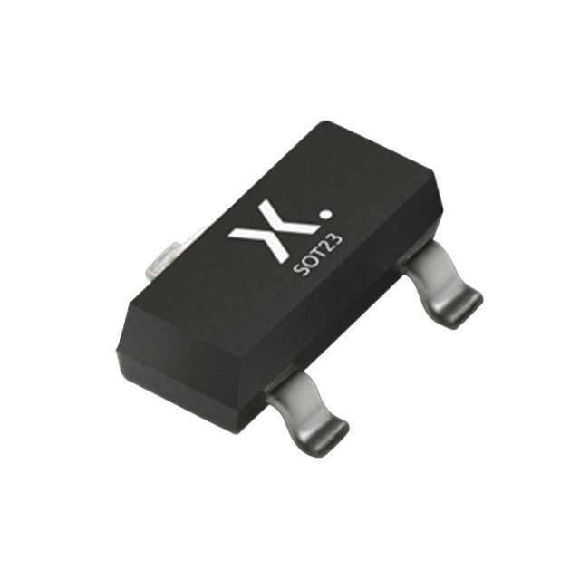
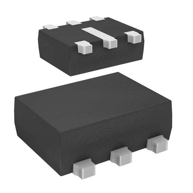
ICGOO电子元器件商城为您提供PMEG4005CT,215由NXP Semiconductors设计生产,在icgoo商城现货销售,并且可以通过原厂、代理商等渠道进行代购。 PMEG4005CT,215价格参考¥0.94-¥0.94。NXP SemiconductorsPMEG4005CT,215封装/规格:二极管 - 整流器 - 阵列, Diode Array 1 Pair Common Cathode Schottky 40V 500mA Surface Mount TO-236-3, SC-59, SOT-23-3。您可以下载PMEG4005CT,215参考资料、Datasheet数据手册功能说明书,资料中有PMEG4005CT,215 详细功能的应用电路图电压和使用方法及教程。
Nexperia USA Inc. 的 PMEG4005CT,215 是一款表面贴装肖特基势垒二极管阵列,属于二极管-整流器-阵列类别。该器件采用SOT23封装,内部集成了两个独立的肖特基二极管,具有低正向压降(典型值0.48V)和快速开关特性,适用于高效率、低功耗的应用场景。

PMEG4005CT,215广泛应用于便携式电子设备和消费类电子产品中,如智能手机、平板电脑、可穿戴设备和无线耳机等,常用于电源管理电路中的反向电压保护、电池充放电路径隔离、以及防止外部电源反接损坏系统。此外,其低漏电流和高可靠性也使其适合用于USB接口的电源保护、DC-DC转换器输出整流、以及信号引脚的静电和过压防护。

在工业控制和通信设备中,该器件可用于为敏感电路提供瞬态电压抑制和极性保护。由于其小型化SOT23封装,非常适合空间受限的高密度PCB布局,有助于实现产品的小型化和轻薄化设计。

总之,PMEG4005CT,215凭借其高效能、小尺寸和高可靠性,主要应用于对空间和能效要求较高的消费电子、移动设备和电源管理领域,是现代电子系统中理想的保护与整流元件。
| 参数 | 数值 |
| 产品目录 | |
| 描述 | DIODE SCHOTTKY 40V 500MA TO236AB肖特基二极管与整流器 SCHOTTKY DIODE 31ACDBZR/SOT |
| 产品分类 | 二极管,整流器 - 阵列分离式半导体 |
| 品牌 | NXP Semiconductors |
| 产品手册 | |
| 产品图片 |
|
| rohs | 符合RoHS无铅 / 符合限制有害物质指令(RoHS)规范要求 |
| 产品系列 | 二极管与整流器,肖特基二极管与整流器,NXP Semiconductors PMEG4005CT,215- |
| 数据手册 | |
| 产品型号 | PMEG4005CT,215 |
| PCN封装 | |
| PCN设计/规格 | |
| 不同If时的电压-正向(Vf) | 470mV @ 500mA |
| 不同 Vr时的电流-反向漏电流 | 100µA @ 40V |
| 二极管类型 | |
| 二极管配置 | 1 对共阴极 |
| 产品 | Schottky Rectifiers |
| 产品种类 | 肖特基二极管与整流器 |
| 供应商器件封装 | SOT-23 (TO-236AB) |
| 其它名称 | 568-6522-2 |
| 包装 | 带卷 (TR) |
| 反向恢复时间(trr) | 13ns |
| 商标 | NXP Semiconductors |
| 安装类型 | 表面贴装 |
| 安装风格 | SMD/SMT |
| 封装 | Reel |
| 封装/外壳 | TO-236-3,SC-59,SOT-23-3 |
| 封装/箱体 | SOT-23 |
| 峰值反向电压 | 40 V |
| 工作温度范围 | + 150 C |
| 工厂包装数量 | 3000 |
| 技术 | Silicon |
| 最大功率耗散 | 330 mW |
| 最大反向漏泄电流 | 100 uA |
| 最大工作温度 | + 150 C |
| 最大浪涌电流 | 10 A |
| 最小工作温度 | - 55 C |
| 标准包装 | 3,000 |
| 正向电压下降 | 410 mV |
| 正向连续电流 | 0.5 A |
| 热阻 | 60°C/W Jl |
| 电压-DC反向(Vr)(最大值) | 40V |
| 电流-平均整流(Io)(每二极管) | 500mA |
| 速度 | 快速恢复 =< 500 ns,> 200mA(Io) |
| 配置 | Dual Common Cathode |


- 商务部:美国ITC正式对集成电路等产品启动337调查
- 曝三星4nm工艺存在良率问题 高通将骁龙8 Gen1或转产台积电
- 太阳诱电将投资9.5亿元在常州建新厂生产MLCC 预计2023年完工
- 英特尔发布欧洲新工厂建设计划 深化IDM 2.0 战略
- 台积电先进制程称霸业界 有大客户加持明年业绩稳了
- 达到5530亿美元!SIA预计今年全球半导体销售额将创下新高
- 英特尔拟将自动驾驶子公司Mobileye上市 估值或超500亿美元
- 三星加码芯片和SET,合并消费电子和移动部门,撤换高东真等 CEO
- 三星电子宣布重大人事变动 还合并消费电子和移动部门
- 海关总署:前11个月进口集成电路产品价值2.52万亿元 增长14.8%


PDF Datasheet 数据手册内容提取
Important notice Dear Customer, On 7 February 2017 the former NXP Standard Product business became a new company with the tradename Nexperia. Nexperia is an industry leading supplier of Discrete, Logic and PowerMOS semiconductors with its focus on the automotive, industrial, computing, consumer and wearable application markets In data sheets and application notes which still contain NXP or Philips Semiconductors references, use the references to Nexperia, as shown below. Instead of http://www.nxp.com, http://www.philips.com/ or http://www.semiconductors.philips.com/, use http://www.nexperia.com Instead of sales.addresses@www.nxp.com or sales.addresses@www.semiconductors.philips.com, use salesaddresses@nexperia.com (email) Replace the copyright notice at the bottom of each page or elsewhere in the document, depending on the version, as shown below: - © NXP N.V. (year). All rights reserved or © Koninklijke Philips Electronics N.V. (year). All rights reserved Should be replaced with: - © Nexperia B.V. (year). All rights reserved. If you have any questions related to the data sheet, please contact our nearest sales office via e-mail or telephone (details via salesaddresses@nexperia.com). Thank you for your cooperation and understanding, Kind regards, Team Nexperia
PMEG4005CT 500 mA low V dual MEGA Schottky barrier rectifier F Rev. 2 — 20 September 2010 Product data sheet 1. Product profile 1.1 General description Planar Maximum Efficiency General Application(MEGA) Schottky barrier rectifier in common cathode configuration with an integrated guard ring for stress protection, encapsulated in a SOT23(TO-236AB) small Surface-Mounted Device(SMD) plastic package. 1.2 Features and benefits (cid:132) Average forward current: I ≤0.5A (cid:132) AEC-Q101 qualified F(AV) (cid:132) Reverse voltage: V ≤40V (cid:132) Small SMD plastic package R (cid:132) Low forward voltage 1.3 Applications (cid:132) Low voltage rectification (cid:132) Reverse polarity protection (cid:132) High efficiency DC-to-DC conversion (cid:132) High-speed switching (cid:132) Switch Mode Power Supply(SMPS) (cid:132) Low power consumption applications 1.4 Quick reference data Table 1. Quick reference data T =25°C unless otherwise specified. j Symbol Parameter Conditions Min Typ Max Unit Per diode I average forward current square wave; F(AV) δ=0.5; f=20kHz T ≤85°C [1] - - 0.5 A amb T ≤130°C - - 0.5 A sp V reverse voltage - - 40 V R V forward voltage I =0.5A - 410 470 mV F F I reverse current V =40V - 27 100 μA R R [1] Device mounted on a ceramicPrinted-Circuit Board(PCB), Al O , standard footprint. 2 3
PMEG4005CT NXP Semiconductors 500 mA low V dual MEGA Schottky barrier rectifier F 2. Pinning information Table 2. Pinning Pin Description Simplified outline Graphic symbol 1 anode(diode1) 3 3 2 anode(diode2) 3 commoncathode 1 2 1 2 006aaa438 3. Ordering information Table 3. Ordering information Type number Package Name Description Version PMEG4005CT - plastic surface-mounted package; 3leads SOT23 4. Marking Table 4. Marking codes Type number Marking code[1] PMEG4005CT PA* [1] * = -: made in Hong Kong * = p: made in Hong Kong * = t: made in Malaysia * = W: made in China 5. Limiting values Table 5. Limiting values In accordance with the Absolute Maximum Rating System (IEC 60134). Symbol Parameter Conditions Min Max Unit Per diode V reverse voltage T =25°C - 40 V R j I average forward current square wave; F(AV) δ=0.5; f=20kHz T ≤85°C [1] - 0.5 A amb T ≤130°C - 0.5 A sp I repetitive peak forward t ≤1ms; - 3.9 A FRM p current δ≤0.25 I non-repetitive peak square wave; [2] - 10 A FSM forward current t =8ms p PMEG4005CT All information provided in this document is subject to legal disclaimers. © NXP B.V. 2010. All rights reserved. Product data sheet Rev. 2 — 20 September 2010 2 of 14
PMEG4005CT NXP Semiconductors 500 mA low V dual MEGA Schottky barrier rectifier F Table 5. Limiting values …continued In accordance with the Absolute Maximum Rating System (IEC 60134). Symbol Parameter Conditions Min Max Unit Per device; one diode loaded P total power dissipation T ≤25°C [3] - 330 mW tot amb [4] - 400 mW [1] - 460 mW T junction temperature - 150 °C j T ambient temperature −55 +150 °C amb T storage temperature −65 +150 °C stg [1] Device mounted on a ceramicPCB, Al O , standard footprint. 2 3 [2] Tj=25°C prior to surge. [3] Device mounted on an FR4PCB, single-sided copper, tin-plated and standard footprint. [4] Device mounted on an FR4PCB, single-sided copper, tin-plated, mounting pad for cathode 1cm2. 6. Thermal characteristics Table 6. Thermal characteristics Symbol Parameter Conditions Min Typ Max Unit Per diode; one diode loaded R thermal resistance from in free air [1] th(j-a) junction to ambient [2] - - 375 K/W [3] - - 310 K/W [4] - - 270 K/W R thermal resistance from [5] - - 60 K/W th(j-sp) junction to solder point [1] For Schottky barrier diodes thermal runaway has to be considered, as in some applications the reverse power losses P are a significant part of the total power losses. R [2] Device mounted on an FR4PCB, single-sided copper, tin-plated and standard footprint. [3] Device mounted on an FR4PCB, single-sided copper, tin-plated, mounting pad for cathode 1cm2. [4] Device mounted on a ceramicPCB, Al O , standard footprint. 2 3 [5] Soldering point of cathode tab. PMEG4005CT All information provided in this document is subject to legal disclaimers. © NXP B.V. 2010. All rights reserved. Product data sheet Rev. 2 — 20 September 2010 3 of 14
PMEG4005CT NXP Semiconductors 500 mA low V dual MEGA Schottky barrier rectifier F 103 006aab533 duty cycle = Zth(j-a) 1 (K/W) 0.75 0.5 0.33 102 0.25 0.2 0.1 0.05 0.02 0.01 10 0 1 10−3 10−2 10−1 1 10 102 103 tp (s) FR4PCB, standard footprint Fig 1. Transient thermal impedance from junction to ambient as a function of pulse duration; typical values 103 006aab534 duty cycle = Zth(j-a) (K/W) 1 0.75 0.5 102 0.33 0.25 0.2 0.1 0.05 0.02 0.01 10 0 1 10−3 10−2 10−1 1 10 102 103 tp (s) FR4PCB, mounting pad for cathode 1cm2 Fig 2. Transient thermal impedance from junction to ambient as a function of pulse duration; typical values PMEG4005CT All information provided in this document is subject to legal disclaimers. © NXP B.V. 2010. All rights reserved. Product data sheet Rev. 2 — 20 September 2010 4 of 14
PMEG4005CT NXP Semiconductors 500 mA low V dual MEGA Schottky barrier rectifier F 103 006aab535 duty cycle = Zth(j-a) (K/W) 1 0.75 0.5 102 0.33 0.25 0.2 0.1 0.05 0.02 0.01 10 0 1 10−3 10−2 10−1 1 10 102 103 tp (s) CeramicPCB, Al O , standard footprint 2 3 Fig 3. Transient thermal impedance from junction to ambient as a function of pulse duration; typical values 7. Characteristics Table 7. Characteristics T =25°C unless otherwise specified. j Symbol Parameter Conditions Min Typ Max Unit Per diode V forward voltage I =0.1mA - 95 130 mV F F I =1mA - 155 210 mV F I =10mA - 220 270 mV F I =100mA - 295 350 mV F I =500mA - 410 470 mV F I reverse current V =10V - 7 20 μA R R V =40V - 27 100 μA R C diode capacitance V =1V; f=1MHz - 43 50 pF d R t reverse recovery time [1] - 13 - ns rr [1] When switched from IF=10mA to IR=10mA; RL=100Ω; measured at IR=1mA. PMEG4005CT All information provided in this document is subject to legal disclaimers. © NXP B.V. 2010. All rights reserved. Product data sheet Rev. 2 — 20 September 2010 5 of 14
PMEG4005CT NXP Semiconductors 500 mA low V dual MEGA Schottky barrier rectifier F 10 006aab554 10−2 006aab555 IF (IAR) (1) (A) 10−3 1 (2) (1) 10−4 (2) 10−1 10−5 (3) 10−2 (3) (4) (5) 10−6 10−7 10−3 10−8 (4) 10−4 10−9 0.0 0.1 0.2 0.3 0.4 0.5 0.6 0.7 0 10 20 30 40 VF (V) VR (V) (1) Tj=150°C (1) Tj=125°C (2) Tj=125°C (2) Tj=85°C (3) Tj=85°C (3) Tj=25°C (4) Tj=25°C (4) Tj=−40°C (5) Tj=−40°C Fig 4. Forward current as a function of forward Fig 5. Reverse current as a function of reverse voltage; typical values voltage; typical values 006aab556 100 Cd (pF) 80 60 40 20 0 0 10 20 30 40 VR (V) f=1MHz; Tamb=25°C Fig 6. Diode capacitance as a function of reverse voltage; typical values PMEG4005CT All information provided in this document is subject to legal disclaimers. © NXP B.V. 2010. All rights reserved. Product data sheet Rev. 2 — 20 September 2010 6 of 14
PMEG4005CT NXP Semiconductors 500 mA low V dual MEGA Schottky barrier rectifier F 006aab557 006aab558 0.4 0.25 PF(AV) PR(W(A)V) (W) (4) 0.20 0.3 (3) 0.15 (2) (1) 0.2 (2) (1) (3) 0.10 0.1 (4) 0.05 0.0 0.0 0.0 0.25 0.50 0.75 0 5 10 15 20 25 IF(AV) (A) VR (V) Tj=150°C Tj=125°C (1) δ=0.1 (1) δ=1 (2) δ=0.2 (2) δ=0.9 (3) δ=0.5 (3) δ=0.8 (4) δ=1 (4) δ=0.5 Fig 7. Average forward power dissipation as a Fig 8. Average reverse power dissipation as a function of average forward current; typical function of reverse voltage; typical values values 006aab559 006aab560 0.75 0.75 (1) (1) IF(AV) IF(AV) (A) (A) (2) (2) 0.50 0.50 (3) (3) 0.25 (4) 0.25 (4) 0.0 0.0 0 25 50 75 100 125 150 175 0 25 50 75 100 125 150 175 Tamb (°C) Tamb (°C) FR4PCB, standard footprint FR4PCB, mounting pad for cathode 1cm2 Tj=150°C Tj=150°C (1) δ=1; DC (1) δ=1; DC (2) δ=0.5; f=20kHz (2) δ=0.5; f=20kHz (3) δ=0.2; f=20kHz (3) δ=0.2; f=20kHz (4) δ=0.1; f=20kHz (4) δ=0.1; f=20kHz Fig 9. Average forward current as a function of Fig 10. Average forward current as a function of ambient temperature; typical values ambient temperature; typical values PMEG4005CT All information provided in this document is subject to legal disclaimers. © NXP B.V. 2010. All rights reserved. Product data sheet Rev. 2 — 20 September 2010 7 of 14
PMEG4005CT NXP Semiconductors 500 mA low V dual MEGA Schottky barrier rectifier F 006aab561 006aab562 0.75 0.75 (1) (1) IF(AV) IF(AV) (A) (A) (2) (2) 0.50 0.50 (3) (3) 0.25 (4) 0.25 (4) 0.0 0.0 0 25 50 75 100 125 150 175 0 25 50 75 100 125 150 175 Tamb (°C) Tsp (°C) CeramicPCB, Al2O3, standard footprint Tj=150°C Tj=150°C (1) δ=1; DC (1) δ=1; DC (2) δ=0.5; f=20kHz (2) δ=0.5; f=20kHz (3) δ=0.2; f=20kHz (3) δ=0.2; f=20kHz (4) δ=0.1; f=20kHz (4) δ=0.1; f=20kHz Fig 11. Average forward current as a function of Fig 12. Average forward current as a function of ambient temperature; typical values solder point temperature; typical values 8. Test information tr tp t D.U.T. 10 % RS = 50 Ω IF SAMPLING + IF trr t OSCILLOSCOPE V = VR + IF × RS Ri = 50 Ω 90 % (1) VR mga881 input signal output signal (1) I =1mA R Input signal: reverse pulse rise time tr=0.6ns; reverse voltage pulse duration tp=100ns; duty cycle δ=0.05 Oscilloscope: rise time t =0.35ns r Fig 13. Reverse recovery time test circuit and waveforms PMEG4005CT All information provided in this document is subject to legal disclaimers. © NXP B.V. 2010. All rights reserved. Product data sheet Rev. 2 — 20 September 2010 8 of 14
PMEG4005CT NXP Semiconductors 500 mA low V dual MEGA Schottky barrier rectifier F P duty cycle δ = t1 t2 t2 t1 t 006aaa812 Fig 14. Duty cycle definition The current ratings for the typical waveforms as shown in Figure9, 10, 11 and 12 are calculated according to the equations: I = I ×δ with I defined as peakcurrent, F(AV) M M I = I at DC, and I = I × δ with I defined as RMScurrent. RMS F(AV) RMS M RMS 8.1 Quality information This product has been qualified in accordance with the Automotive Electronics Council (AEC) standard Q101 - Stress test qualification for discrete semiconductors, and is suitable for use in automotive applications. 9. Package outline 3.0 1.1 2.8 0.9 3 0.45 0.15 2.5 1.4 2.1 1.2 1 2 0.48 0.15 0.38 0.09 1.9 Dimensions in mm 04-11-04 Fig 15. Package outline SOT23(TO-236AB) 10. Packing information Table 8. Packing methods The indicated -xxx are the last three digits of the 12NC ordering code.[1] Type number Package Description Packing quantity 3000 10000 PMEG4005CT SOT23 4mm pitch, 8mm tape and reel -215 -235 PMEG4005CT All information provided in this document is subject to legal disclaimers. © NXP B.V. 2010. All rights reserved. Product data sheet Rev. 2 — 20 September 2010 9 of 14
PMEG4005CT NXP Semiconductors 500 mA low V dual MEGA Schottky barrier rectifier F [1] For further information and the availability of packing methods, see Section14. 11. Soldering 3.3 2.9 1.9 solder lands solder resist 3 1.7 2 solder paste 0.7 0.6 occupied area (3×) (3×) Dimensions in mm 0.5 (3×) 0.6 (3×) 1 sot023_fr Fig 16. Reflow soldering footprint SOT23(TO-236AB) 2.2 1.2 (2×) 1.4 (2×) solder lands 4.6 2.6 solder resist occupied area Dimensions in mm 1.4 preferred transport direction during soldering 2.8 4.5 sot023_fw Fig 17. Wave soldering footprint SOT23(TO-236AB) PMEG4005CT All information provided in this document is subject to legal disclaimers. © NXP B.V. 2010. All rights reserved. Product data sheet Rev. 2 — 20 September 2010 10 of 14
PMEG4005CT NXP Semiconductors 500 mA low V dual MEGA Schottky barrier rectifier F 12. Revision history Table 9. Revision history Document ID Release date Data sheet status Change notice Supersedes PMEG4005CTv.2 20100920 Product data sheet - PMEG4005CT_1 Modifications: • Table 2 “Pinning”: Graphic symbol amended • Section 13 “Legal information”: updated PMEG4005CT_1 20090605 Product data sheet - - PMEG4005CT All information provided in this document is subject to legal disclaimers. © NXP B.V. 2010. All rights reserved. Product data sheet Rev. 2 — 20 September 2010 11 of 14
PMEG4005CT NXP Semiconductors 500 mA low V dual MEGA Schottky barrier rectifier F 13. Legal information 13.1 Data sheet status Document status[1][2] Product status[3] Definition Objective [short] data sheet Development This document contains data from the objective specification for product development. Preliminary [short] data sheet Qualification This document contains data from the preliminary specification. Product [short] data sheet Production This document contains the product specification. [1] Please consult the most recently issued document before initiating or completing a design. [2] The term ‘short data sheet’ is explained in section “Definitions”. [3] The product status of device(s) described in this document may have changed since this document was published and may differ in case of multiple devices. The latest product status information is available on the Internet at URLhttp://www.nxp.com. 13.2 Definitions malfunction of an NXP Semiconductors product can reasonably be expected to result in personal injury, death or severe property or environmental damage. NXP Semiconductors accepts no liability for inclusion and/or use of Draft — The document is a draft version only. The content is still under NXP Semiconductors products in such equipment or applications and internal review and subject to formal approval, which may result in therefore such inclusion and/or use is at the customer’s own risk. modifications or additions. NXP Semiconductors does not give any representations or warranties as to the accuracy or completeness of Applications — Applications that are described herein for any of these information included herein and shall have no liability for the consequences of products are for illustrative purposes only. NXP Semiconductors makes no use of such information. representation or warranty that such applications will be suitable for the specified use without further testing or modification. Short data sheet — A short data sheet is an extract from a full data sheet with the same product type number(s) and title. A short data sheet is intended Customers are responsible for the design and operation of their applications for quick reference only and should not be relied upon to contain detailed and and products using NXP Semiconductors products, and NXP Semiconductors full information. For detailed and full information see the relevant full data accepts no liability for any assistance with applications or customer product sheet, which is available on request via the local NXP Semiconductors sales design. It is customer’s sole responsibility to determine whether the NXP office. In case of any inconsistency or conflict with the short data sheet, the Semiconductors product is suitable and fit for the customer’s applications and full data sheet shall prevail. products planned, as well as for the planned application and use of customer’s third party customer(s). Customers should provide appropriate Product specification — The information and data provided in a Product design and operating safeguards to minimize the risks associated with their data sheet shall define the specification of the product as agreed between applications and products. NXP Semiconductors and its customer, unless NXP Semiconductors and NXP Semiconductors does not accept any liability related to any default, customer have explicitly agreed otherwise in writing. In no event however, damage, costs or problem which is based on any weakness or default in the shall an agreement be valid in which the NXP Semiconductors product is customer’s applications or products, or the application or use by customer’s deemed to offer functions and qualities beyond those described in the third party customer(s). Customer is responsible for doing all necessary Product data sheet. testing for the customer’s applications and products using NXP Semiconductors products in order to avoid a default of the applications and 13.3 Disclaimers the products or of the application or use by customer’s third party customer(s). NXP does not accept any liability in this respect. Limited warranty and liability — Information in this document is believed to Limiting values — Stress above one or more limiting values (as defined in be accurate and reliable. However, NXP Semiconductors does not give any the Absolute Maximum Ratings System of IEC60134) will cause permanent representations or warranties, expressed or implied, as to the accuracy or damage to the device. Limiting values are stress ratings only and (proper) completeness of such information and shall have no liability for the operation of the device at these or any other conditions above those given in consequences of use of such information. the Recommended operating conditions section (if present) or the Characteristics sections of this document is not warranted. Constant or In no event shall NXP Semiconductors be liable for any indirect, incidental, repeated exposure to limiting values will permanently and irreversibly affect punitive, special or consequential damages (including - without limitation - lost the quality and reliability of the device. profits, lost savings, business interruption, costs related to the removal or replacement of any products or rework charges) whether or not such Terms and conditions of commercial sale — NXP Semiconductors damages are based on tort (including negligence), warranty, breach of products are sold subject to the general terms and conditions of commercial contract or any other legal theory. sale, as published at http://www.nxp.com/profile/terms, unless otherwise Notwithstanding any damages that customer might incur for any reason agreed in a valid written individual agreement. In case an individual whatsoever, NXP Semiconductors’ aggregate and cumulative liability towards agreement is concluded only the terms and conditions of the respective customer for the products described herein shall be limited in accordance agreement shall apply. NXP Semiconductors hereby expressly objects to with the Terms and conditions of commercial sale of NXP Semiconductors. applying the customer’s general terms and conditions with regard to the purchase of NXP Semiconductors products by customer. Right to make changes — NXP Semiconductors reserves the right to make changes to information published in this document, including without No offer to sell or license — Nothing in this document may be interpreted or limitation specifications and product descriptions, at any time and without construed as an offer to sell products that is open for acceptance or the grant, notice. This document supersedes and replaces all information supplied prior conveyance or implication of any license under any copyrights, patents or to the publication hereof. other industrial or intellectual property rights. Suitability for use — NXP Semiconductors products are not designed, Export control — This document as well as the item(s) described herein authorized or warranted to be suitable for use in life support, life-critical or may be subject to export control regulations. Export might require a prior safety-critical systems or equipment, nor in applications where failure or authorization from national authorities. PMEG4005CT All information provided in this document is subject to legal disclaimers. © NXP B.V. 2010. All rights reserved. Product data sheet Rev. 2 — 20 September 2010 12 of 14
PMEG4005CT NXP Semiconductors 500 mA low V dual MEGA Schottky barrier rectifier F Quick reference data — The Quick reference data is an extract of the 13.4 Trademarks product data given in the Limiting values and Characteristics sections of this document, and as such is not complete, exhaustive or legally binding. Notice: All referenced brands, product names, service names and trademarks are the property of their respective owners. 14. Contact information For more information, please visit: http://www.nxp.com For sales office addresses, please send an email to: salesaddresses@nxp.com PMEG4005CT All information provided in this document is subject to legal disclaimers. © NXP B.V. 2010. All rights reserved. Product data sheet Rev. 2 — 20 September 2010 13 of 14
PMEG4005CT NXP Semiconductors 500 mA low V dual MEGA Schottky barrier rectifier F 15. Contents 1 Product profile. . . . . . . . . . . . . . . . . . . . . . . . . . 1 1.1 General description . . . . . . . . . . . . . . . . . . . . . 1 1.2 Features and benefits. . . . . . . . . . . . . . . . . . . . 1 1.3 Applications . . . . . . . . . . . . . . . . . . . . . . . . . . . 1 1.4 Quick reference data . . . . . . . . . . . . . . . . . . . . 1 2 Pinning information. . . . . . . . . . . . . . . . . . . . . . 2 3 Ordering information. . . . . . . . . . . . . . . . . . . . . 2 4 Marking. . . . . . . . . . . . . . . . . . . . . . . . . . . . . . . . 2 5 Limiting values. . . . . . . . . . . . . . . . . . . . . . . . . . 2 6 Thermal characteristics . . . . . . . . . . . . . . . . . . 3 7 Characteristics. . . . . . . . . . . . . . . . . . . . . . . . . . 5 8 Test information. . . . . . . . . . . . . . . . . . . . . . . . . 8 8.1 Quality information . . . . . . . . . . . . . . . . . . . . . . 9 9 Package outline. . . . . . . . . . . . . . . . . . . . . . . . . 9 10 Packing information . . . . . . . . . . . . . . . . . . . . . 9 11 Soldering . . . . . . . . . . . . . . . . . . . . . . . . . . . . . 10 12 Revision history. . . . . . . . . . . . . . . . . . . . . . . . 11 13 Legal information. . . . . . . . . . . . . . . . . . . . . . . 12 13.1 Data sheet status . . . . . . . . . . . . . . . . . . . . . . 12 13.2 Definitions. . . . . . . . . . . . . . . . . . . . . . . . . . . . 12 13.3 Disclaimers. . . . . . . . . . . . . . . . . . . . . . . . . . . 12 13.4 Trademarks. . . . . . . . . . . . . . . . . . . . . . . . . . . 13 14 Contact information. . . . . . . . . . . . . . . . . . . . . 13 15 Contents. . . . . . . . . . . . . . . . . . . . . . . . . . . . . . 14 Please be aware that important notices concerning this document and the product(s) described herein, have been included in section ‘Legal information’. © NXP B.V. 2010. All rights reserved. For more information, please visit: http://www.nxp.com For sales office addresses, please send an email to: salesaddresses@nxp.com Date of release: 20 September 2010 Document identifier: PMEG4005CT