ICGOO在线商城 > 射频/IF 和 RFID > 衰减器 > PE43702MLI-Z
 Datasheet下载
- 型号: PE43702MLI-Z
- 制造商: Peregrine
- 库位|库存: xxxx|xxxx
- 要求:
| 数量阶梯 | 香港交货 | 国内含税 |
| +xxxx | $xxxx | ¥xxxx |
查看当月历史价格
查看今年历史价格
PE43702MLI-Z产品简介:
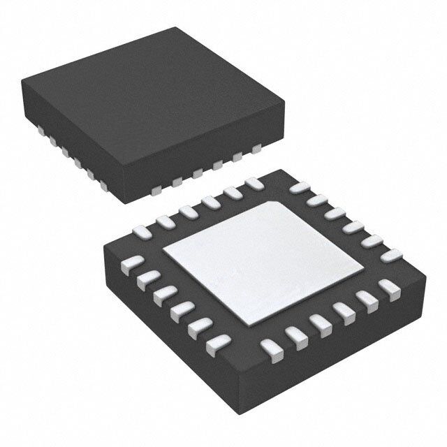
ICGOO电子元器件商城为您提供PE43702MLI-Z由Peregrine设计生产,在icgoo商城现货销售,并且可以通过原厂、代理商等渠道进行代购。 PE43702MLI-Z价格参考。PeregrinePE43702MLI-Z封装/规格:衰减器, RF Attenuator 31.75dB ±0.3dB 9kHz ~ 4GHz 50 Ohms 24-VFQFN Exposed Pad。您可以下载PE43702MLI-Z参考资料、Datasheet数据手册功能说明书,资料中有PE43702MLI-Z 详细功能的应用电路图电压和使用方法及教程。
pSemi(现为Qorvo旗下品牌)的PE43702MLI-Z是一款数字控制衰减器,广泛应用于需要精确射频信号调节的场景。该器件支持31 dB的衰减范围,步进为0.5 dB,工作频率覆盖10 MHz至8 GHz,适用于宽频带系统。其主要应用场景包括无线通信基础设施,如5G宏基站和小基站,用于实现自动增益控制和功率调节;在射频测试测量设备中,作为可编程衰减模块,提高测试精度与灵活性;此外,也适用于宽带固定无线接入、微波点对点通信和卫星通信终端,满足高频、高性能信号链需求。PE43702MLI-Z采用紧凑的6引脚MCM封装,具备低插入损耗和高线性度,适合对空间和性能要求较高的设计。整体上,该器件适用于需宽频带、高精度数字衰减功能的射频系统。
| 参数 | 数值 |
| 产品目录 | |
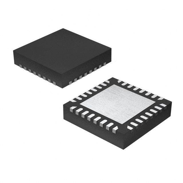
| 描述 | IC RF DSA 7BIT 50 OHM 24-QFN |
| 产品分类 | |
| 品牌 | Peregrine Semiconductor |
| 数据手册 | |
| 产品图片 |
|
| 产品型号 | PE43702MLI-Z |
| rohs | 无铅 / 符合限制有害物质指令(RoHS)规范要求 |
| 产品系列 | UltraCMOS®,HaRP™ |
| 其它名称 | 1046-1047-1 |
| 功率(W) | - |
| 容差 | ±0.3dB |
| 封装/外壳 | 24-VFQFN 裸露焊盘 |
| 标准包装 | 1 |
| 衰减值 | 31.75dB |
| 阻抗 | 50 欧姆 |
| 频率范围 | 9kHz ~ 4GHz |


- 商务部:美国ITC正式对集成电路等产品启动337调查
- 曝三星4nm工艺存在良率问题 高通将骁龙8 Gen1或转产台积电
- 太阳诱电将投资9.5亿元在常州建新厂生产MLCC 预计2023年完工
- 英特尔发布欧洲新工厂建设计划 深化IDM 2.0 战略
- 台积电先进制程称霸业界 有大客户加持明年业绩稳了
- 达到5530亿美元!SIA预计今年全球半导体销售额将创下新高
- 英特尔拟将自动驾驶子公司Mobileye上市 估值或超500亿美元
- 三星加码芯片和SET,合并消费电子和移动部门,撤换高东真等 CEO
- 三星电子宣布重大人事变动 还合并消费电子和移动部门
- 海关总署:前11个月进口集成电路产品价值2.52万亿元 增长14.8%


PDF Datasheet 数据手册内容提取
Product Specification PE43702 50 Ω RF Digital Attenuator Product Description 7-bit, 31.75 dB, 9 kHz - 4.0 GHz Features The PE43702 is a HaRP™-enhanced, high linearity, 7-bit RF Digital Step Attenuator (DSA). This highly versatile DSA HaRP™-enhanced UltraCMOS™ device covers a 31.75 dB attenuation range in 0.25 dB steps. The E Attenuation: 0.25 dB steps to 31.75 dB Peregrine 50Ω RF DSA provides both a serial and parallel CMOS control interface. It maintains high attenuation accuracy High Linearity: Typical +57 dBm IIP3 over frequency and temperature and exhibits very low insertion Excellent low-frequency performance T loss and low power consumption. Performance does not 3.3 V or 5.0 V Power Supply Voltage change with V due to on-board regulator. This next DD generation Peregrine DSA is available in a 4x4 mm 24 lead Fast switch settling time QFN footprint. EProgramming Modes: 1 The PE43702 is manufactured on Peregrine’s UltraCMOS™ Direct Parallel 1 process, a patented variation of silicon-on-insulator (SOI) Latched Parallel technology on a sapphire substrate, offering the performance Serial 7 L of GaAs with the economy and integration of conventional High-attenuation state @ power-up (PUP) 3 CMOS. CMOS Compatible 4 O No DC blocking capacitors required Figure 1. Package Type E 24-lead 4x4x0.85 mm QFN Package Packaged in a 24-lead 4x4x0.85 mm QFN P S H T B I W Figure 2. FunctionaOl Schematic Diagram E RF Input RF Output C Parallel Control A 7 Serial In L Control Logic Interface P CLK E LE R P/S Document No. 70-0244-04 │ www.psemi.com ©2008-2009 Peregrine Semiconductor Corp. All rights reserved. Page 1 of 11 Logo updated under non-rev change. Peregrine products are protected under one or more of the following U.S. Patents: http://patents.psemi.com
PE43702 Product Specification Table 1. Electrical Specifications @ +25°C, V = 3.3 V or 5.0 V DD Parameter Test Conditions Frequency Min Typical Max Units Frequency Range 9 kHz 4.0 GHz Attenuation Range 0.25 dB Step 0 – 31.75 dB Insertion Loss 9 kHz - 4 GHz 2.0 2.5 dB E 0 dB - 7.75 dB Attenuation settings 9 kHz - 4 GHz ±(0.2 + 3%) dB Attenuation Error 8 dB - 31.75 dB Attenuation settings 9 kHz - 4 GHz ±(0.3 + 4%) dB Return Loss 9 kHz - 4 GHz 18 dB Relative Phase All States 9 kHz - 4 GHz 44 deg T P1dB (note 1) Input 20 MHz - 4 GHz 30 32 dBm IIP3 Two tones at +18 dBm, 20 MHz spacing 20 MHz - 4 GHz 57 dBm Typical Spurious Value 1MHz -110 dBm E Video Feed Through 10 1 mVpp Switching Time 50% DC CTRL to 10% / 90% RF 650 ns 1 RF Trise/Tfall 10% / 90% RF 400 ns 7 RF settled to within 0.05 dB of final value. L Settling Time 4 µs RBW = 5 MHz, Averaging ON. 3 Note 1. Please note Maximum Operating Pin (50Ω) of +23dBm as shown in Table 3. 4 O Performance Plots E Figure 3. 0.25dB Step Error vs. Frequency* Figure 4. 0.25dB Attenuation vs. Attenuation State 200 MHz 900 MHz 1800 MHz P PE43702 Attenuation 2200 MHz 3000 MHz 4000 MHz 1 35 S 900 MHz 30 2200 MHz 0.75 H 3800 MHz B 25 Step Error (dB) 00.2.55 B IT Attenuation d 112050 0 W 5 -0.25 O 0 0 4 8 12 16 20 24 28 32 0 5 10 15 20 25 30 35 Attenuation Setting (dB) E Attenuation State *Monotonicity is held so long as Step-Error does not cross below -0.25 C Figure 5. 0.25dB Major State Bit Error Figure 6. 0.25dB Attenuation Error vs. Frequency 0.25dB 0.5dB 1dBA 2dB 200MHz 900MHz 1800MHz 1.5 4dB 8dB 16dB 31.75dB 2200MHz 3000MHz 4000MHz 1.5 L 1 1 Bit Error (dB) -00..550 E P Attenuation Error (dB) -00..505 R -1 -1 -1.5 -1.5 0 500 1000 1500 2000 2500 3000 3500 4000 0 4 8 12 16 20 24 28 32 Frequency (MHz) Attenuation Setting (dB) ©2008-2009 Peregrine Semiconductor Corp. All rights reserved. Document No. 70-0244-04 │ UltraCMOS™ RFIC Solutions Page 2 of 11 Logo updated under non-rev change. Peregrine products are protected under one or more of the following U.S. Patents: http://patents.psemi.com
PE43702 Product Specification Figure 7. Insertion Loss vs. Temperature Figure 8. Input Return Loss vs. Attenuation @ T = +25C 0dB 0.25dB 0.5dB 1dB 2dB -40C +25C +85C 4dB 8dB 16dB 31.75dB 0 0 -0.5 -5 Insertion Loss (dB) --21.-.-5251 nput Return Loss (dB) -----3221105050 T E I -3 -35 -3.5 -40 0 1 2 3 4 5 6 7 8 9 0 1 2 3 4 5 6 7 8 9 Frequency (GHz) E Frequency (GHz) 1 1 7 Figure 9. Output Return Loss vs. Attenuation FigLure 10. Relative Phase vs. Frequency @ T = +25C 3 0dB 0.25dB 0.5dB 1dB 2dB 0dB 0.25dB 0.5dB 1dB 2dB 0 4dB 8dB 16dB 31.75dB O 140 4dB 8dB4 16dB 31.75dB -5 g) 120 E Return Loss (dB) ----22115050 S Phase Error (De 1068000 P Input --3350 Relative 2400H -40 T B -45 0 0 1 2 3 4 5 6 7 8 9 I 0 2 4 6 8 Frequency (GHz) W Frequency (GHz) Figure 11. AttenuaOtion Error vs. Temperature Figure 12. Input IP3 vs. Frequency @ 4 GHz E -40C +25C +85C 0dB 0.25dB 0.5dB 1dB 2dB 1.5 70 4dB 8dB 16dB 31.75dB C 65 1 or (dB) 0.5 A Bm)5650 enuation Err -0.50 P L nput IP3 (d4550 Att I40 -1 35 E -1.5 30 0 4 8 12 16 20 24 28 32 0 500 1000 1500 2000 2500 3000 3500 4000 4500 R Attenuation Setting (dB) Frequency (MHz) Document No. 70-0244-04 │ www.psemi.com ©2008-2009 Peregrine Semiconductor Corp. All rights reserved. Page 3 of 11 Logo updated under non-rev change. Peregrine products are protected under one or more of the following U.S. Patents: http://patents.psemi.com
PE43702 Product Specification Figure 13. Pin Configuration (Top View) Table 3. Operating Ranges 5 C 0. C1 C2 C4 C8 C16 Parameter Min Typ Max Units V Power Supply Voltage 3.0 3.3 V 24 23 22 21 20 19 DD V Power Supply Voltage 5.0 5.5 V C0.25 1 18 SI DD I Power Supply Current 50 350 μA VDD 2 17 CLK DD Exposed Digital Input High 2.6 E 5.5 V P/S 3 Solder 16 LE P Input power (50Ω): GND 4 Pad 15 GND IN 9 kHz ≤ 20 MHz Fig. 14 dBm RF1 5 14 RF2 20 MHz ≤ 4 GHz +23 dBm GND 6 13 GND TOP Operating temperature ranTge -40 25 85 °C 7 8 9 10 11 12 Digital Input Low 0 1 V D D D D D D N N N N N N Digital Input Leakage1 15 μA G G G G G G Note 1. Input leakage current per Control pin E Table 2. Pin Descriptions 1 Table 4. Absolute Maximum Ratings Pin No. Pin Name Description 1 1 C0.25 (D0) Attenuation control bit, 0.25 dB Symbol Parameter/Conditions Min Max Units 2 V Power supply pin V Power supply voltage 7-0.3 6.0 V DD LDD 3 P(cid:3636)/S Serial/Parallel mode select V Voltage on any Digital input -0.3 5.8 V I 3 4 GND Ground T Storage temperature range -65 150 °C ST 5 RF1 RF1 port Input power (50Ω) 4 6 - 13 GND Ground O P 9 kHz ≤ 20 MHz Fig. 14 dBm IN 14 RF2 RF2 port 20 MHz ≤ 4 GHz +23 dBm E 15 GND Ground ESD voltage (HBM)1 500 V V ESD ESD voltage (Machine Model) 100 V 16 LE Serial interface Latch Enable input 17 CLK Serial interface Clock input Note: 1. Human PBody Model (HBM, MIL_STD 883 Method 3015.7) 18 SI Serial interface Data input S Exceeding absolute maximum ratings may cause 19 C16 (D6) Parallel control bit, 16 dB permaHnent damage. Operation should be restricted to 20 C8 (D5) Parallel control bit, 8 dB the limits in the Operating Ranges table. Operation 21 C4 (D4) Parallel control bit, 4 dB between operating range maximum and absolute 22 C2 (D3) Parallel control bit, 2 dB T B maximum for extended periods may reduce reliability. 23 C1 (D2) Parallel control bit, 1 dB 24 C0.5 (D1) Parallel control bit, 0.5 dB IFigure 14. Maximum Power Handling Capability Paddle GND Ground for proper operation W Note: Ground C0.25, C0.5, C1, C2, C4, C8, C16 if not in use. 30.0 O 25.0 Exposed Solder Pad Connection E 20.0 The exposed solder pad on the bottom of the package m) B must be grounded for proper device operaCtion. n (d 15.0 Pi 10.0 Moisture Sensitivity Level A 5.0 The Moisture Sensitivity Level rating for the PE43702 in the 24-lead 4x4 QFN package is MSL1. 0.0 L 1.0E+03 1.0E+04 1.0E+05 1.0E+06 1.0E+07 1.0E+08 1.0E+09 Hz Switching Frequency P The PE43702 has a maximum 25 kHz switching rate. Electrostatic Discharge (ESD) Precautions Switching rate is deEfined to be the speed at which the When handling this UltraCMOS™ device, observe the DSA can be toggled across attenuation states. same precautions that you would use with other ESD- R sensitive devices. Although this device contains Latch-Up Avoidance circuitry to protect it from damage due to ESD, Unlike conventional CMOS devices, UltraCMOS™ precautions should be taken to avoid exceeding the devices are immune to latch-up. specified rating. ©2008-2009 Peregrine Semiconductor Corp. All rights reserved. Document No. 70-0244-04 │ UltraCMOS™ RFIC Solutions Page 4 of 11 Logo updated under non-rev change. Peregrine products are protected under one or more of the following U.S. Patents: http://patents.psemi.com
PE43702 Product Specification Table 5. Control Voltage Table 9. Serial Attenuation Word Truth Table State Bias Condition Attenuation Word Attenuation Low 0 to +1.0 Vdc at 2 µA (typ) D0 Setting D7 D6 D5 D4 D3 D2 D1 RF1-RF2 (LSB) High +2.6 to +5 Vdc at 10 µA (typ) L L L L L L L L Reference I.L. E L L L L L L L H 0.25 dB Table 6. Latch and Clock Specifications L L L L L L H L 0.5 dB L L L L L H L L 1 dB Latch Enable Shift Clock Function L L L L HT L L L 2 dB 0 ↑ Shift Register Clocked L L L H L L L L 4 dB Contents of shift register ↑ X transferred to attenuator core L L H L L L L L 8 dB L H L EL L L L L 116 dB Table 7. Parallel Truth Table L H H H H H H H 31.75 dB 1 Parallel Control Setting Attenuation Setting 7 D6 D5 D4 D3 D2 D1 D0 RF1-RF2 L 3 L L L L L L L Reference I.L. L L L L L L H 0.25 dB 4 O L L L L L H L 0.5 dB E L L L L H L L 1 dB L L L H L L L 2 dB P L L H L L L L S4 dB L H L L L L L 8 dB H H L L L L L L 16 dB H H H H H H H 31.75 dB T B I W Table 8. Serial Register Map O MSB (last in) LSB (first in) E Q7 Q6 Q5 Q4 Q3 Q2 Q1 Q0 Bit must be set to logic low C D7 D6 D5 D4 D3 D2 D1 D0 A Attenuation Word L Attenuation Word is derived directly from the attenuation value. For example, to program the 12.5 dB state: P Attenuation Word: Multiply by 4 and convert to binary → 4 * 12.5 dB → 50 → 00110010 E Serial Input: 00110010 R Document No. 70-0244-04 │ www.psemi.com ©2008-2009 Peregrine Semiconductor Corp. All rights reserved. Page 5 of 11 Logo updated under non-rev change. Peregrine products are protected under one or more of the following U.S. Patents: http://patents.psemi.com
PE43702 Product Specification Programming Options LOW to prevent the attenuator value from changing Parallel/Serial Selection as data is entered. The LE input should then be Either a parallel or serial interface can be used to toggled HIGH and brought LOW again, latching the control the PE43702. The P(cid:3636)/S bit provides this new data into the DSA. Attenuation Word truth table is listed in Table 9. A programming example of the selection, with P(cid:3636)/S=LOW selecting the parallel serial register is illustrated in Table 8. The serial interface and P(cid:3636)/S=HIGH selecting the serial E timing diagram is illustrated in Fig. 15. It is required interface. that all parallel pins be grounded when the DSA is used in serial mode. Parallel Mode Interface The parallel interface consists of seven CMOS- Power-up Control SeTttings compatible control lines that select the desired The PE43702 will always initialize to the maximum attenuation state, as shown in Table 7. attenuation setting (31.5 dB) on power-up for both the serial and latched-parallel modes of operation The parallel interface timing requirements are E and will remain in this setting until the use1r latches in defined by Fig. 16 (Parallel Interface Timing the next programming word. In direct-parallel mode, Diagram), Table 11 (Parallel Interface AC 1 the DSA can be preset to any state within the 31.5 Characteristics), and switching speed (Table 1). dBL range by pre-setting the para7llel control pins prior to power-up. In this mode, there is a 400-µs delay For latched-parallel programming the Latch Enable between the time the DSA is3 powered-up to the time (LE) should be held LOW while changing attenuation the desired state is set. During this power-up delay, state control values, then pulse LE HIGH to LOW 4 O the device attenuates to the maximum attenuation (per Fig. 16) to latch new attenuation state into setting (31.5 dB) before defaulting to the user device. E defined state. If the control pins are left floating in this mode during power-up, the device will default to For direct parallel programming, the Latch Enable P the minimum attenuation setting (insertion loss (LE) line should be pulled HIGH. Changing S state). attenuation state control values will change device state to new attenuation. Direct Mode is ideal for H Dynamic operation between serial and parallel manual control of the device (using hardwire, programming modes is possible. switches, or jumpers). T B If the DSA powers up in serial mode (P(cid:3636)/S = HIGH), Serial Interface I all the parallel control inputs DI[6:0] must be set to The serial interface is a 8-bit serial-in, parallel-out W logic low. Prior to toggling to parallel mode, the DSA shift register buffered by a transparent latch. The 8- O must be programmed serially to ensure D[7] is set to bits make up the Attenuation Word that controls the logic low. DSA. Fig. 15 illustrates a example timing diagra m for E programming a state. If the DSA powers up in either latched or direct- C parallel mode, all parallel pins DI[6:0] must be set to The serial-interface is controlled using three CMOS- logic low prior to toggling to serial mode (P(cid:3636)/S compatible signals: Serial-In (SI), Clock (CLK), and = HIGH), and held low until the DSA has been Latch Enable (LE). The SI and CALK inputs allow programmed serially to ensure bit D[7] is set to logic data to be serially entered into the shift register. low. Serial data is clocked in LSBL first. P The sequencing is only required once on power- The shift register must be loaded while LE is held up. Once completed, the DSA may be toggled E between serial and parallel programming modes at will. R ©2008-2009 Peregrine Semiconductor Corp. All rights reserved. Document No. 70-0244-04 │ UltraCMOS™ RFIC Solutions Page 6 of 11 Logo updated under non-rev change. Peregrine products are protected under one or more of the following U.S. Patents: http://patents.psemi.com
PE43702 Product Specification Figure 15. Serial Timing Diagram Bits can either be set to logic high or logic low D[7] must be set to logic low DI[6:0] TDISU TDIH P/S E TPSSU TPSIH SI D[0] D[1] D[2] D[3] D[4] D[5] D[6] D[7] TSISU TSIH CLK T TCLKL TCLKH TLESU LE TLEPW TPD DO[6:0] EVALID 1 Figure 16. Latched-Parallel/Direct-Parallel Timing Diagram 1 P/S 7 L T T PSSU PSH 3 DI[6:0] VALID T 4 DISU O T DIH E LE T LEPW P DO[6:0] VALID S T PD TDIPD H Table 10. Serial Interface ACB Characteristics TTable 11. Parallel and Direct Interface AC V = 3.3 or 5.0 V, -40° C < T < 85° C, unless otherwise specified Characteristics DD A I Symbol Parameter Min Max Unit W VDD = 3.3 or 5.0 V, -40° C < TA < 85° C, unless otherwise specified FCLK Serial clock freOquency - 10 MHz Symbol Parameter Min Max Unit TCLKH Serial clock HIGH time 30 - ns Latch Enable minimum T 30 - ns T Serial clock LOW time 30 - E ns LEPW pulse width CLKL T Parallel data setup time 100 - ns Last serial clock rising edge DISU T setup time to Latch Enable 10 C - ns LESU T Parallel data hold time 100 - ns rising edge DIH T Latch Enable min. pulse width A 30 - ns TPSSU Parallel/Serial setup time 100 - ns LEPW TSISU Serial data setup time 10 - ns TPSIH Parallel/Serial hold time 100 - ns L TSIH Serial data hold time 10 - ns T Digital register delay - 10 ns PD (internal) TDISU Parallel data setupP time 100 - ns Digital register delay T Parallel data hold time 100 - ns T - 5 ns DIH DIPD (internal, direct mode only) T Address seEtup time 100 - ns ASU T Address hold time 100 - ns AH R T Parallel/Serial setup time 100 - ns PSSU T Parallel/Serial hold time 100 - ns PSH T Digital register delay (internal) - 10 ns PD Document No. 70-0244-04 │ www.psemi.com ©2008-2009 Peregrine Semiconductor Corp. All rights reserved. Page 7 of 11 Logo updated under non-rev change. Peregrine products are protected under one or more of the following U.S. Patents: http://patents.psemi.com
PE43702 Product Specification Evaluation Kit Figure 17. Evaluation Board Layout Peregrine Specification 101-0310 The Digital Attenuator Evaluation Kit board was designed to ease customer evaluation of the PE43702 Digital Step Attenuator. Direct-Parallel Programming Procedure E For automated direct-parallel programming, connect the test harness provided with the EVK from the parallel port of the PC to the J1 & Serial header pin and set the D0-D6 SP3T switches to T the ‘MIDDLE’ toggle position. Position the Parallel/Serial (P(cid:3636)/S) select switch to the Parallel (or left) position. The evaluation software is E written to operate the DSA in either Parallel or 1 Serial-Addressable Mode. Ensure that the 1 software is set to program in Direct-Parallel mode. Using the software, enable or disable each setting 7 L to the desired attenuation state. The software automatically programs the DSA each time an 3 attenuation state is enabled or disabled. 4 O For manual direct-parallel programming, E disconnect the test harness provided with the EVK from the J1 and Serial header pins. Position the P Parallel/Serial (P(cid:3636)/S) select switch to the Parallel S (or left) position. The LE pin on the Serial header must be tied to V . Switches D0-D6 are SP3T H DD switches which enable the user to manually program the parallel bits. When any input D0-D6 T B Note: Reference Figure 18 for Evaluation Board Schematic is toggled ‘UP’, logic high is presented to the parallel input. When toggled ‘DOWN’, logic low is I presented to the parallel input. Setting D0-D6 to W as the parallel bits are applied. The user must the ‘MIDDLE’ toggle position presents an OPEN, then pulse LE from 0V to VDD and back to 0V to O which forces an on-chip logic low. Table 9 depicts latch the programming word into the DSA. LE the parallel programming truth table and Fig. 16 must be logic low prior to programming the next E illustrates the parallel programming timing word. diagram. C Serial Programming Procedure Latched-Parallel Programming Procedure Position the Parallel/Serial (P(cid:3636)/S) select switch to A For automated latched-parallel programming, the the Serial (or right) position. The evaluation procedure is identical to the direct-parallel software is written to operate the DSA in either L method. The user only must ensure that Latched- Parallel or Serial Mode. Ensure that the software Parallel is selected in tPhe software. is set to program in Serial mode. Using the software, enable or disable each setting to the For manual latcheEd-parallel programming, the desired attenuation state. The software procedure is identical to direct-parallel except now automatically programs the DSA each time an the LE pin oRn the Serial header must be logic low attenuation state is enabled or disabled. ©2008-2009 Peregrine Semiconductor Corp. All rights reserved. Document No. 70-0244-04 │ UltraCMOS™ RFIC Solutions Page 8 of 11 Logo updated under non-rev change. Peregrine products are protected under one or more of the following U.S. Patents: http://patents.psemi.com
PE43702 Product Specification Figure 18. Evaluation Board Schematic Peregrine Specification 102-0379 VDD 4 6 1 2 4 1 2 4 1 2 4 1 2 4 1 2 4 1 2 4 1 2 4 P/S D0 D1 D2 D3 D4 D5 D6 5 3 3 3 3 3 3 3 E P/S D0 D1 D2 D3 D4 D5 D6 J1 HEADER 14 1110242468 2468111024 113113579 135719131 DDDDDDD0123456 T 1C050pF 1C060pF C1070pF D1 D2 D3 D4 D5 D6 E SHEERAIDALER 4 1 JC3ON2 VDD 1C010pF 1C020pF 1C030pF C1040pF D0 1 CP2524CP523C122C221C420C819C16 SI 18 DCLALETKA 1234 DLGCENALTDOACK 1 12 0C.19µF C10100pF 1C080pF 1C0103pF 1C0104pF VPD/SD 2345 VSGR/FDNP1DD43X0X DSA 50 OUhm1 L4x4 MLP24 GCRNLFLKDE2 11114567 SMJA53 7 JS4MA 1 Z=50 Ohm 6 GNDGND GND GND GND GND GNDGND 13 Z=50 Ohm 41 2 O JS6MA De-emZb=e5d0in Ogh tmrace SMJA7 2 7 8 9 10 11 12 1 1 E 2 2 Note: Capacitors C1-C8, C13, & C14 may be omitted. P Figure 19. Package Drawing S H T B I W O E C A L P E R Document No. 70-0244-04 │ www.psemi.com ©2008-2009 Peregrine Semiconductor Corp. All rights reserved. Page 9 of 11 Logo updated under non-rev change. Peregrine products are protected under one or more of the following U.S. Patents: http://patents.psemi.com
PE43702 Product Specification Figure 20. Tape and Reel Drawing E T E 1 1 Tape Feed Direction 7 L Pin 1 3 A0 = 4.35 Top of B0 = 4O.35 4 Device K = 1.1 0 E PDevice Orientation in Tape S H Figure 21. Marking Specifications T B I W 43702 O YYWW EYYWW = Date Code ZZZZZ = Last five digits of Lot Number ZZZZZ C A L P Table 12. Ordering Information E Order Code Part Marking Description Package Shipping Method R PE43702MLI 43702 PE43702 G - 24QFN 4x4mm-75A Green 24-lead 4x4mm QFN Bulk or tape cut from reel PE43702MLI-Z 43702 PE43702 G – 24QFN 4x4mm-3000C Green 24-lead 4x4mm QFN 3000 units / T&R EK43702-01 43702 PE43702 G – 24QFN 4x4mm-EK Evaluation Kit 1 / Box ©2008-2009 Peregrine Semiconductor Corp. All rights reserved. Document No. 70-0244-04 │ UltraCMOS™ RFIC Solutions Page 10 of 11 Logo updated under non-rev change. Peregrine products are protected under one or more of the following U.S. Patents: http://patents.psemi.com
PE43702 Product Specification Sales Offices The Americas Peregrine Semiconductor Corporation Peregrine Semiconductor, Asia Pacific (APAC) 9380 Carroll Park Drive Shanghai, 200040, P.R. China San Diego, CA 92121 Tel: +86-21-5836-8276 E Fax: +86-21-5836-7652 Tel: 858-731-9400 Fax: 858-731-9499 Peregrine Semiconductor, Korea #B-2607, Kolon Tripolis, 210 Europe Geumgok-dong, Bundang-gTu, Seongnam-si Gyeonggi-do, 463-943 South Korea Peregrine Semiconductor Europe Tel: +82-31-728-3939 Bâtiment Maine Fax: +82-31-728-3940 13-15 rue des Quatre Vents Peregrine SEemiconductor K.K., Japan 1 F-92380 Garches, France Teikoku Hotel Tower 10B-6 Tel: +33-1-4741-9173 1-1-1 Uchisaiwai-cho, Chiyoda-ku 1 Fax : +33-1-4741-9173 Tokyo 100-0011 Japan Tel: +81-3-3502-5211 7 L High-Reliability and Defense Products Fax: +81-3-3502-5213 3 Americas San Diego, CA, USA 4 Phone: 858-731-9475 O Fax: 848-731-9499 E Europe/Asia-Pacific Aix-En-Provence Cedex 3, France P Phone: +33-4-4239-3361 S Fax: +33-4-4239-7227 H For a list of representatives in your area, please refer to our Web site at: www.psemi.com T B Data Sheet Identification I W Advance Information The information in this data sheet is believed to be reliable. O However, Peregrine assumes no liability for the use of this The product is in a formative or design stage. The data information. Use shall be entirely at the user’s own risk. sheet contains design target specifications for produEct development. Specifications and features may change in No patent rights or licenses to any circuits described in this any manner without notice. C data sheet are implied or granted to any third party. Preliminary Specification A Peregrine’s products are not designed or intended for use in The data sheet contains preliminary data. Additional data devices or systems intended for surgical implant, or in other may be added at a later date. PeLregrine reserves the right applications intended to support or sustain life, or in any to change specifications at any time without notice in order application in which the failure of the Peregrine product could to supply the best possible Pproduct. create a situation in which personal injury or death might occur. Peregrine assumes no liability for damages, including Product SpecificEation consequential or incidental damages, arising out of the use of its products in such applications. The data sheetR contains final data. In the event Peregrine decides to change the specifications, Peregrine will notify The Peregrine name, logo, and UTSi are registered trademarks customers of the intended changes by issuing a CNF and UltraCMOS, HaRP, MultiSwitch and DuNE are trademarks (Customer Notification Form). of Peregrine Semiconductor Corp. Document No. 70-0244-04 │ www.psemi.com ©2008-2009 Peregrine Semiconductor Corp. All rights reserved. Page 11 of 11 Logo updated under non-rev change. Peregrine products are protected under one or more of the following U.S. Patents: http://patents.psemi.com