ICGOO在线商城 > 射频/IF 和 RFID > 衰减器 > PE4312MLBA-Z

 Datasheet下载
- 型号: PE4312MLBA-Z
- 制造商: Peregrine
- 库位|库存: xxxx|xxxx
- 要求:
| 数量阶梯 | 香港交货 | 国内含税 |
| +xxxx | $xxxx | ¥xxxx |
查看当月历史价格
查看今年历史价格
PE4312MLBA-Z产品简介:
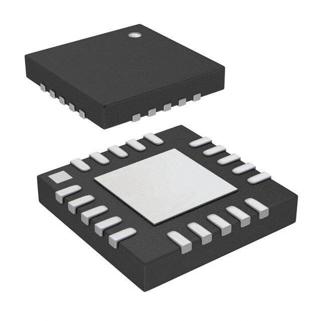
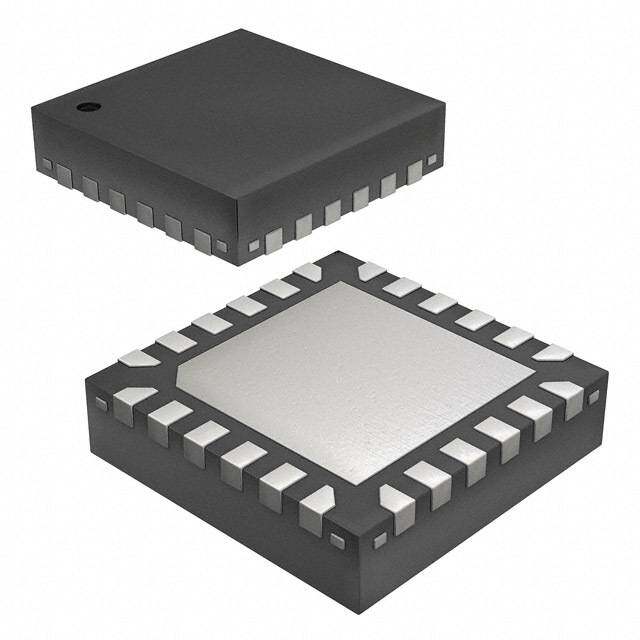
ICGOO电子元器件商城为您提供PE4312MLBA-Z由Peregrine设计生产,在icgoo商城现货销售,并且可以通过原厂、代理商等渠道进行代购。 PE4312MLBA-Z价格参考。PeregrinePE4312MLBA-Z封装/规格:衰减器, RF Attenuator 31.5dB ±0.15dB 0Hz ~ 4GHz 50 Ohms 20-VFQFN Exposed Pad。您可以下载PE4312MLBA-Z参考资料、Datasheet数据手册功能说明书,资料中有PE4312MLBA-Z 详细功能的应用电路图电压和使用方法及教程。
pSemi(现为Qorvo旗下品牌)的PE4312MLBA-Z是一款数字控制硅基衰减器,广泛应用于需要精确信号电平调节的射频系统中。该器件支持31 dB的衰减范围,步进为0.5 dB,具备高精度和良好的线性特性,适用于工作频率高达4 GHz的场景。

典型应用场景包括:无线通信基础设施,如5G小基站和宏基站中的发射/接收链路功率控制;测试与测量设备,用于自动增益校准和信号调理;宽带通信系统和射频前端模块,实现动态信号调节;以及航空航天与国防领域的雷达和电子战系统,提供可靠的射频信号管理。

PE4312MLBA-Z采用紧凑的6引脚MCM封装,具有低插入损耗、高功率耐受能力和出色的温度稳定性,适合在严苛环境中使用。其无需负电压供电的设计简化了电源架构,提升了系统集成便利性,是现代高性能射频系统中理想的数字衰减解决方案。
| 参数 | 数值 |
| 产品目录 | |
| 描述 | IC DGTL ATTEN 31.5DB 6BIT 20QFN |
| 产品分类 | |
| 品牌 | Peregrine Semiconductor |
| 数据手册 | |
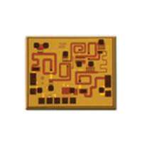
| 产品图片 |
|
| 产品型号 | PE4312MLBA-Z |
| rohs | 无铅 / 符合限制有害物质指令(RoHS)规范要求 |
| 产品系列 | UltraCMOS®,HaRP™ |
| 其它名称 | 1046-1098-1 |
| 功率(W) | - |
| 容差 | ±0.15dB |
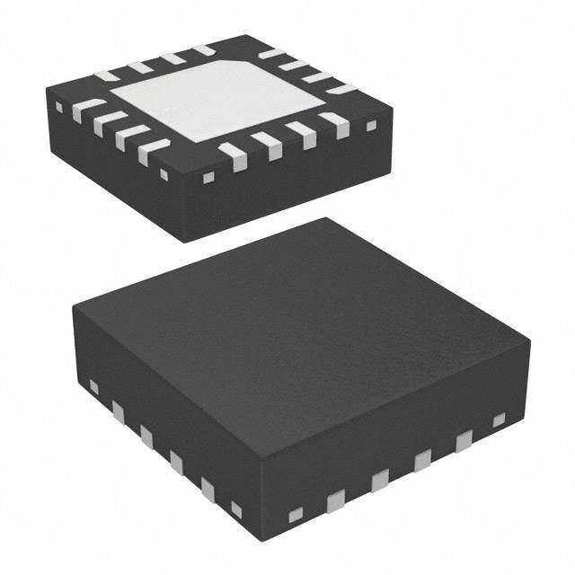
| 封装/外壳 | 20-VFQFN 裸露焊盘 |
| 标准包装 | 1 |
| 衰减值 | 31.5dB |
| 配用 | /product-detail/zh/EK4312-11/1046-1097-ND/4780772 |
| 阻抗 | 50 欧姆 |
| 频率范围 | 0 ~ 4GHz |


- 商务部:美国ITC正式对集成电路等产品启动337调查
- 曝三星4nm工艺存在良率问题 高通将骁龙8 Gen1或转产台积电
- 太阳诱电将投资9.5亿元在常州建新厂生产MLCC 预计2023年完工
- 英特尔发布欧洲新工厂建设计划 深化IDM 2.0 战略
- 台积电先进制程称霸业界 有大客户加持明年业绩稳了
- 达到5530亿美元!SIA预计今年全球半导体销售额将创下新高
- 英特尔拟将自动驾驶子公司Mobileye上市 估值或超500亿美元
- 三星加码芯片和SET,合并消费电子和移动部门,撤换高东真等 CEO
- 三星电子宣布重大人事变动 还合并消费电子和移动部门
- 海关总署:前11个月进口集成电路产品价值2.52万亿元 增长14.8%
PDF Datasheet 数据手册内容提取
Product Specification PE4312 UltraCMOS® RF Digital Step Attenuator - 6 bit, 31.5 dB, 1 MHz–4 GHz Product Description The PE4312 is a 50Ω, HaRP™ technology-enhanced 6-bit Features RF Digital Step Attenuator (DSA) designed for use in 3G/4G Attenuation: 0.5 dB steps to 31.5 dB wireless infrastructure and other high performance RF applications. Safe attenuation state transitions - Monotonicity: 0.5 dB up to 4 GHz This DSA is a pin compatible upgraded version of the PE4302 with higher linearity, improved attenuation accuracy High attenuation accuracy and faster switching speed. An integrated digital control ±(0.10 + 1% x Atten) @ 1 GHz interface supports both serial and parallel programming of ±(0.15 + 2% x Atten) @ 2.2 GHz the attenuation, including the capability to program an initial - ±(0.15 + 8% x Atten) @ 4 GHz attenuation state at power up. High linearity: +59 dBm IIP3 Covering a 31.5 dB attenuation range in 0.5 dB steps, it Wide power supply range of 2.3–5.5V maintains high linearity and low power consumption from 1 MHz through 4 GHz. PE4312 also features an external 1.8V control logic compatible negative supply option, and is offered in a 20-lead 4 × 4 mm 105 °C operating temperature QFN package. In addition, no external blocking capacitors Programming modes are required if 0 VDC is present on the RF ports. Direct parallel The PE4312 is manufactured on Peregrine’s UltraCMOS® Latched parallel - - process, a patented variation of silicon on insulator (SOI) Serial technology on a sapphire substrate. Unique power-up state selection Peregrine’s HaRP™ technology enhancements deliver high Pin compatible to PE4302, PE4305 linearity and excellent harmonics performance. It is an and PE4306 innovative feature of the UltraCMOS® process, offering the performance of GaAs with the economy and integration of conventional CMOS. Figure 2. Package Type - 20 lead 4 × 4 mm QFN Figure 1. Functional Schematic Diagram Switched Attenuator Array RF Input RF Output Parallel Control 6 Control Logic Interface Serial Control 3 Power-Up Control 2 DOC-02132 Document No. DOC-81482-2 │www.psemi.com ©2017 Peregrine Semiconductor Corp. All rights reserved. Page 1 of 13
PE4312 Product Specification Table 1. Electrical Specifications @ 25 °C (Z = Z = 50Ω), unless otherwise noted S L Normal Mode1: V = 3.3V, V = 0V or Bypass Mode2: V = 3.3V, V = –3.3V DD SS_EXT DD SS_EXT Parameter Condition Frequency Min Typ Max Unit Operation frequency 1 4000 MHz Attenuation range 0.5 dB step 0–31.5 dB 1 MHz–<1 GHz 1.3 1.5 dB Insertion loss 1–2.2 GHz 1.5 1.8 dB 2.2–4 GHz 2.1 2.3 dB 1 MHz–1 GHz ±(0.10 + 1% of atten setting) dB Attenuation error Any bit or bit combination 1–<2.2 GHz ±(0.15 + 2% of atten setting) dB 2.2–4 GHz ±(0.15 + 8% of atten setting) dB R(ineptuurtn o lro osus t put port) 12.–22–.24 GGHHzz 1140 1187 dB Input 0.1dB compression point3 1 MHz–4 GHz 30 dBm Input IP3 Two tones at +18 dBm, 10 kHz spacing 1950 MHz 59 dBm Switching time 50% CTRL to 90% or 10% RF 500 800 ns Notes: 1. Normal mode: single external positive supply used. 2. Bypass mode: both external positive supply and external negative supply used. 3. The input 0.1dB compression point is a linearity figure of merit. Refer to Table 5 for the operating RF input power (50Ω). ©2017 Peregrine Semiconductor Corp. All rights reserved. Document No. DOC-81482-2 │ UltraCMOS® RFIC Solutions Page 2 of 13
PE4312 Product Specification Figure 3. Pin Configuration (Top View) Table 3. Operating Ranges Pmianr 1ki ndgo t 0.5 1 ND 2 4 Parameter Symbol Min Typ Max Unit C C G C C Normal mode1 20 19 18 17 16 Supply voltage V 2.3 5.5 V DD Supply current I 130 200 μA C16 1 15 C8 DD Bypass mode2 RF1 2 14 RF2 Exposed Supply voltage V 2.7 5.5 V Data 3 Ground Pad 13 P/S DD Supply current I 50 80 μA Clock 4 12 VSS_EXT/GND DD Negative supply voltage V -3.6 -3.2 V LE 5 11 GND SS_EXT Negative supply current I -40 -16 μA SS 6 7 8 9 10 Normal or Bypass mode D 1 2 D D VD UP UP VD GN Digital input high 1.17 3.6 V P P Digital input low -0.3 0.6 V Table 2. Pin Descriptions Digital input leakage3 20 μA Pin # Pin Name Description RF input power, CW 1 C163,5 Attenuation control bit, 16 dB 1>–5500 M MHHz–z 4 GHz PMAX_CW F+ig2.4 4 ddBBmm 2 RF11 RF1 port (RF input) RF input power, pulsed4 3 Data3 Serial interface data input 1–50 MHz PMAX_PULSED Fig. 4 dBm >50 MHz–4 GHz +27 dBm 4 Clock Serial interface clock input 5 LE4 Latch Enable input Orapnegrea ting temperature TOP -55 +105 °C 6 VDD Supply voltage (nominal 3.3V) Notes: 1. Normal mode: connect pin 12 to GND to enable internal negative 7 PUP15 Power-up selection bit 1 v2o. lBtaygpea sgse nmeoradteo:r a. pply a negative voltage to VSS_EXT (pin 12) to bypass 8 PUP2 Power-up selection bit 2 and disable internal negative voltage generator. 3. Applies to all pins except pins 1, 5, 7 and 20. Pins 1, 7 and 20 have 9 V Supply voltage (nominal 3.3V) an internal pull-down resistor and pin 5 has an internal pull-up resistor. DD 4. Pulsed, 5% duty cycle of 4620 µs period, 50Ω. 10, 11, 18 GND Ground 12 VGSSN_EDX2T / Egrxoteurnnda l VSS negative voltage control or Table 4. Absolute Maximum Ratings 13 P/S Parallel/Serial mode select Parameter Symbol Min Max Unit 14 RF21 RF2 port (RF output) Supply voltage VDD -0.3 5.5 V 15 C8 Attenuation control bit, 8 dB Digital input voltage VCTRL -0.3 3.6 V 16 C4 Attenuation control bit, 4 dB Maximum input power PMAX_ABS +30 dBm 17 C2 Attenuation control bit, 2 dB Storage temperature range TST -65 +150 °C 19 C1 Attenuation control bit, 1 dB ESD voltage HBM*, all pins VESD 1500 V 20 C0.55 Attenuation control bit, 0.5 dB Note: * Human Body Model (MIL-STD-883 Method 3015) Pad GND Exposed pad: ground for proper operation Exceeding absolute maximum ratings may cause Notes: 1. RF pins 2 and 14 must be at 0 VDC. The RF pins do not require DC blocking capacitors for proper operation if the 0 VDC requirement is met. permanent damage. Operation should be 2. Use VSS_EXT (pin 12, refer to Table 3) to bypass and disable internal restricted to the limits in the Operating Ranges negative voltage generator. Connect VSS_EXT (pin 12, VSS_EXT = GND) to enable internal negative voltage generator. table. Operation between operating range 3. Place a 10 kΩ resistor in series, as close to pin as possible to avoid maximum and absolute maximum for extended frequency resonance. 4. This pin has an internal 2 MΩ resistor to internal positive digital supply. periods may reduce reliability. 5. This pin has an internal 200 kΩ resistor to GND. Document No. DOC-81482-2 │www.psemi.com ©2017 Peregrine Semiconductor Corp. All rights reserved. Page 3 of 13
PE4312 Product Specification Electrostatic Discharge (ESD) Precautions Safe Attenuation State Transitions When handling this UltraCMOS device, observe The PE4312 features a novel architecture to the same precautions that you would use with provide safe transition behavior when changing - other ESD sensitive devices. Although this device attenuation states. When RF input power is contains circuitry to protect it from damage due to applied, positive output power spikes are ESD, precautions should be taken to avoid prevented during attenuation state changes by exceeding the rate specified. optimized internal timing control. - Latch Up Avoidance Resistor on Pin 1 & 3 Unlike conventional CMOS devices, UltraCMOS A 10 kΩ resistor on the inputs to pin 1 and 3 (see - devices are immune to latch up. Figure 26) will eliminate package resonance between the RF input pin and the two digital Switching Frequency inputs. Specified attenuation error versus frequency performance is dependent upon this The PE4312 has a maximum 25 kHz switching condition. rate in normal mode (pin 12 = GND). A faster switching rate is available in bypass mode (pin 12 Moisture Sensitivity Level = V ). The rate at which the PE4312 can be SS_EXT switched is then limited to the switching time as The moisture sensitivity level rating for the specified in Table 1. PE4312 in the 4 × 4 mm QFN package is MSL1. Switching frequency describes the time duration Spurious Performance between switching events. Switching time is the - time duration between the point the control signal The typical low frequency spurious performance reaches 50% of the final value and the point the of the PE4312 in normal mode is –140 dBm - output signal reaches within 10% or 90% of its (pin12 = GND). If spur free performance is target value. desired, the internal negative voltage generator can be disabled by applying a negative voltage to V (pin 12). SS_EXT Figure 4. Power Derating Curve for 1–50 MHz 30 28 26 24 22 20 m) B 18 d er ( 16 w o 14 P ut 12 p In 10 8 6 RF Input Power, CW or Pulsed (-40C to 105C) 4 2 0 0 5 10 15 20 25 30 35 40 45 50 Frequency (MHz) ©2017 Peregrine Semiconductor Corp. All rights reserved. Document No. DOC-81482-2 │ UltraCMOS® RFIC Solutions Page 4 of 13
PE4312 Product Specification Programming Options Clock, and Latch Enable (LE). The Data and Clock inputs allow data to be serially entered into the shift Parallel/Serial Selection register, a process that is independent of the state of Either a parallel or serial interface can be used to the LE input. control the PE4312. The P/S bit provides this selection, with P/S = LOW selecting the parallel The LE input controls the latch. When LE is HIGH, interface and P/S = HIGH selecting the serial the latch is transparent and the contents of the serial interface. shift register control the attenuator. When LE is brought LOW, data in the shift register is latched. Parallel Mode Interface - The parallel interface consists of six CMOS The shift register should be loaded while LE is held compatible control lines that select the desired LOW to prevent the attenuator value from changing attenuation state, as shown in Table 5. as data is entered. The LE input should then be toggled HIGH and brought LOW again, latching the The parallel interface timing requirements are new data. The timing for this operation is defined by defined by Figure 5 (Parallel Interface Timing Figure 5 (Serial Interface Timing Diagram) and Diagram), Table9 (Parallel Interface AC Table8 (Serial Interface AC Characteristics). Characteristics), and switching speed (Table 1). - Power up Control Settings For latched parallel programming the Latch Enable The PE4312 always assumes a specifiable (LE) should be held LOW while changing attenuation - attenuation setting on power up. This feature exists state control values, then pulse LE HIGH to LOW for both the Serial and Parallel modes of operation, (per Figure 5) to latch the new attenuation state into and allows a known attenuation state to be the device. established before an initial serial or parallel control word is provided. For direct parallel programming, the Latch Enable (LE) line should be pulled HIGH. Changing When the attenuator powers up in Serial mode attenuation state control values will change device (P/S = 1), the six control bits are set to whatever state to new attenuation. Direct Mode is ideal for data is present on the six parallel data inputs (C0.5 manual control of the device (using hardwire, to C16). This allows any one of the 64 attenuation switches, or jumpers). - settings to be specified as the power up state. Table 5. Truth Table* When the attenuator powers up in Parallel mode (P/S = 0) with LE = 0, the control bits are P/S C16 C8 C4 C2 C1 C0.5 Attenuation State automatically set to one of four possible values. - 0 0 0 0 0 0 0 Reference Loss These four values are selected by the two power up 0 0 0 0 0 0 1 0.5 dB control bits, PUP1 and PUP2, as shown in Table 6 - (Power Up Truth Table, Parallel Mode). 0 0 0 0 0 1 0 1 dB 0 0 0 0 1 0 0 2 dB 0 0 0 1 0 0 0 4 dB Table 6. Parallel PUP Truth Table* 0 0 1 0 0 0 0 8 dB P/S LE PUP2 PUP1 Attenuation State 0 1 0 0 0 0 0 16 dB 0 0 0 0 Reference Loss 0 1 1 1 1 1 1 31.5 dB 0 0 1 0 8 dB Note: * Not all 64 possible combinations of C0.5–C16 are shown in table. 0 0 0 1 16 dB 0 0 1 1 31.5 dB Serial Interface 0 1 X X Defined by C0.5-C16 - - - The serial interface is a 6 bit serial in, parallel out Note: * Power up with LE = 1 provides normal parallel operation with C0.5-C16, shift register buffered by a transparent latch. It is and PUP1 and PUP2 are not active. - controlled by three CMOS compatible signals: Data, Document No. DOC-81482-2 │www.psemi.com ©2017 Peregrine Semiconductor Corp. All rights reserved. Page 5 of 13
PE4312 Product Specification - Figure 5. Serial Interface Timing Diagram Table 7. 6 Bit Attenuator Serial Programming Register Map B5 B4 B3 B3 B1 B0 C16 C8 C4 C2 C1 C0.5 MSB (first in) LSB (last in) Figure 6. Parallel Interface Timing Diagram Table 8. Serial Interface AC Characteristics Table 9. Parallel Interface AC Characteristics VDD = 3.3V, –55 °C < TA < 105 °C, unless otherwise specified VDD = 3.3V, –55 °C < TA < 105 °C, unless otherwise specified Symbol Parameter Min Max Unit Symbol Parameter Min Max Unit fClk Serial data clock frequency* 10 MHz tLEPW LE minimum pulse width 10 ns tClkH Serial clock HIGH time 30 ns tPDSUP Drisaitnag s eedt-guep otfim LeE before 10 ns t Serial clock LOW time 30 ns tLECSlkULP LclEo cske tr-isuipn gti medeg aef ter last 10 ns tPDHLD Dedagtae hoof lLdE ti me after falling 10 ns t LE minimum pulse width 30 ns LEPW tSDSUP Sbeefroiarel dcalotac ks erits-uinpg teimdgee 10 ns tSDHLD Scleorciak l rdisaintag heodlgde t ime after 10 ns Note: * fClk is verified during the functional pattern test. Serial programming sections of the functional pattern are clocked at 10 MHz to verify fclk specification ©2017 Peregrine Semiconductor Corp. All rights reserved. Document No. DOC-81482-2 │ UltraCMOS® RFIC Solutions Page 6 of 13
PE4312 Product Specification Typical Performance Data @ 25 °C and V = 3.3V, unless otherwise noted DD Figure 7. Insertion Loss vs Frequency Figure 8. Insertion Loss vs Temperature @ Major Attenuation Steps 0 dB 0.5 dB 1 dB 2 dB 4 dB 8 dB 16 dB 31.5 dB -55C -40C 25C 85C 105C 0 0 -5 -0.5 Insertion Loss (dB)-----3221105500 Insertion Loss (dB)-1--.215 -35 -2.5 -40 0 0.5 1 1.5 2 2.5 3 3.5 4 0 0.5 1 1.5 2 2.5 3 3.5 4 Frequency (GHz) Frequency (GHz) Figure 9. Input Return Loss vs Frequency Figure 10. Input Return Loss vs Temperature @ Major Attenuation Steps 0 dB 0.5 dB 1 dB 2 dB 4 dB 8 dB 16 dB 31.5 dB -55C -40C 25C 85C 105C 0 0 -5 -5 -10 Return Loss (dB)----23215005 Return Loss (dB)--1105 -35 -20 -40 -45 -25 0 0.5 1 1.5 2 2.5 3 3.5 4 0 0.5 1 1.5 2 2.5 3 3.5 4 Frequency (GHz) Frequency (GHz) Figure 11. Output Return Loss vs Frequency Figure 12. Output Return Loss vs Temperature @ Major Attenuation Steps 0 dB 0.5 dB 1 dB 2 dB 4 dB 8 dB 16 dB 31.5 dB -55C -40C 25C 85C 105C 0 0 -10 -5 n Loss (dB)--3200 n Loss (dB)-10 ur ur-15 Ret-40 Ret -50 -20 -60 -25 0 0.5 1 1.5 2 2.5 3 3.5 4 0 0.5 1 1.5 2 2.5 3 3.5 4 Frequency (GHz) Frequency (GHz) Document No. DOC-81482-2 │www.psemi.com ©2017 Peregrine Semiconductor Corp. All rights reserved. Page 7 of 13
PE4312 Product Specification Typical Performance Data @ 25 °C and V = 3.3V, unless otherwise noted DD Figure 13. Attenuation Error vs Frequency Figure 14. Attenuation Error vs Attenuation @ Major Attenuation Steps Setting 0.5 dB 1 dB 2 dB 4 dB 8 dB 16 dB 31.5 dB 10 MHz 100 MHz 1 GHz 2 GHz 2.2 GHz 3 GHz 4 GHz 2.5 2.5 2 2 nuation Error (dB) 01..551 uation Error (dB) 01..155 Atte 0 Atten 0 -0.5 -0.5 -1 -1 0 0.5 1 1.5 2 2.5 3 3.5 4 0 5 10 15 20 25 30 35 Frequency (GHz) Attenuation Setting (dB) Figure 15. Actual Attenuation vs Ideal Figure 16. 0.5 dB Step Attenuation vs Attenuation Attenuation Setting* 10 MHz 100 MHz 1 GHz 2 GHz 2.2 GHz 3 GHz 4 GHz 10 MHz 100 MHz 1 GHz 2 GHz 2.2 GHz 3 GHz 4 GHz 35 0.6 0.5 30 on (dB)25 n (dB) 00..34 uati20 atio 0.2 n u Actual Atte1105 Step Atten-00..011 5 -0.2 0 0 5 10 15 20 25 30 35 -0.3 0 5 10 15 20 25 30 35 Ideal Attenuation (dB) Attenuation Setting (dB) Note: * Monotonicity is held as long as step attenuation does not cross below – 0.5 dB. Figure 17. Relative Phase Error vs Frequency Figure 18. IIP3 vs Frequency @ Major Attenuation Steps 0 dB 0.5 dB 1 dB 2 dB 4 dB 8 dB 16 dB 31.5 dB 65 50 64 63 g) 40 de 62 hase Error ( 2300 IIP3 (dBm)566901 P ve 10 58 elati 57 0 dB R 0 56 16 dB 31.5 dB -10 55 0 0.5 1 1.5 2 2.5 3 3.5 4 0 500 1000 1500 2000 2500 3000 Frequency (GHz) Frequency (MHz) ©2017 Peregrine Semiconductor Corp. All rights reserved. Document No. DOC-81482-2 │ UltraCMOS® RFIC Solutions Page 8 of 13
PE4312 Product Specification Typical Performance Data @ 25 °C and V = 3.3V, unless otherwise noted DD Figure 19. Attenuation Error @ 10 MHz vs Figure 20. Attenuation Error @ 100 MHz vs Temperature Temperature -55C -40C 25C 85C 105C -55C -40C 25C 85C 105C 0.3 0.3 0.2 0.2 B) 0.1 B) 0.1 d d or ( 0 or ( 0 Err Err n -0.1 n -0.1 o o uati-0.2 uati-0.2 n n Atte-0.3 Atte-0.3 -0.4 -0.4 -0.5 -0.5 0 5 10 15 20 25 30 35 0 5 10 15 20 25 30 35 Attenuation Setting (dB) Attenuation Setting (dB) Figure 21. Attenuation Error @ 1 GHz vs Figure 22. Attenuation Error @ 2.2 GHz vs Temperature Temperature -55C -40C 25C 85C 105C -55C -40C 25C 85C 105C 0.3 0.3 0.2 0.2 B) 0.1 B) 0.1 Error (d 0 Error (d-0.01 Attenuation ---000...312 Attenuation ---000...432 -0.4 -0.5 -0.5 -0.6 0 5 10 15 20 25 30 35 0 5 10 15 20 25 30 35 Attenuation Setting (dB) Attenuation Setting (dB) Figure 23. Attenuation Error @ 4 GHz vs Temperature -55C -40C 25C 85C 105C 1 0.8 0.6 B) Error (d 00..24 n 0 o ati-0.2 u en-0.4 Att-0.6 -0.8 -1 0 5 10 15 20 25 30 35 Attenuation Setting (dB) Document No. DOC-81482-2 │www.psemi.com ©2017 Peregrine Semiconductor Corp. All rights reserved. Page 9 of 13
PE4312 Product Specification Evaluation Kit Figure 25. Evaluation Board Layout The Digital Step Attenuator Evaluation Board (EVB) was designed to ease customer evaluation of the PE4312 Digital Step Attenuator. PE4312 EVB supports Direct Parallel, Latched Parallel, and Serial programming modes. Evaluation Kit Setup Connect the EVB with the USB dongle board and USB cable as shown in Figure 24. Figure 24. Evaluation Kit PRT-10505 Latched Parallel Programming Procedure For automated Latched Parallel programming, connect the USB dongle board and cable that is Direct Parallel Programming Procedure provided with the Evaluation Kit (EVK) from the USB port of the PC to the J1 header of the Direct Parallel programming is suitable for manual PE4312 EVB, and set the D1–D6 SP3T switches operation without software programming. For to the EXTERNAL position. Position the Parallel/ manual Direct Parallel programming, position the Serial (P/S) select switch to the Parallel (or left) Parallel/Serial (P/S) select switch to the Parallel (or position. The evaluation software is written to left) position. The LE mechanical programming operate the DSA in Parallel mode. Ensure that the switch must be set to the HIGH position. Switches software GUI is set to Latched Parallel mode. Use D1–D6 are SP3T switches that enable the user to the software GUI to enable the desired attenuation manually program the parallel bits. When D1–D6 state. The software GUI automatically programs are toggled to the HIGH position, logic high is the DSA each time an attenuation state is presented to the parallel input. When toggled to the enabled. LOW position, logic low is presented to the parallel input. Setting D1–D6 to the EXTERNAL position presents as OPEN, which is set for software Serial Programming Procedure programming of Latched Parallel and Serial mode. For automated Serial programming, connect the Table 5 depicts the parallel programming truth USB dongle board and cable that is provided with table. the Evaluation Kit (EVK) from the USB port of the PC to the J1 header of the PE4312 EVB, and set the D1–D6 SP3T switches to the EXTERNAL position. Position the Parallel/Serial (P/S) select switch to the Serial (or right) position. The evaluation software is written to operate the DSA in Serial mode. Ensure that the software GUI is set to Serial mode. Use the software GUI to enable the desired attenuation state. The software GUI automatically programs the DSA each time an attenuation state is enabled. ©2017 Peregrine Semiconductor Corp. All rights reserved. Document No. DOC-81482-2 │ UltraCMOS® RFIC Solutions Page 10 of 13
PE4312 Product Specification Figure 26. Evaluation Board Schematic DOC-13527 Notes: 1. CAUTION: Contains parts and assemblies susceptible to damage by electrostatic discharge (ESD). 2. Install shunt connector on JP2, JP3 and JP4. Document No. DOC-81482-2 │www.psemi.com ©2017 Peregrine Semiconductor Corp. All rights reserved. Page 11 of 13
PE4312 Product Specification Figure 27. Package Drawing - 20 lead 4 × 4 mm QFN DOC-01880 Figure 28. Top Marking Specifications 4312 YYWW = Pin 1 designator ZZZZZZ YYWW = Date code, last two digits of the year and work week ZZZZZZ = Assembly lot code (max 6 characters) DOC-65736 ©2017 Peregrine Semiconductor Corp. All rights reserved. Document No. DOC-81482-2 │ UltraCMOS® RFIC Solutions Page 12 of 13
PE4312 Product Specification Figure 29. Tape and Reel Drawing Tape Feed Direction Pin 1 Top of Device Device Orientation in Tape Table 10. Ordering Information Order Code Description Package Shipping Method PE4312C-Z PE4312 Digital step attenuator Green 20-lead 4 × 4 mm QFN 3000 units / T&R EK4312-13 PE4312 Evaluation kit Evaluation kit 1 / Box Sales Contact and Information For sales and contact information please visit www.psemi.com. Advance Information: The product is in a formative or design stage. The datasheet contains design target No patent rights or licenses to any circuits described in this datasheet are implied or granted to any third party. specifications for product development. Specifications and features may change in any manner without notice. Peregrine’s products are not designed or intended for use in devices or systems intended for surgical implant, Preliminary Specification: The datasheet contains preliminary data. Additional data may be added at a later or in other applications intended to support or sustain life, or in any application in which the failure of the date. Peregrine reserves the right to change specifications at any time without notice in order to supply the best Peregrine product could create a situation in which personal injury or death might occur. Peregrine assumes no possible product. Product Specification: The datasheet contains final data. In the event Peregrine decides to liability for damages, including consequential or incidental damages, arising out of the use of its products in change the specifications, Peregrine will notify customers of the intended changes by issuing a CNF (Customer such applications. Notification Form). The Peregrine name, logo, UltraCMOS and UTSi are registered trademarks and HaRP, MultiSwitch and DuNE The information in this datasheet is believed to be reliable. However, Peregrine assumes no liability for the use are trademarks of Peregrine Semiconductor Corp. Peregrin e products are protected under one or more of of this information. Use shall be entirely at the user’s own risk. the following U.S. Patents: http://patents.psemi.com. Document No. DOC-81482-2 │www.psemi.com ©2017 Peregrine Semiconductor Corp. All rights reserved. Page 13 of 13