ICGOO在线商城 > 射频/IF 和 RFID > 衰减器 > HMC759LP3E
 Datasheet下载
- 型号: HMC759LP3E
- 制造商: Hittite
- 库位|库存: xxxx|xxxx
- 要求:
| 数量阶梯 | 香港交货 | 国内含税 |
| +xxxx | $xxxx | ¥xxxx |
查看当月历史价格
查看今年历史价格
HMC759LP3E产品简介:
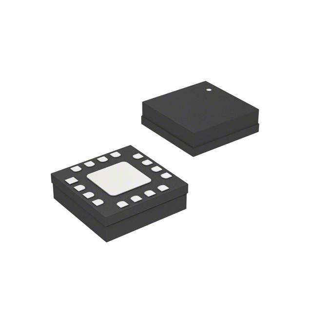
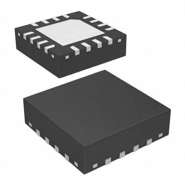
ICGOO电子元器件商城为您提供HMC759LP3E由Hittite设计生产,在icgoo商城现货销售,并且可以通过原厂、代理商等渠道进行代购。 HMC759LP3E价格参考。HittiteHMC759LP3E封装/规格:衰减器, RF Attenuator 0.25dB ~ 31.75dB 10MHz ~ 300MHz 50 Ohms 16-VFQFN Exposed Pad。您可以下载HMC759LP3E参考资料、Datasheet数据手册功能说明书,资料中有HMC759LP3E 详细功能的应用电路图电压和使用方法及教程。
HMC759LP3E 是 Analog Devices Inc.(ADI)生产的一款基于 GaAs(砷化镓)工艺的单刀双掷(SPDT)开关/衰减器集成电路,工作频率范围为 DC 至 18 GHz。该器件具有低插入损耗、高隔离度和出色的线性度特性,因此适用于多种射频和微波通信系统。

 应用场景:
1. 无线通信基础设施
   HMC759LP3E 可用于基站、中继器和其他无线通信设备中,实现信号路径切换或调节信号强度的功能。例如,在多频段基站中,它可以帮助选择不同的频段或调整功率电平以优化信号质量。

2. 测试与测量设备
   在高性能矢量网络分析仪(VNA)、频谱分析仪或信号发生器中,这款器件可以作为信号路径控制的一部分,提供精确的信号衰减或切换功能,从而提高测试精度和灵活性。

3. 雷达系统
   雷达应用需要快速切换和稳定性能的组件,HMC759LP3E 的宽频带和低插损特性使其非常适合用于 X 波段及更高频率的雷达收发模块中,用于信号路由或动态范围扩展。

4. 卫星通信(Satcom)
   卫星地面站或用户终端通常需要处理宽带信号并支持不同增益设置。HMC759LP3E 的高频能力和可靠性使其成为这些系统中的理想选择,可用于上下变频链路中的信号管理。

5. 点对点无线电系统
   在微波回传网络中,这款器件可以用作信号路径控制器,确保在长距离传输时维持稳定的信号质量和数据速率。

6. 军事与航空航天领域
   由于其优异的电气性能和环境适应能力,HMC759LP3E 还被广泛应用于军用通信、电子战系统以及导航设备中,满足严苛条件下的使用需求。

总结来说,HMC759LP3E 凭借其卓越的高频表现和多功能性,能够胜任从商业通信到国防科技的各种复杂应用场景。
| 参数 | 数值 |
| 产品目录 | |
| 描述 | IC ATTENUATOR 0.25DB 16-QFN |
| 产品分类 | |
| 品牌 | Hittite Microwave Corporation |
| 数据手册 | |
| 产品图片 |
|
| 产品型号 | HMC759LP3E |
| rohs | 无铅 / 符合限制有害物质指令(RoHS)规范要求 |
| 产品系列 | - |
| 其它名称 | 1127-1559 |
| 功率(W) | - |
| 容差 | - |
| 封装/外壳 | 16-VFQFN 裸露焊盘 |
| 标准包装 | 100 |
| 衰减值 | 0.25dB ~ 31.75dB |
| 阻抗 | 50 欧姆 |
| 频率范围 | 10MHz ~ 300MHz |


- 商务部:美国ITC正式对集成电路等产品启动337调查
- 曝三星4nm工艺存在良率问题 高通将骁龙8 Gen1或转产台积电
- 太阳诱电将投资9.5亿元在常州建新厂生产MLCC 预计2023年完工
- 英特尔发布欧洲新工厂建设计划 深化IDM 2.0 战略
- 台积电先进制程称霸业界 有大客户加持明年业绩稳了
- 达到5530亿美元!SIA预计今年全球半导体销售额将创下新高
- 英特尔拟将自动驾驶子公司Mobileye上市 估值或超500亿美元
- 三星加码芯片和SET,合并消费电子和移动部门,撤换高东真等 CEO
- 三星电子宣布重大人事变动 还合并消费电子和移动部门
- 海关总署:前11个月进口集成电路产品价值2.52万亿元 增长14.8%


PDF Datasheet 数据手册内容提取
HMC759LP3E v00.0909 0.25 dB LSB BiCMOS MMIC 7-BIT DIGITAL ATTENUATOR, 10 - 300 MHz 8 Typical Applications Features the HMC759LP3e is ideal for: 0.25 dB LsB steps to 31.75 dB t M • Cellular/3G Infrastructure Power-up state selection s • WiBro / WiMAX / 4G High Input IP3: +40 dBm ttL/CMos Compatible, serial Control - • Microwave radio & VsAt L excellent state & step Accuracy ±0.25 dB • test equipment and sensors A single +5V supply t • IF & rF Applications I 16 Lead 3x3mm sMt Package: 9mm2 G I D Functional Diagram General Description - s the HMC759LP3e is a 7-bit BiCMos Digital r Attenuator in a low cost leadless sMt package. this o versatile digital attenuator incorporates off-chip AC t ground capacitors for near DC operation, making it A suitable for a wide variety of rF and IF applications. u the control interface is CMos/ttL compatible and n accepts a three wire serial input. the HMC759LP3e e features user selectable power up states and a serial t t output port for cascading other Hittite serial controlled A components. the HMC759LP3e is housed in a roHs compliant 3x3 mm QFn leadless package, and occupies only 9 mm2. Electrical Specifications T = +25 °C, 50Ω System, with Vdd1 = Vdd2 = +5V & Vctl = 0/+5V A Parameter Frequency (MHz) Min. typ. Max. units Insertion Loss 10 - 300 3.3 4.5 dB Attenuation range 10 - 300 31.75 dB return Loss (rF1, rF2, All Atten. states) 10 - 300 10 dB Attenuation Accuracy: (referenced to Insertion Loss) 10 - 300 ± (0.05 + 1.5% of Atten. settling) Max. dB All Attenuation states 10 - 50 20 dBm Input Power for 1 dB Compression 50 - 300 21 dBm Input third order Intercept Point 10 - 50 39 dBm (two-tone Input Power = 0 dBm each tone) 50 - 300 >40 dBm Bias Current (Idd1 + Idd2) 10 - 300 300 650 1000 µA switching time (50% Le to 90% rF) 10 - 300 15 ns InfoFrmoarti opn rfiucrneis,h edd eblyi vAenarlyog a Dnedvic etos isp blaelcieeve do trod beer asc:c uHraittet iatned Mreliiacbrleo. wHoawvevee r,C noo rpFoorra tpiroicne,, 2d0el iAvelrpyh, aan Rd otoa dpl,a cCeh oerldmerssf:o Arnda,l oMg AD e0v1ic8e2s4, Inc., responsibility is assumed by Analog Devices for its use, nor for any infringements of patents or other One Technology Way, P.O. Box 9106, Norwood, MA 02062-9106 8 - 1 rliicgehntss eo fi sth girrda nptaerdti ebsy t himatp mlicPaayht ioroens nuolret of:rto hm9er 7wits8is ue-s 2eu.n5 dS0epre- ca3infi3yc ap4tiao3tne sn ts ou rb Fjpeaactte xtno:t cr9higa7hnt8gs e-o 2wf Ai5thn0oaulo-t g3n oD3tiec7vei3.c eN s o. OPrhdoneer: O78n1--3li2n9e- 4a7t0 0w (cid:127)w Owrd.ehri totnitlein.ec aot mwww.analog.com Trademarks and registered trademarks aArep thpe lpircopaetrityo onf thSeiur rpesppeoctrivte: oPwhneorsn.e: 978-250-33A4p3p l icoart i oanp Spusp@pohrti:t Ptihteo.nceo: 1m-800-ANALOG-D
HMC759LP3E v00.0909 0.25 dB LSB BiCMOS MMIC 7-BIT DIGITAL ATTENUATOR, 10 - 300 MHz 8 Normalized Attenuation [1] Insertion Loss vs. Temperature [1] (Only Major States are Shown) 0 0 B) t ON LOSS (dB) --21 ++ -284550CCC ATTENUATION (d --11-505 84 d dBB 16 dB L - sM RTI -3 ED -20 A NSE ALIZ -25 t I -4 RM 31.75 dB GI O -30 N I D -5 -35 0 0.05 0.1 0.15 0.2 0.25 0.3 0.35 0.4 0 0.05 0.1 0.15 0.2 0.25 0.3 0.35 0.4 FREQUENCY (GHz) FREQUENCY (GHz) - s r Input Return Loss [1] Output Return Loss [1] o (Only Major States are Shown) (Only Major States are Shown) t A -5 -5 u -10 n B) B) e S (d -15 4 dB S (d -10 0 dB t S S N LO -20 8 dB N LO At R R U U ET -25 ET -15 R 16 dB R -30 31.75 dB 31.75 dB -35 -20 0 0.05 0.1 0.15 0.2 0.25 0.3 0.35 0.4 0 0.05 0.1 0.15 0.2 0.25 0.3 0.35 0.4 FREQUENCY (GHz) FREQUENCY (GHz) Bit Error vs. Frequency [2] Bit Error vs. Attenuation State [2] (Only Major States are Shown) 0.5 0.5 31.75 dB 0.25 0.25 B) B) R (d 300 MHz 200 MHz R (d O O R 0 R 0 R R E E BIT BIT -0.25 -0.25 10 MHz -0.5 -0.5 0 4 8 12 16 20 24 28 32 0 0.05 0.1 0.15 0.2 0.25 0.3 0.35 0.4 ATTENUATION STATE (dB) FREQUENCY (GHz) [1] Data taken with broadband DC blocking on rF input and output ports. [2] C1, C2 = 10nF InfoFrmoarti opn rfiucrneis,h edd eblyi vAenarlyog a Dnedvic etos isp blaelcieeve do trod beer asc:c uHraittet iatned Mreliiacbrleo. wHoawvevee r,C noo rpFoorra tpiroicne,, 2d0el iAvelrpyh, aan Rd otoa dpl,a cCeh oerldmerssf:o Arnda,l oMg AD e0v1ic8e2s4, Inc., responsibility is assumed by Analog Devices for its use, nor for any infringements of patents or other One Technology Way, P.O. Box 9106, Norwood, MA 02062-9106 rights of third parties that mPayh roesnulet f:ro m9 7its8 u-s2e.5 S0pe-c3ifi3ca4tio3n s s u bFjeact xto: c9ha7n8ge- 2wi5th0ou-t 3no3tic7e3. N o OPrhdoneer: O78n1--3li2n9e- 4a7t0 0w (cid:127)w Owrd.ehri totnitlein.ec aot mwww.analog.com 8 - 2 license is granted by implication or otherwise under any patent or patent rights of Analog Devices. Trademarks and registered trademarks aArep thpe lpircopaetrityo onf thSeiur rpesppeoctrivte: oPwhneorsn.e: 978-250-33A4p3p l icoart i oanp Spusp@pohrti:t Ptihteo.nceo: 1m-800-ANALOG-D
HMC759LP3E v00.0909 0.25 dB LSB BiCMOS MMIC 7-BIT DIGITAL ATTENUATOR, 10 - 300 MHz 8 Worst Case Step Error IP3 vs. Attenuation States [1] Between Successive Attenuation States [1] (Only Major States are Shown) 0.2 60 t M 0.15 55 16 dB 0.1 s B) 50 - OR (d 0.05 Bm) 45 8 dB 31.75 dB AL EP ERR -0.050 IP3 (d 40 0 dB t ST 35 -0.1 I G -0.15 30 DI -0.2 31.75 dB 25 0 0.05 0.1 0.15 0.2 0.25 0.3 0.35 0.4 0 0.05 0.1 0.15 0.2 0.25 0.3 0.35 0.4 - FREQUENCY (GHz) FREQUENCY (GHz) s r o Input P1dB vs. Attenuation States [1][2] t (Only Major States are Shown) A 24 u n 8 dB 4 dB e 22 t m) B t d A B ( 20 16 dB d 1 P 18 16 0 0.05 0.1 0.15 0.2 0.25 0.3 0.35 0.4 FREQUENCY (GHz) Serial Control Interface the HMC759LP3e contains a 3-wire sPI compatible digital interface (serIn, CLK, Le). the 7-bit serial word must be loaded MsB first. the positive-edge sensitive CLK and Le requires clean transitions. If mechanical switches are used, sufficient debouncing should be provided. When Le is high, 7-bit data in the serial input register is transferred to the attenuator. When Le is high, CLK is masked to prevent data transition during output loading. [1] C1, C2 = 10nF [2] Part does not enter 1 dB compression at 31.75 dB max attenuation up to 25 dBm input power. InfoFrmoarti opn rfiucrneis,h edd eblyi vAenarlyog a Dnedvic etos isp blaelcieeve do trod beer asc:c uHraittet iatned Mreliiacbrleo. wHoawvevee r,C noo rpFoorra tpiroicne,, 2d0el iAvelrpyh, aan Rd otoa dpl,a cCeh oerldmerssf:o Arnda,l oMg AD e0v1ic8e2s4, Inc., responsibility is assumed by Analog Devices for its use, nor for any infringements of patents or other One Technology Way, P.O. Box 9106, Norwood, MA 02062-9106 8 - 3 rliicgehntss eo fi sth girrda nptaerdti ebsy t himatp mlicPaayht ioroens nuolret of:rto hm9er 7wits8is ue-s 2eu.n5 dS0epre- ca3infi3yc ap4tiao3tne sn ts ou rb Fjpeaactte xtno:t cr9higa7hnt8gs e-o 2wf Ai5thn0oaulo-t g3n oD3tiec7vei3.c eN s o. OPrhdoneer: O78n1--3li2n9e- 4a7t0 0w (cid:127)w Owrd.ehri totnitlein.ec aot mwww.analog.com Trademarks and registered trademarks aArep thpe lpircopaetrityo onf thSeiur rpesppeoctrivte: oPwhneorsn.e: 978-250-33A4p3p l icoart i oanp Spusp@pohrti:t Ptihteo.nceo: 1m-800-ANALOG-D
HMC759LP3E v00.0909 0.25 dB LSB BiCMOS MMIC 7-BIT DIGITAL ATTENUATOR, 10 - 300 MHz 8 Bias Voltage Vdd (V) Idd (typ.) (µA) Parameter typ. t 4.5 580 Min. serial period, tsCK 100 ns M 5.0 650 Control set-up time, t 20 ns Cs s 5.5 710 Control hold-time, t 20 ns CH - Le setup-time, t 10 ns Ln L Control Voltage Table Min. Le pulse width, tLeW 10 ns A Min Le pulse spacing, t 630 ns t Les state Vdd = +5V serial clock hold-time from Le, tCKn 10 ns GI Low 0 to 0.8V @ <1 µA I High 2 to 5V @ <1 µA D - s r o Power-Up States PUP Truth Table t A If Le is set to logic LoW at power-up, the logic state Le PuP1 PuP2 relative Attenuation u of PuP1 and PuP2 determines the power-up state 0 0 0 -31.75 n of the part per PuP truth table. If the Le is kept high 0 1 0 -24 e at power up, power up state will be indeterminate 0 0 1 -16 t therefore is not recommended. 0 1 1 Insertion Loss t A 1 X X Indeterminate Power-On Sequence the ideal power-up sequence is: GnD, Vdd, digital inputs, rF inputs. the relative order of the digital inputs are not important as long as they are powered after Vdd / GnD Truth Table Control Voltage Input reference Insertion Loss D6 D5 D4 D3 D2 D1 D0 (dB) High High High High High High High 0 High High High High High High Low 0.25 High High High High High Low High 0.5 High High High High Low High High 1 High High High Low High High High 2 High High Low High High High High 4 High Low High High High High High 8 Low High High High High High High 16 Low Low Low Low Low Low Low 31.75 Any combination of the above states will provide an attenuation equal to the sum of the bits selected. InfoFrmoarti opn rfiucrneis,h edd eblyi vAenarlyog a Dnedvic etos isp blaelcieeve do trod beer asc:c uHraittet iatned Mreliiacbrleo. wHoawvevee r,C noo rpFoorra tpiroicne,, 2d0el iAvelrpyh, aan Rd otoa dpl,a cCeh oerldmerssf:o Arnda,l oMg AD e0v1ic8e2s4, Inc., responsibility is assumed by Analog Devices for its use, nor for any infringements of patents or other One Technology Way, P.O. Box 9106, Norwood, MA 02062-9106 rights of third parties that mPayh roesnulet f:ro m9 7its8 u-s2e.5 S0pe-c3ifi3ca4tio3n s s u bFjeact xto: c9ha7n8ge- 2wi5th0ou-t 3no3tic7e3. N o OPrhdoneer: O78n1--3li2n9e- 4a7t0 0w (cid:127)w Owrd.ehri totnitlein.ec aot mwww.analog.com 8 - 4 license is granted by implication or otherwise under any patent or patent rights of Analog Devices. Trademarks and registered trademarks aArep thpe lpircopaetrityo onf thSeiur rpesppeoctrivte: oPwhneorsn.e: 978-250-33A4p3p l icoart i oanp Spusp@pohrti:t Ptihteo.nceo: 1m-800-ANALOG-D
HMC759LP3E v00.0909 0.25 dB LSB BiCMOS MMIC 7-BIT DIGITAL ATTENUATOR, 10 - 300 MHz 8 Absolute Maximum Ratings rF Input Power (rF1, rF2) 20 dBm (t = +85 °C) t eLeCtrostAtIC sensItIVe DeVICe M D(sigeirtaIln I nLpeu,t sC LK, PuP1, PuP2) -0.5 to Vdd +0.5V oBserVe HAnDLInG PreCAutIons s Bias Voltage (Vdd) 5.6V - Channel temperature 125 °C L Continuous Pdiss (t = 85 °C) A (derate 9.8 mW/°C above 85 °C) 0.29 W t thermal resistance I 138 °C/W G (channel to ground paddle) I storage temperature -65 to +150 °C D operating temperature -40 to +85 °C - esD sensitivity (HBM) Class 1A s r o t Outline Drawing A u n e t t A notes: 1. LeADFrAMe MAterIAL: CoPPer ALLoY 2. DIMensIons Are In InCHes [MILLIMeters] 3. LeAD sPACInG toLerAnCe Is non-CuMuLAtIVe. 4. PAD Burr LenGtH sHALL Be 0.15mm MAXIMuM. PAD Burr HeIGHt sHALL Be 0.05mm MAXIMuM. 5. PACKAGe WArP sHALL not eXCeeD 0.05mm. 6. ALL GrounD LeADs AnD GrounD PADDLe Must Be soLDereD to PCB rF GrounD. 7. reFer to HIttIte APPLICAtIon note For suGGesteD LAnD PAttern. Package Information Part number Package Body Material Lead Finish MsL rating Package Marking [1] HMC759LP3e roHs-compliant Low stress Injection Molded Plastic 100% matte sn MsL1 [2] 759 XXXX [1] 4-Digit lot number XXXX [2] Max peak reflow temperature of 260 °C InfoFrmoarti opn rfiucrneis,h edd eblyi vAenarlyog a Dnedvic etos isp blaelcieeve do trod beer asc:c uHraittet iatned Mreliiacbrleo. wHoawvevee r,C noo rpFoorra tpiroicne,, 2d0el iAvelrpyh, aan Rd otoa dpl,a cCeh oerldmerssf:o Arnda,l oMg AD e0v1ic8e2s4, Inc., responsibility is assumed by Analog Devices for its use, nor for any infringements of patents or other One Technology Way, P.O. Box 9106, Norwood, MA 02062-9106 8 - 5 rliicgehntss eo fi sth girrda nptaerdti ebsy t himatp mlicPaayht ioroens nuolret of:rto hm9er 7wits8is ue-s 2eu.n5 dS0epre- ca3infi3yc ap4tiao3tne sn ts ou rb Fjpeaactte xtno:t cr9higa7hnt8gs e-o 2wf Ai5thn0oaulo-t g3n oD3tiec7vei3.c eN s o. OPrhdoneer: O78n1--3li2n9e- 4a7t0 0w (cid:127)w Owrd.ehri totnitlein.ec aot mwww.analog.com Trademarks and registered trademarks aArep thpe lpircopaetrityo onf thSeiur rpesppeoctrivte: oPwhneorsn.e: 978-250-33A4p3p l icoart i oanp Spusp@pohrti:t Ptihteo.nceo: 1m-800-ANALOG-D
HMC759LP3E v00.0909 0.25 dB LSB BiCMOS MMIC 7-BIT DIGITAL ATTENUATOR, 10 - 300 MHz 8 Pin Descriptions Pin number Function Description Interface schematic t this pin should be pulled high to M 1 Vdd1 Vdd through a 39 kΩ resistor. s 2 serIn - L 3 Le A t 4 CLK see truth table, Control Voltage table I and timing Diagram. G I 5 PuP1 D - 6 PuP2 s r o t A 7 serout serial input data delayed by 7 clock cycles. u n e t t rF1, this pin is DC coupled and matched to A 8, 13 rF2 50 ohms. Blocking capacitors are required. external capacitors to ground are required. Place 9 - 12 ACG0 - 3 these capacitors close to the package. this pin and package bottom must 14 GnD be connected to rF/DC ground. 15 Vdd2 supply voltage. this pin is not connected internally; however, all data 16 n/C shown herein was measured with this pin connected to rF/DC ground externally. InfoFrmoarti opn rfiucrneis,h edd eblyi vAenarlyog a Dnedvic etos isp blaelcieeve do trod beer asc:c uHraittet iatned Mreliiacbrleo. wHoawvevee r,C noo rpFoorra tpiroicne,, 2d0el iAvelrpyh, aan Rd otoa dpl,a cCeh oerldmerssf:o Arnda,l oMg AD e0v1ic8e2s4, Inc., responsibility is assumed by Analog Devices for its use, nor for any infringements of patents or other One Technology Way, P.O. Box 9106, Norwood, MA 02062-9106 rights of third parties that mPayh roesnulet f:ro m9 7its8 u-s2e.5 S0pe-c3ifi3ca4tio3n s s u bFjeact xto: c9ha7n8ge- 2wi5th0ou-t 3no3tic7e3. N o OPrhdoneer: O78n1--3li2n9e- 4a7t0 0w (cid:127)w Owrd.ehri totnitlein.ec aot mwww.analog.com 8 - 6 license is granted by implication or otherwise under any patent or patent rights of Analog Devices. Trademarks and registered trademarks aArep thpe lpircopaetrityo onf thSeiur rpesppeoctrivte: oPwhneorsn.e: 978-250-33A4p3p l icoart i oanp Spusp@pohrti:t Ptihteo.nceo: 1m-800-ANALOG-D
HMC759LP3E v00.0909 0.25 dB LSB BiCMOS MMIC 7-BIT DIGITAL ATTENUATOR, 10 - 300 MHz 8 Application Circuit t M s - L A t I G I D - s r o t A u n e t t A InfoFrmoarti opn rfiucrneis,h edd eblyi vAenarlyog a Dnedvic etos isp blaelcieeve do trod beer asc:c uHraittet iatned Mreliiacbrleo. wHoawvevee r,C noo rpFoorra tpiroicne,, 2d0el iAvelrpyh, aan Rd otoa dpl,a cCeh oerldmerssf:o Arnda,l oMg AD e0v1ic8e2s4, Inc., responsibility is assumed by Analog Devices for its use, nor for any infringements of patents or other One Technology Way, P.O. Box 9106, Norwood, MA 02062-9106 8 - 7 rliicgehntss eo fi sth girrda nptaerdti ebsy t himatp mlicPaayht ioroens nuolret of:rto hm9er 7wits8is ue-s 2eu.n5 dS0epre- ca3infi3yc ap4tiao3tne sn ts ou rb Fjpeaactte xtno:t cr9higa7hnt8gs e-o 2wf Ai5thn0oaulo-t g3n oD3tiec7vei3.c eN s o. OPrhdoneer: O78n1--3li2n9e- 4a7t0 0w (cid:127)w Owrd.ehri totnitlein.ec aot mwww.analog.com Trademarks and registered trademarks aArep thpe lpircopaetrityo onf thSeiur rpesppeoctrivte: oPwhneorsn.e: 978-250-33A4p3p l icoart i oanp Spusp@pohrti:t Ptihteo.nceo: 1m-800-ANALOG-D
HMC759LP3E v00.0909 0.25 dB LSB BiCMOS MMIC 7-BIT DIGITAL ATTENUATOR, 10 - 300 MHz 8 Evaluation PCB t M s - L A t I G I D - s r o t A u n e t t A List of Materials for Evaluation PCB 125228 [1] the circuit board used in the final application Item Description should use rF circuit design techniques. signal J1, J2 PCB Mount sMA Connector lines should have 50 ohm impedance while the J3 18 Pin DC Connector package ground leads and exposed paddle should J4, J5 DC Pin be connected directly to the ground plane similar C1 - C6 10 nF Capacitor, 0402 Pkg. to that shown. A sufficient number of via holes C7, C8 100 pF Capacitor, 0402 Pkg. should be used to connect the top and bottom C9 1 nF Capacitor, 0402 Pkg. ground planes. the evaluation circuit board shown C10 4.7 µF Capacitor, 0805 Pkg. is available from Hittite upon request. r1 - r4 39K ohm resistor, 0402 Pkg. u1 HMC759LP3e Digital Attenuator PCB [2] 125226 evaluation PCB [1] reference this number when ordering complete evaluation PCB [2] Circuit Board Material: Arlon 25Fr or rogers 4350 InfoFrmoarti opn rfiucrneis,h edd eblyi vAenarlyog a Dnedvic etos isp blaelcieeve do trod beer asc:c uHraittet iatned Mreliiacbrleo. wHoawvevee r,C noo rpFoorra tpiroicne,, 2d0el iAvelrpyh, aan Rd otoa dpl,a cCeh oerldmerssf:o Arnda,l oMg AD e0v1ic8e2s4, Inc., responsibility is assumed by Analog Devices for its use, nor for any infringements of patents or other One Technology Way, P.O. Box 9106, Norwood, MA 02062-9106 rights of third parties that mPayh roesnulet f:ro m9 7its8 u-s2e.5 S0pe-c3ifi3ca4tio3n s s u bFjeact xto: c9ha7n8ge- 2wi5th0ou-t 3no3tic7e3. N o OPrhdoneer: O78n1--3li2n9e- 4a7t0 0w (cid:127)w Owrd.ehri totnitlein.ec aot mwww.analog.com 8 - 8 license is granted by implication or otherwise under any patent or patent rights of Analog Devices. Trademarks and registered trademarks aArep thpe lpircopaetrityo onf thSeiur rpesppeoctrivte: oPwhneorsn.e: 978-250-33A4p3p l icoart i oanp Spusp@pohrti:t Ptihteo.nceo: 1m-800-ANALOG-D