ICGOO在线商城 > 射频/IF 和 RFID > 衰减器 > HMC346LP3E
 Datasheet下载
- 型号: HMC346LP3E
- 制造商: Hittite
- 库位|库存: xxxx|xxxx
- 要求:
| 数量阶梯 | 香港交货 | 国内含税 |
| +xxxx | $xxxx | ¥xxxx |
查看当月历史价格
查看今年历史价格
HMC346LP3E产品简介:
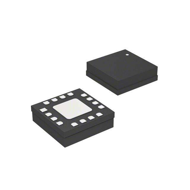
ICGOO电子元器件商城为您提供HMC346LP3E由Hittite设计生产,在icgoo商城现货销售,并且可以通过原厂、代理商等渠道进行代购。 HMC346LP3E价格参考。HittiteHMC346LP3E封装/规格:衰减器, RF Attenuator 0dB ~ 30dB 0Hz ~ 14GHz 50 Ohms 16-VFQFN Exposed Pad。您可以下载HMC346LP3E参考资料、Datasheet数据手册功能说明书,资料中有HMC346LP3E 详细功能的应用电路图电压和使用方法及教程。
HMC346LP3E是Analog Devices Inc.(ADI)推出的一款高性能GaAs MMIC(单片微波集成电路)数字衰减器,广泛应用于射频和微波系统中。该器件工作频率范围为1.5 GHz至3.0 GHz,具备6位数字控制功能,可提供0.5 dB的精细步进调节,最大衰减量达31.5 dB,具有良好的衰减精度和宽带匹配性能。

其主要应用场景包括:

1. 无线通信系统:适用于基站收发信台(BTS)、微波回传链路等,用于信号电平调节,提升链路动态范围与系统稳定性。

2. 雷达系统:在相控阵雷达和电子战(EW)系统中,用于实现波束成形和增益控制,支持快速、精确的信号衰减调整。

3. 测试与测量设备:作为自动测试设备(ATE)中的关键组件,用于校准和调节射频信号强度,确保测试精度。

4. 卫星通信:在地面站和低轨卫星终端中,用于射频前端的功率控制,适应不同链路条件下的信号传输需求。

5. 军用与航空航天电子系统:因其高可靠性与宽温工作能力,适合严苛环境下的射频信号管理。

HMC346LP3E采用紧凑的3 mm × 3 mm SMT封装,便于集成于高密度PCB设计中,同时具备低插入损耗和高输入线性度(IP3),有助于提升系统整体性能。由于其出色的宽带特性和数字控制接口,特别适合需要远程或自动化调节的应用场景。
| 参数 | 数值 |
| 产品目录 | |
| 描述 | IC ATTENUATOR DC-15GHZ 16-QFN |
| 产品分类 | |
| 品牌 | Hittite Microwave Corporation |
| 数据手册 | |
| 产品图片 |
|
| 产品型号 | HMC346LP3E |
| rohs | 无铅 / 符合限制有害物质指令(RoHS)规范要求 |
| 产品系列 | - |
| 其它名称 | 1127-1340 |
| 功率(W) | - |
| 容差 | - |
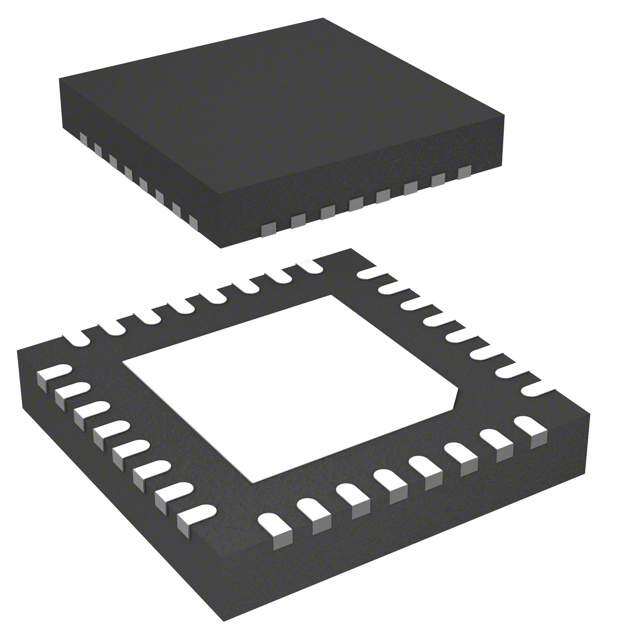
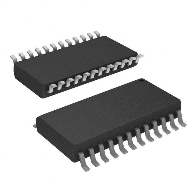
| 封装/外壳 | 16-VFQFN 裸露焊盘 |
| 标准包装 | 100 |
| 衰减值 | 0dB ~ 30dB |
| 阻抗 | 50 欧姆 |
| 频率范围 | 0 ~ 14GHz |


_renders/CS4265-CNZR.jpg)


- 商务部:美国ITC正式对集成电路等产品启动337调查
- 曝三星4nm工艺存在良率问题 高通将骁龙8 Gen1或转产台积电
- 太阳诱电将投资9.5亿元在常州建新厂生产MLCC 预计2023年完工
- 英特尔发布欧洲新工厂建设计划 深化IDM 2.0 战略
- 台积电先进制程称霸业界 有大客户加持明年业绩稳了
- 达到5530亿美元!SIA预计今年全球半导体销售额将创下新高
- 英特尔拟将自动驾驶子公司Mobileye上市 估值或超500亿美元
- 三星加码芯片和SET,合并消费电子和移动部门,撤换高东真等 CEO
- 三星电子宣布重大人事变动 还合并消费电子和移动部门
- 海关总署:前11个月进口集成电路产品价值2.52万亿元 增长14.8%


PDF Datasheet 数据手册内容提取
HMC346LP3 346LP3E / v05.1008 GaAs MMIC VOLTAGE-VARIABLE ATTENUATOR, DC - 14 GHz 5 Typical Applications Features The HMC346LP3 / HMC346LP3E is ideal for: Wide Bandwidth: DC - 14 GHz T M • Basestation Infrastructure Low Phase Shift vs. Attenuation S • Fiber Optics & Broadband Telecom 30 dB Attenuation Range - • Microwave Radio & VSAT Simplifi ed Voltage Control S • Military Radios, Radar, & ECM 3 x 3 x 1 mm SMT Package R O • Test Instrumentation T A Functional Diagram General Description U N The HMC346LP3 & HMC346LP3E are pabsorp- E tive Voltage Variable Attenuators (VVA) in low cost T leadless surface mount plastic packages operating T from DC - 14 GHz. It features an on-chip reference A attenuator for use with an external op-amp to provide simple single voltage attenuation control, 0 to -3V. The device is ideal in designs where an analog DC control signal must control RF signal levels over a 30 dB amplitude range. This VVA is an excellent alterna- tive to the HMC121C8. Electrical Specifi cations, T = +25° C, 50 ohm system A Parameter Min Typical Max Units DC - 10 GHz 1.7 2.2 dB Insertion Loss DC - 14 GHz 2.8 3.3 dB DC - 10 GHz 27 30 dB Attenuation Range DC - 14 GHz 22 27 dB Return Loss DC - 14 GHz 5 10 dB tRISE, tFALL (10/90% RF): 2 ns Switching Characteristics tON, tOFF (50% CTL to 10/90% RF): 8 ns Min. Atten: +8 dBm Input Power for 0.25 dB Compression (0.5 - 8 GHz) Atten. >2 dB: -4 dBm Input Third Order Intercept (0.5 - 8 GHz) Min. Atten: +25 dBm (Two-tone Input Power = -8 dBm Each Tone) Atten. >2 dB: +10 dBm Information furnisheFd obry Apnrailcoge D, edviceelsi vise breylie,v eadn tdo bteo a cpcluaractee a nod rrdelieabrlse., Hpowleevaers, eno coFnotra pcritc eH, idtteiltieve rMy, iacnrdo wtoa pvlaec eC oorrdperosr: aAtnioalnog: Devices, Inc., responsibility is assumed by Analog Devices for its use, nor for any infringements of patents or other One Technology Way, P.O. Box 9106, Norwood, MA 02062-9106 5 - 96 rights of third parties tha2t 0ma yA relpsuhlt faro mR itos uasde. ,S pCechifiecaltmionss fsoubrjedct, toM chAan g0e1 w8ith2ou4t nPotihceo. Nnoe : P9h7o8n-e2: 75801--332394-437 0 0F (cid:127)a Ox:r d9e7r o8n-l2in5e 0at- w33w7w3.analog.com license is granted by implication or otherwise under any patent or patent rights of Analog Devices. Trademarks and registered trademarks are the property of their resOpercdtivee orw Onerns.-line at www.hAiptptilticea.tcioonm Support: Phone: 1-800-ANALOG-D
HMC346LP3 / 346LP3E v05.1008 GaAs MMIC VOLTAGE-VARIABLE ATTENUATOR, DC - 14 GHz 5 Insertion Loss vs. Temperature Relative Attenuation 0 0 T M dB) -1 B) -10 S OSS ( ON (d - N L -2 ATI -20 S O U RTI EN R NSE -3 + -2450 CC ATT -30 O I +85 C T A -4 -40 U 0 2 4 6 8 10 12 14 16 0 2 4 6 8 10 12 14 16 N FREQUENCY (GHz) FREQUENCY (GHz) E T Relative Attenuation vs. T A Return Loss vs. Attenuation Control Voltage @ 10 GHz 0 0 -5 -0.5 V1 c) V2 d dB)-10 E (V -1 OSS (-15 LTAG -1.5 L O RN -20 L V TU RO -2 E-25 T R MIN N -30 5M dABX CO -2.5 -35 -3 0 2 4 6 8 10 12 14 16 0 5 10 15 20 25 30 FREQUENCY (GHz) RELATIVE ATTENUATION (dB) Relative Phase Input IP3 vs. Attenuation* 180 30 5 dB 150 10 dB 25 G) 1250 ddBB E (DE120 23m50a ddxBB Bm) 20 S d E PHA 90 T IP3 ( 15 V U LATI 60 INP 10 E 0 dB R 30 5 3 dB 6 dB 10 dB 0 0 0 2 4 6 8 10 12 14 16 0 2 4 6 8 10 12 14 16 FREQUENCY (GHz) FREQUENCY (GHz) *Two-tone input power = -8 dBm each tone, 1 MHz spacing. Information furnisheFd obry Apnrailcoge D, edviceelsi vise breylie,v eadn tdo bteo a cpcluaractee a nod rrdelieabrlse., Hpowleevaers, eno coFnotra pcritc eH, idtteiltieve rMy, iacnrdo wtoa pvlaec eC oorrdperosr: aAtnioalnog: Devices, Inc., responsibility is assumed by Analog Devices for its use, nor for any infringements of patents or other One Technology Way, P.O. Box 9106, Norwood, MA 02062-9106 rights of third parties tha2t 0ma yA relpsuhlt faro mR itos uasde. ,S pCechifiecaltmionss fsoubrjedct, toM chAan g0e1 w8ith2ou4t nPotihceo. Nnoe : P9h7o8n-e2: 75801--332394-437 0 0F (cid:127)a Ox:r d9e7r o8n-l2in5e 0at- w33w7w3.analog.com 5 - 97 license is granted by implication or otherwise under any patent or patent rights of Analog Devices. Trademarks and registered trademarks are the property of their resOpercdtivee orw Onerns.-line at www.hAiptptilticea.tcioonm Support: Phone: 1-800-ANALOG-D
HMC346LP3 / 346LP3E v05.1008 GaAs MMIC VOLTAGE-VARIABLE ATTENUATOR, DC - 14 GHz 5 Second Harmonic Input IP2 vs. Attenuation* vs. Attenuation, Pin = -8 dBm 70 80 T M 60 70 c) B S d m) 50 C ( 60 S - P2 (dB 40 RMONI 50 OR INPUT I 30 036 dddBBB ECOND HA 40 036 dddBBB T 20 10 dB S 30 10 dB A U 10 20 0 2 4 6 8 10 12 14 16 0 2 4 6 8 10 12 14 16 N FREQUENCY (GHz) FREQUENCY (GHz) E T T A 0.25 dB Compression vs. Attenuation 1 dB Compression vs. Attenuation 15 20 10 15 Bm) m) T 0.25dB (d 05 60 ddBB (REF) UT P1dB (dB 150 U P P N N I I -5 0 0 dB (REF) 6 dB -10 -5 0 2 4 6 8 10 12 14 16 0 2 4 6 8 10 12 14 16 FREQUENCY (GHz) FREQUENCY (GHz) *Two-tone input power = -8 dBm each tone, 1 MHz spacing. Information furnisheFd obry Apnrailcoge D, edviceelsi vise breylie,v eadn tdo bteo a cpcluaractee a nod rrdelieabrlse., Hpowleevaers, eno coFnotra pcritc eH, idtteiltieve rMy, iacnrdo wtoa pvlaec eC oorrdperosr: aAtnioalnog: Devices, Inc., responsibility is assumed by Analog Devices for its use, nor for any infringements of patents or other One Technology Way, P.O. Box 9106, Norwood, MA 02062-9106 5 - 98 rights of third parties tha2t 0ma yA relpsuhlt faro mR itos uasde. ,S pCechifiecaltmionss fsoubrjedct, toM chAan g0e1 w8ith2ou4t nPotihceo. Nnoe : P9h7o8n-e2: 75801--332394-437 0 0F (cid:127)a Ox:r d9e7r o8n-l2in5e 0at- w33w7w3.analog.com license is granted by implication or otherwise under any patent or patent rights of Analog Devices. Trademarks and registered trademarks are the property of their resOpercdtivee orw Onerns.-line at www.hAiptptilticea.tcioonm Support: Phone: 1-800-ANALOG-D
HMC346LP3 / 346LP3E v05.1008 GaAs MMIC VOLTAGE-VARIABLE ATTENUATOR, DC - 14 GHz 5 Absolute Maximum Ratings RF Input Power +18 dBm ELECTROSTATIC SENSITIVE DEVICE T Control Voltage Range +1 to -5V M OBSERVE HANDLING PRECAUTIONS Storage Temperature -65 to +150 °C S Operating Temperature -40 to +85 °C - ESD Sensitivity (HBM) Class 1A S R O T A U N Outline Drawing E T T A NOTES: 1. LEADFRAME MATERIAL: COPPER ALLOY 2. DIMENSIONS ARE IN INCHES [MILLIMETERS] 3. LEAD SPACING TOLERANCE IS NON-CUMULATIVE 4. PAD BURR LENGTH SHALL BE 0.15mm MAXIMUM. PAD BURR HEIGHT SHALL BE 0.05mm MAXIMUM. 5. PACKAGE WARP SHALL NOT EXCEED 0.05mm. 6. ALL GROUND LEADS AND GROUND PADDLE MUST BE SOLDERED TO PCB RF GROUND. 7. REFER TO HITTITE APPLICATION NOTE FOR SUGGESTED LAND PATTERN. Package Information Part Number Package Body Material Lead Finish MSL Rating Package Marking [3] HMC346LP3 Low Stress Injection Molded Plastic Sn/Pb Solder MSL1 [1] 346 XXXX HMC346LP3E RoHS-compliant Low Stress Injection Molded Plastic 100% matte Sn MSL1 [2] 346 XXXX [1] Max peak refl ow temperature of 235 °C [2] Max peak refl ow temperature of 260 °C [3] 4-Digit lot number XXXX Information furnisheFd obry Apnrailcoge D, edviceelsi vise breylie,v eadn tdo bteo a cpcluaractee a nod rrdelieabrlse., Hpowleevaers, eno coFnotra pcritc eH, idtteiltieve rMy, iacnrdo wtoa pvlaec eC oorrdperosr: aAtnioalnog: Devices, Inc., responsibility is assumed by Analog Devices for its use, nor for any infringements of patents or other One Technology Way, P.O. Box 9106, Norwood, MA 02062-9106 rights of third parties tha2t 0ma yA relpsuhlt faro mR itos uasde. ,S pCechifiecaltmionss fsoubrjedct, toM chAan g0e1 w8ith2ou4t nPotihceo. Nnoe : P9h7o8n-e2: 75801--332394-437 0 0F (cid:127)a Ox:r d9e7r o8n-l2in5e 0at- w33w7w3.analog.com 5 - 99 license is granted by implication or otherwise under any patent or patent rights of Analog Devices. Trademarks and registered trademarks are the property of their resOpercdtivee orw Onerns.-line at www.hAiptptilticea.tcioonm Support: Phone: 1-800-ANALOG-D
HMC346LP3 / 346LP3E v05.1008 GaAs MMIC VOLTAGE-VARIABLE ATTENUATOR, DC - 14 GHz 5 Pin Descriptions Pin Number Function Description Interface Schematic T M Package bottom has exposed metal paddle that must also be 1, 3, 7, 10, 12 GND connected to PCB RF ground. S - RF1 This pin is DC coupled and matched to 50 Ohm. Blocking 2, 11 capacitors are required if the RF line potential is not equal to S RF2 0V. R O 4, 9, 13, 14, 15, 16 N/C This pin should be connected to PCB RF ground. T A U N 5, 8 V2, V1 Control input (master). E T T A 6 I Control input (slave). Single-Line Control Driver External op-amp control circuit maintains impedance match while attenuation is varied. Input control ranges from 0 Volts (min. attenuation) to -3.0 Volts (max. attenuation.) Information furnisheFd obry Apnrailcoge D, edviceelsi vise breylie,v eadn tdo bteo a cpcluaractee a nod rrdelieabrlse., Hpowleevaers, eno coFnotra pcritc eH, idtteiltieve rMy, iacnrdo wtoa pvlaec eC oorrdperosr: aAtnioalnog: Devices, Inc., responsibility is assumed by Analog Devices for its use, nor for any infringements of patents or other One Technology Way, P.O. Box 9106, Norwood, MA 02062-9106 5 - 100 rights of third parties tha2t 0ma yA relpsuhlt faro mR itos uasde. ,S pCechifiecaltmionss fsoubrjedct, toM chAan g0e1 w8ith2ou4t nPotihceo. Nnoe : P9h7o8n-e2: 75801--332394-437 0 0F (cid:127)a Ox:r d9e7r o8n-l2in5e 0at- w33w7w3.analog.com license is granted by implication or otherwise under any patent or patent rights of Analog Devices. Trademarks and registered trademarks are the property of their resOpercdtivee orw Onerns.-line at www.hAiptptilticea.tcioonm Support: Phone: 1-800-ANALOG-D
HMC346LP3 / 346LP3E v05.1008 GaAs MMIC VOLTAGE-VARIABLE ATTENUATOR, DC - 14 GHz 5 Evaluation PCB T M S - S R O T A U N E T T A List of Materials for Evaluation PCB 105709 [1] The circuit board used in the fi nal application Item Description should be generated with proper RF circuit design J1 - J2 PCB Mount SMA RF Connector techniques. Signal lines at the RF ports should be J3 - J6 DC Pin 50 ohm impedance and the package ground leads U1 HMC346LP3 / HMC346LP3E VVA and package bottom should be connected directly PCB [2] 105695 Evaluation PCB to the PCB RF ground plane, similar to that shown [1] Reference this number when ordering complete evaluation PCB above. The evaluation circuit board shown above is [2] Circuit Board Material: Rogers 4350 available from Hittite Microwave Corporation upon request. Information furnisheFd obry Apnrailcoge D, edviceelsi vise breylie,v eadn tdo bteo a cpcluaractee a nod rrdelieabrlse., Hpowleevaers, eno coFnotra pcritc eH, idtteiltieve rMy, iacnrdo wtoa pvlaec eC oorrdperosr: aAtnioalnog: Devices, Inc., responsibility is assumed by Analog Devices for its use, nor for any infringements of patents or other One Technology Way, P.O. Box 9106, Norwood, MA 02062-9106 rights of third parties tha2t 0ma yA relpsuhlt faro mR itos uasde. ,S pCechifiecaltmionss fsoubrjedct, toM chAan g0e1 w8ith2ou4t nPotihceo. Nnoe : P9h7o8n-e2: 75801--332394-437 0 0F (cid:127)a Ox:r d9e7r o8n-l2in5e 0at- w33w7w3.analog.com 5 - 101 license is granted by implication or otherwise under any patent or patent rights of Analog Devices. Trademarks and registered trademarks are the property of their resOpercdtivee orw Onerns.-line at www.hAiptptilticea.tcioonm Support: Phone: 1-800-ANALOG-D