ICGOO在线商城 > 射频/IF 和 RFID > 衰减器 > HMC271ALP4E

 Datasheet下载
- 型号: HMC271ALP4E
- 制造商: Hittite
- 库位|库存: xxxx|xxxx
- 要求:
| 数量阶梯 | 香港交货 | 国内含税 |
| +xxxx | $xxxx | ¥xxxx |
查看当月历史价格
查看今年历史价格
HMC271ALP4E产品简介:
ICGOO电子元器件商城为您提供HMC271ALP4E由Hittite设计生产,在icgoo商城现货销售,并且可以通过原厂、代理商等渠道进行代购。 HMC271ALP4E价格参考。HittiteHMC271ALP4E封装/规格:衰减器, RF Attenuator 1dB ~ 31dB 700MHz ~ 3.7GHz 50 Ohms 24-VFQFN Exposed Pad。您可以下载HMC271ALP4E参考资料、Datasheet数据手册功能说明书,资料中有HMC271ALP4E 详细功能的应用电路图电压和使用方法及教程。
HMC271ALP4E 是由 Analog Devices Inc.(ADI)公司生产的一款数字衰减器,属于射频(RF)和微波器件类别。该器件广泛应用于需要精确控制射频信号强度的场合。

主要应用场景包括:

1. 通信系统:在无线基站、微波通信系统中用于调节发射或接收信号的强度,实现自动增益控制(AGC),确保信号在不同距离和环境下保持稳定。

2. 测试与测量设备:用于信号源或频谱分析仪等测试仪器中,提供精确可调的信号衰减,以满足不同测试需求。

3. 雷达系统:在雷达接收链路中调节信号电平,防止接收机过载,同时提高系统的动态范围和灵敏度。

4. 工业控制系统:在工业无线通信或远程监控系统中,用于优化射频信号传输,提高系统稳定性和可靠性。

5. 航空航天与国防:在军用通信、电子战系统中用于信号调节和干扰抑制。

HMC271ALP4E 支持 0.1 至 2.7 GHz 频率范围,具备 6 位数字控制,衰减范围达 31.5 dB,具有高精度、低插入损耗和快速响应等优点,适用于高性能射频系统设计。
| 参数 | 数值 |
| 产品目录 | |
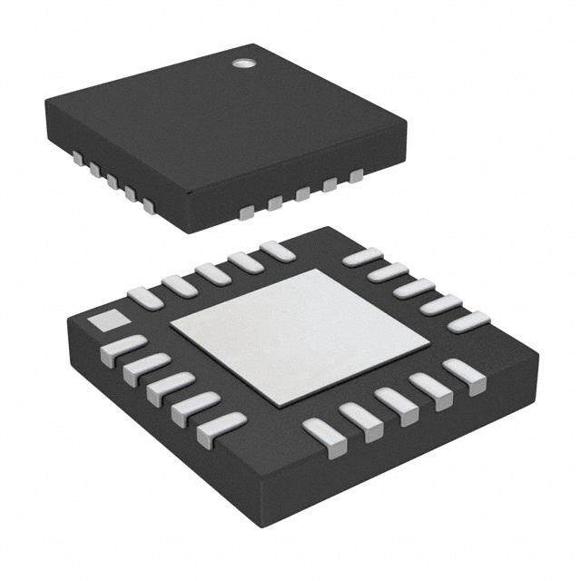
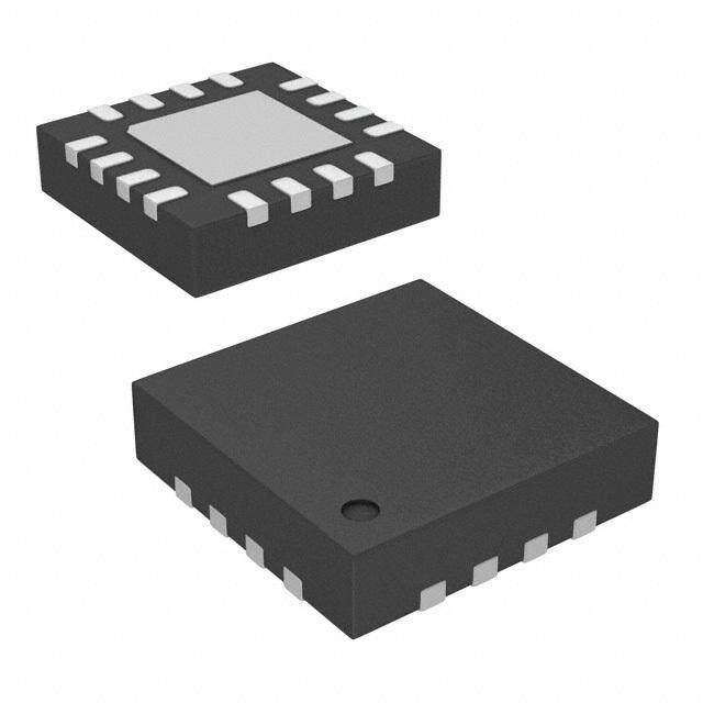
| 描述 | IC ATTENUATOR 5BIT 1DB 24-QFN |
| 产品分类 | |
| 品牌 | Hittite Microwave Corporation |
| 数据手册 | |
| 产品图片 |
|
| 产品型号 | HMC271ALP4E |
| rohs | 无铅 / 符合限制有害物质指令(RoHS)规范要求 |
| 产品系列 | - |
| 其它名称 | 1127-1312 |
| 功率(W) | - |
| 容差 | - |
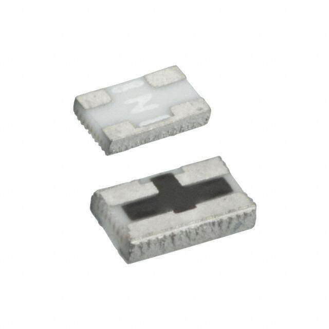
| 封装/外壳 | 24-VFQFN 裸露焊盘 |
| 标准包装 | 100 |
| 衰减值 | 1dB ~ 31dB |
| 阻抗 | 50 欧姆 |
| 频率范围 | 700MHz ~ 3.7GHz |


- 商务部:美国ITC正式对集成电路等产品启动337调查
- 曝三星4nm工艺存在良率问题 高通将骁龙8 Gen1或转产台积电
- 太阳诱电将投资9.5亿元在常州建新厂生产MLCC 预计2023年完工
- 英特尔发布欧洲新工厂建设计划 深化IDM 2.0 战略
- 台积电先进制程称霸业界 有大客户加持明年业绩稳了
- 达到5530亿美元!SIA预计今年全球半导体销售额将创下新高
- 英特尔拟将自动驾驶子公司Mobileye上市 估值或超500亿美元
- 三星加码芯片和SET,合并消费电子和移动部门,撤换高东真等 CEO
- 三星电子宣布重大人事变动 还合并消费电子和移动部门
- 海关总署:前11个月进口集成电路产品价值2.52万亿元 增长14.8%


PDF Datasheet 数据手册内容提取
HMC271ALP4 / 271ALP4E v02.0311 1 dB LSB GaAs MMIC 5-BIT SERIAL CONTROL DIGITAL ATTENUATOR, 0.7 - 3.7 GHz 8 Typical Applications Features the HMC271ALP4(e) is ideal for: 1 dB LsB steps to 31 dB t M • Cellular/3G Infrastructure CMos Compatible serial Data Interface s • Fixed Wireless, WiMax & WiBro sPI Compatible serial output E - • test Instrumentation ±0.4 dB typical Bit error L A 24 Lead 4x4mm QFn Package: 16mm² t Included in the HMC-DK0T04 Designer’s Kit I G DI Functional Diagram General Description E - the HMC271ALP4(e) is a broadband 5-bit positive s control GaAs IC digital attenuator with CMos com- r patible serial-to-parallel drivers in a low cost lead- o L less QFn 4x4 mm sMt package. Covering 0.7 to t 3.7 GHz, the insertion loss is typically less than 2.5 A u dB. the attenuator bit values are 1 (LsB), 2, 4, 8, O n and 16 dB for a total attenuation of 31 dB. Accuracy e is excellent at ± 0.4 dB typical with an IIP3 of up to t +48 dBm. Five bit CMos compatible serial control t words are used to select each attenuation state. A A S single Vcc bias of +3V to +5V applied through an external 5 kohm resistor is required. B Electrical Specifications, T = +25° C, Vcc = +3V to +5V A O Parameter Frequency Min. typical Max. units 0.7 - 1.4 GHz 1.9 2.4 dB 1.4 - 2.3 GHz 2.3 2.8 dB Insertion Loss 2.3 - 2.7 GHz 2.6 3.1 dB 2.7 - 3.7 GHz 2.8 3.3 dB Attenuation range 0.7 - 3.7 GHz 31 dB 0.7 - 1.4 GHz 12 dB return Loss (rF1 & rF2, All Atten. states) 1.4 - 2.7 GHz 15 dB 2.7 - 3.7 GHz 16 dB Attenuation Accuracy: (referenced to Insertion Loss) All Attenuation states 0.7 - 0.9 GHz ± (0.4 + 5% of Atten. setting) Max dB 0.9 - 2.2 GHz ± (0.4 + 4% of Atten. setting) Max dB 2.2 - 3.7 GHz ± (0.4 + 6% of Atten. setting) Max dB Vcc = 5V 24 dBm Input Power for 0.1 dB Compression 0.7 - 3.7 GHz Vcc = 3V 22 dBm Input third order Intercept Point Vcc = 5V 48 dBm 0.7 - 3.7 GHz (two-tone Input Power = 0 dBm each tone) Vcc = 3V 46 dBm switching Characteristics trIse, tFALL (10/90% rF) 750 ns 0.7 - 3.7 GHz ton, toFF (Latch enable to 10/90% rF) 830 ns InforFmaotiro np fruircniseh,e dd beyl iAvnealroyg Daenvidce st ois pbelaliecveed otor dbee arcsc:u rHateit taintde reMliaibcler. oHwowaevveer, Cnoo rpFoorr aptriiocen,, d2e0liv Aerlyp, haand R too apdla,c Ce horedlemrss: fAonrdal,o gM DAe v0ic1e8s2, 4Inc., responsibility is assumed by Analog Devices for its use, nor for any infringements of patents or other One Technology Way, P.O. Box 9106, Norwood, MA 02062-9106 8 - 1 rliicgehntss eo fi sth girrda nptaerdti ebsy t himatp mlicaaPyt iorhenso uonlrt ofertoh:m e9r wit7sis 8ues -eu2.n dS5ep0re ca-inf3iyc 3aptia4otne3sn ts ou rb jpeFacttae tnoxt c:r hig9ahn7tgs 8eo wf- 2Aithn5oau0lot g-n 3oDti3ecve7i.c 3eNso . POhrodnee:r 7 O81n-3-l2i9n-e4 7a0t0 w(cid:127) wOrwde.hr oitntliitnee. cato wmww.analog.com Trademarks and registered trademarks arAe tphep plriocpearttyi oof nth eSir urepsppecotivret :o wPnehrso.ne: 978-250-3A3p4p3li c aotrio na Spuppsp@orht: iPtthitoen.ec: o1-m800-ANALOG-D
HMC271ALP4 / 271ALP4E v02.0311 1 dB LSB GaAs MMIC 5-BIT SERIAL CONTROL DIGITAL ATTENUATOR, 0.7 - 3.7 GHz 8 Return Loss RF1, RF2 Insertion Loss (Only Major States are Shown) 0 0 t -0.5 +25C -5 M dB) -1 +-4805CC B) 16 dB 4 dB 8 dB 31 dB s SS (-1.5 S (d-10 E O S - ON L -2 N LO-15 L INSERTI-2-.53 RETUR-20 2 dB T ItA G -25 -3.5 1 dB I.L. I D -4 -30 0.5 1 1.5 2 2.5 3 3.5 4 0.5 1 E1.5 2 2.5 3 3.5 4 - FREQUENCY (GHz) FREQUENCY (GHz) s r Normalized Attenuation Bit LError o (Only Major States are Shown) vs. Attenuation State t A 0 2 u B) O N (d -5 1.5 n UATIO -10 dB) 1 0.9 GHz 1.9 GHz 2.4 GHz te TEN -15 OR ( t AT S RR 0.5 A D -20 E E T ALIZ -25 BI 0 M R -0.5 NO -30 B 3.5 GHz -35 -1 0.5 1 1.5 2 2.5 3 3.5 4 0 4 8 12 16 20 24 28 32 FREQUENCY (GHz) ATTENUATION STATE (dB) O Bit Error vs. Frequency Relative Phase vs. Frequency (Only Major States are Shown) (Only Major States are Shown) 4 100 75 3 eg.) 50 R (dB) 2 16 dB 8 dB 1, 2, 4 dB ASE (d 25 31 dB 16 dB O H R P 0 BIT ER 1 31 dB ATIVE -25 L RE -50 0 1, 2, 4, 8 dB -75 -1 -100 0.5 1 1.5 2 2.5 3 3.5 4 0 0.5 1 1.5 2 2.5 3 3.5 4 FREQUENCY (GHz) FREQUENCY (GHz) Note: All Data Typical Over Voltage (+3V to +5V) & Temperature (-40°C to +85°C). InforFmaotiro np fruircniseh,e dd beyl iAvnealroyg Daenvidce st ois pbelaliecveed otor dbee arcsc:u rHateit taintde reMliaibcler. oHwowaevveer, Cnoo rpFoorr aptriiocen,, d2e0liv Aerlyp, haand R too apdla,c Ce horedlemrss: fAonrdal,o gM DAe v0ic1e8s2, 4Inc., responsibility is assumed by Analog Devices for its use, nor for any infringements of patents or other One Technology Way, P.O. Box 9106, Norwood, MA 02062-9106 rights of third parties that maPy rhesounlt fero:m 9 it7s 8us-e2. S5p0ec-if3ic3ati4on3s s u b jeFcta tox c: h9an7g8e w-2ith5ou0t -n3oti3ce7. 3No POhrodnee:r 7 O81n-3-l2i9n-e4 7a0t0 w(cid:127) wOrwde.hr oitntliitnee. cato wmww.analog.com 8 - 2 license is granted by implication or otherwise under any patent or patent rights of Analog Devices. Trademarks and registered trademarks arAe tphep plriocpearttyi oof nth eSir urepsppecotivret :o wPnehrso.ne: 978-250-3A3p4p3li c aotrio na Spuppsp@orht: iPtthitoen.ec: o1-m800-ANALOG-D
HMC271ALP4 / 271ALP4E v02.0311 1 dB LSB GaAs MMIC 5-BIT SERIAL CONTROL DIGITAL ATTENUATOR, 0.7 - 3.7 GHz 8 Worst Case Step Error Between Successive Attenuation States Digital Control Voltages 1.2 state Vcc = +5V Vcc = +3V t M 0.8 Low 0 to 1.3V 0 to 0.7V High 3.5 to 5V 2.3 to 3V s B) d 0.4 - OR ( Serial Input Truth Table E L RR 0 E tA STEP -0.4 eLnaatcbhle Cslhoicftk reset Function T I X X L shift register cleared G -0.8 X á H shift register clocked I D -1.2 Contents of shift register 0.5 1 1.5 2 2.5 3 3.5 4 á XE H transferred to Digital - FREQUENCY (GHz) Attenuator s r Timing Truth Table o L t symbol Vcc = +5V Vcc = +3V units serial Data Input Attenuation A Parameter setting u Min. Max. Min. Max. C1 C2 C4 C8 C16 rF1 - rF2 O n serial Input setup reference ts 20 - 100 - ns High High High High High time I.L. e t Hold time from serial th 0 - 5 - ns Low High High High High 1 dB Input to shift Clock t High Low High High High 2 dB A setup time from S High High Low High High 4 dB shift Clock to Latch tlsup 40 - 100 - ns enable High High High Low High 8 dB Propagation delay, High High High High Low 16 dB Latch enable to C1 tpd - 30 - 70 ns B 31 dB through C16 Low Low Low Low Low Max. Atten. setup time from - 20 - 50 - ns Any combination of the above states will provide an attenuation reset to shift Clock approximately equal to the sum of the bits selected. Clock Frequency fOclk - 30 - 10 MHz (1/tclk) Timing Diagram InforFmaotiro np fruircniseh,e dd beyl iAvnealroyg Daenvidce st ois pbelaliecveed otor dbee arcsc:u rHateit taintde reMliaibcler. oHwowaevveer, Cnoo rpFoorr aptriiocen,, d2e0liv Aerlyp, haand R too apdla,c Ce horedlemrss: fAonrdal,o gM DAe v0ic1e8s2, 4Inc., responsibility is assumed by Analog Devices for its use, nor for any infringements of patents or other One Technology Way, P.O. Box 9106, Norwood, MA 02062-9106 8 - 3 rliicgehntss eo fi sth girrda nptaerdti ebsy t himatp mlicaaPyt iorhenso uonlrt ofertoh:m e9r wit7sis 8ues -eu2.n dS5ep0re ca-inf3iyc 3aptia4otne3sn ts ou rb jpeFacttae tnoxt c:r hig9ahn7tgs 8eo wf- 2Aithn5oau0lot g-n 3oDti3ecve7i.c 3eNso . POhrodnee:r 7 O81n-3-l2i9n-e4 7a0t0 w(cid:127) wOrwde.hr oitntliitnee. cato wmww.analog.com Trademarks and registered trademarks arAe tphep plriocpearttyi oof nth eSir urepsppecotivret :o wPnehrso.ne: 978-250-3A3p4p3li c aotrio na Spuppsp@orht: iPtthitoen.ec: o1-m800-ANALOG-D
HMC271ALP4 / 271ALP4E v02.0311 1 dB LSB GaAs MMIC 5-BIT SERIAL CONTROL DIGITAL ATTENUATOR, 0.7 - 3.7 GHz 8 Logic / Functional Diagram t M s E - L A t T I G I D E - s r L o t A u O n e t t S A Programming Example to Select 1 dB Attenuation State B O InforFmaotiro np fruircniseh,e dd beyl iAvnealroyg Daenvidce st ois pbelaliecveed otor dbee arcsc:u rHateit taintde reMliaibcler. oHwowaevveer, Cnoo rpFoorr aptriiocen,, d2e0liv Aerlyp, haand R too apdla,c Ce horedlemrss: fAonrdal,o gM DAe v0ic1e8s2, 4Inc., responsibility is assumed by Analog Devices for its use, nor for any infringements of patents or other One Technology Way, P.O. Box 9106, Norwood, MA 02062-9106 rights of third parties that maPy rhesounlt fero:m 9 it7s 8us-e2. S5p0ec-if3ic3ati4on3s s u b jeFcta tox c: h9an7g8e w-2ith5ou0t -n3oti3ce7. 3No POhrodnee:r 7 O81n-3-l2i9n-e4 7a0t0 w(cid:127) wOrwde.hr oitntliitnee. cato wmww.analog.com 8 - 4 license is granted by implication or otherwise under any patent or patent rights of Analog Devices. Trademarks and registered trademarks arAe tphep plriocpearttyi oof nth eSir urepsppecotivret :o wPnehrso.ne: 978-250-3A3p4p3li c aotrio na Spuppsp@orht: iPtthitoen.ec: o1-m800-ANALOG-D
HMC271ALP4 / 271ALP4E v02.0311 1 dB LSB GaAs MMIC 5-BIT SERIAL CONTROL DIGITAL ATTENUATOR, 0.7 - 3.7 GHz 8 Pin Descriptions t Pin number Function Description Interface schematic M these pins are not connected internally. However, all data 1, 3, 4, 6, 10, 12, 13, s n/C shown herein was measured with these pins connected 15, 16, 18 to rF/DC Ground. E - L this pin is DC coupled and matched to 50 ohms A 2, 17 rF1, rF2 Blocking capacitors are required. select value based on t lowest frequency of operation. T I G I D E - s serial data output. serial input data 5 serial output r delayed by 8 clock cycles. o L t A u O n e t t A 7 reset S B see truth table, control voltage table and timing diagram. 8 shift Clock O 9 Latch enable 11 serial Input 14 Vcc supply Voltage. Package bottom has an exposed metal paddle that must also 19 - 24 GnD be connected to rF/DC Ground. InforFmaotiro np fruircniseh,e dd beyl iAvnealroyg Daenvidce st ois pbelaliecveed otor dbee arcsc:u rHateit taintde reMliaibcler. oHwowaevveer, Cnoo rpFoorr aptriiocen,, d2e0liv Aerlyp, haand R too apdla,c Ce horedlemrss: fAonrdal,o gM DAe v0ic1e8s2, 4Inc., responsibility is assumed by Analog Devices for its use, nor for any infringements of patents or other One Technology Way, P.O. Box 9106, Norwood, MA 02062-9106 8 - 5 rliicgehntss eo fi sth girrda nptaerdti ebsy t himatp mlicaaPyt iorhenso uonlrt ofertoh:m e9r wit7sis 8ues -eu2.n dS5ep0re ca-inf3iyc 3aptia4otne3sn ts ou rb jpeFacttae tnoxt c:r hig9ahn7tgs 8eo wf- 2Aithn5oau0lot g-n 3oDti3ecve7i.c 3eNso . POhrodnee:r 7 O81n-3-l2i9n-e4 7a0t0 w(cid:127) wOrwde.hr oitntliitnee. cato wmww.analog.com Trademarks and registered trademarks arAe tphep plriocpearttyi oof nth eSir urepsppecotivret :o wPnehrso.ne: 978-250-3A3p4p3li c aotrio na Spuppsp@orht: iPtthitoen.ec: o1-m800-ANALOG-D
HMC271ALP4 / 271ALP4E v02.0311 1 dB LSB GaAs MMIC 5-BIT SERIAL CONTROL DIGITAL ATTENUATOR, 0.7 - 3.7 GHz 8 Application Circuit t M s E - L A t T I G I D E - s r L o t A u O n e t t S A B O DC blocking capacitors C1 & C2 are required on RF1 & RF2. Choose C1 = C2 = 100 ~ 300 pF to allow lowest customer specific frequency to pass with minimal loss. R1 = 5 kOhm is required to supply voltage to the circuit through either PIN 2 or PIN 17. InforFmaotiro np fruircniseh,e dd beyl iAvnealroyg Daenvidce st ois pbelaliecveed otor dbee arcsc:u rHateit taintde reMliaibcler. oHwowaevveer, Cnoo rpFoorr aptriiocen,, d2e0liv Aerlyp, haand R too apdla,c Ce horedlemrss: fAonrdal,o gM DAe v0ic1e8s2, 4Inc., responsibility is assumed by Analog Devices for its use, nor for any infringements of patents or other One Technology Way, P.O. Box 9106, Norwood, MA 02062-9106 rights of third parties that maPy rhesounlt fero:m 9 it7s 8us-e2. S5p0ec-if3ic3ati4on3s s u b jeFcta tox c: h9an7g8e w-2ith5ou0t -n3oti3ce7. 3No POhrodnee:r 7 O81n-3-l2i9n-e4 7a0t0 w(cid:127) wOrwde.hr oitntliitnee. cato wmww.analog.com 8 - 6 license is granted by implication or otherwise under any patent or patent rights of Analog Devices. Trademarks and registered trademarks arAe tphep plriocpearttyi oof nth eSir urepsppecotivret :o wPnehrso.ne: 978-250-3A3p4p3li c aotrio na Spuppsp@orht: iPtthitoen.ec: o1-m800-ANALOG-D
HMC271ALP4 / 271ALP4E v02.0311 1 dB LSB GaAs MMIC 5-BIT SERIAL CONTROL DIGITAL ATTENUATOR, 0.7 - 3.7 GHz 8 Absolute Maximum Ratings Digital Inputs (reset, shift Clock, t Latch enable & serial Input) -0.5 to (Vcc + 0.5) V eLeCtrostAtIC sensItIVe DeVICe M oBserVe HAnDLInG PreCAutIons Digital outputs (serial output) -0.5 to (Vcc + 0.5) V s DC Current on serial output ±35 mA E - Bias Voltage (Vcc) +5.6 V L A storage temperature -65 to +150 °C t operating temperature -40 to +85 °C T I G rF Input Power (0.7 - 3.7 GHz) +26 dBm I D esD sensitivity (HBM) Class 1A E - s r Outline Drawing o L t A u O n e t t A S B O notes: 1. LeADFrAMe MAterIAL: CoPPer ALLoY 2. DIMensIons Are In InCHes [MILLIMeters] 3. LeAD sPACInG toLerAnCe Is non-CuMuLAtIVe 4. PAD Burr LenGtH sHALL Be 0.15mm MAXIMuM. PAD Burr HeIGHt sHALL Be 0.05mm MAXIMuM. 5. PACKAGe WArP sHALL not eXCeeD 0.05mm. 6. ALL GrounD LeADs AnD GrounD PADDLe Must Be soLDereD to PCB rF GrounD. 7. reFer to HIttIte APPLICAtIon note For suGGesteD LAnD PAttern. Package Information Part number Package Body Material Lead Finish MsL rating Package Marking [3] HMC271ALP4 Low stress Injection Molded Plastic sn/Pb solder MsL1 [1] H271A XXXX HMC271ALP4e roHs-compliant Low stress Injection Molded Plastic 100% matte sn MsL1 [2] H271A XXXX [1] Max peak reflow temperature of 235 °C [2] Max peak reflow temperature of 260 °C [3] 4-Digit lot number XXXX InforFmaotiro np fruircniseh,e dd beyl iAvnealroyg Daenvidce st ois pbelaliecveed otor dbee arcsc:u rHateit taintde reMliaibcler. oHwowaevveer, Cnoo rpFoorr aptriiocen,, d2e0liv Aerlyp, haand R too apdla,c Ce horedlemrss: fAonrdal,o gM DAe v0ic1e8s2, 4Inc., responsibility is assumed by Analog Devices for its use, nor for any infringements of patents or other One Technology Way, P.O. Box 9106, Norwood, MA 02062-9106 8 - 7 rliicgehntss eo fi sth girrda nptaerdti ebsy t himatp mlicaaPyt iorhenso uonlrt ofertoh:m e9r wit7sis 8ues -eu2.n dS5ep0re ca-inf3iyc 3aptia4otne3sn ts ou rb jpeFacttae tnoxt c:r hig9ahn7tgs 8eo wf- 2Aithn5oau0lot g-n 3oDti3ecve7i.c 3eNso . POhrodnee:r 7 O81n-3-l2i9n-e4 7a0t0 w(cid:127) wOrwde.hr oitntliitnee. cato wmww.analog.com Trademarks and registered trademarks arAe tphep plriocpearttyi oof nth eSir urepsppecotivret :o wPnehrso.ne: 978-250-3A3p4p3li c aotrio na Spuppsp@orht: iPtthitoen.ec: o1-m800-ANALOG-D
HMC271ALP4 / 271ALP4E v02.0311 1 dB LSB GaAs MMIC 5-BIT SERIAL CONTROL DIGITAL ATTENUATOR, 0.7 - 3.7 GHz 8 Evaluation Circuit Board t M s E - L A t T I G I D E - s r L o t A u O n e t t S A B O List of Materials for Evaluation PCB 108782 [1] the circuit board used in the application should Item Description use rF circuit design techniques. signal lines sho- J1 - J2 PCB Mount sMA Connector uld have 50 ohm impedance while the package J3 18 Pin DC Connector ground leads and exposed ground paddle should J6, J7 DC Pin be connected directly to the ground plane similar to C1, C2 100 pF Capacitor, 0402 Pkg. that shown below. A sufficient number of via holes C3 0.01 µF Capacitor, 0402 Pkg. should be used to connect the top and bottom r1 5 kohm resistor, 0402 Pkg. ground planes. the evaluation circuit board as u1 HMC271ALP4(e) Digital Attenuator shown is available from Hittite Microwave Corpora- PCB [2] 108780 evaluation PCB tion upon request. [1] reference this number when ordering complete evaluation PCB [2] Circuit Board Material: rogers 4350 InforFmaotiro np fruircniseh,e dd beyl iAvnealroyg Daenvidce st ois pbelaliecveed otor dbee arcsc:u rHateit taintde reMliaibcler. oHwowaevveer, Cnoo rpFoorr aptriiocen,, d2e0liv Aerlyp, haand R too apdla,c Ce horedlemrss: fAonrdal,o gM DAe v0ic1e8s2, 4Inc., responsibility is assumed by Analog Devices for its use, nor for any infringements of patents or other One Technology Way, P.O. Box 9106, Norwood, MA 02062-9106 rights of third parties that maPy rhesounlt fero:m 9 it7s 8us-e2. S5p0ec-if3ic3ati4on3s s u b jeFcta tox c: h9an7g8e w-2ith5ou0t -n3oti3ce7. 3No POhrodnee:r 7 O81n-3-l2i9n-e4 7a0t0 w(cid:127) wOrwde.hr oitntliitnee. cato wmww.analog.com 8 - 8 license is granted by implication or otherwise under any patent or patent rights of Analog Devices. Trademarks and registered trademarks arAe tphep plriocpearttyi oof nth eSir urepsppecotivret :o wPnehrso.ne: 978-250-3A3p4p3li c aotrio na Spuppsp@orht: iPtthitoen.ec: o1-m800-ANALOG-D