ICGOO在线商城 > 隔离器 > 光隔离器 - 逻辑输出 > PC410L0NIP0F

 Datasheet下载
- 型号: PC410L0NIP0F
- 制造商: Sharp Microelectronics
- 库位|库存: xxxx|xxxx
- 要求:
| 数量阶梯 | 香港交货 | 国内含税 |
| +xxxx | $xxxx | ¥xxxx |
查看当月历史价格
查看今年历史价格
PC410L0NIP0F产品简介:
ICGOO电子元器件商城为您提供PC410L0NIP0F由Sharp Microelectronics设计生产,在icgoo商城现货销售,并且可以通过原厂、代理商等渠道进行代购。 PC410L0NIP0F价格参考。Sharp MicroelectronicsPC410L0NIP0F封装/规格:光隔离器 - 逻辑输出, Logic Output Optoisolator 10Mbps Open Collector 3750Vrms 1 Channel 10kV/µs CMTI 5-SOP。您可以下载PC410L0NIP0F参考资料、Datasheet数据手册功能说明书,资料中有PC410L0NIP0F 详细功能的应用电路图电压和使用方法及教程。
PC410L0NIP0F是由Sharp Microelectronics(现为OmniVision旗下品牌)生产的一款光隔离器(光电耦合器),属于逻辑输出型光耦。该器件主要用于实现输入与输出之间的电气隔离,广泛应用于需要抗干扰和安全隔离的电子系统中。

典型应用场景包括:工业自动化控制设备中的信号隔离,如PLC(可编程逻辑控制器)、I/O模块等;开关电源中的反馈控制电路,用于隔离高压侧与低压控制侧,提升系统安全性;通信设备中防止地环路干扰;以及医疗电子设备中满足安全隔离标准。此外,也常用于电机驱动器、逆变器和电池管理系统中,确保控制信号可靠传输的同时避免高压对低压电路的损害。

PC410L0NIP0F具有高隔离电压、低功耗、快速响应和高可靠性等特点,适合在噪声大或电压波动的环境中稳定工作。其逻辑输出结构可直接与数字电路(如微处理器、FPGA、逻辑门)接口,简化设计。由于采用紧凑的表面贴装封装,适用于空间受限的高密度电路板设计。

综上,该光耦适用于各类需电气隔离的工业、电源、通信及消费类电子系统,是保障电路安全与信号完整性的重要元件。
| 参数 | 数值 |
| 产品目录 | |
| 描述 | PHOTOCOUPLER OPIC 5-SOP |
| 产品分类 | |
| 品牌 | Sharp Microelectronics |
| 数据手册 | http://www.sharpsma.com/webfm_send/1114 |
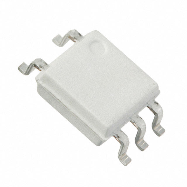
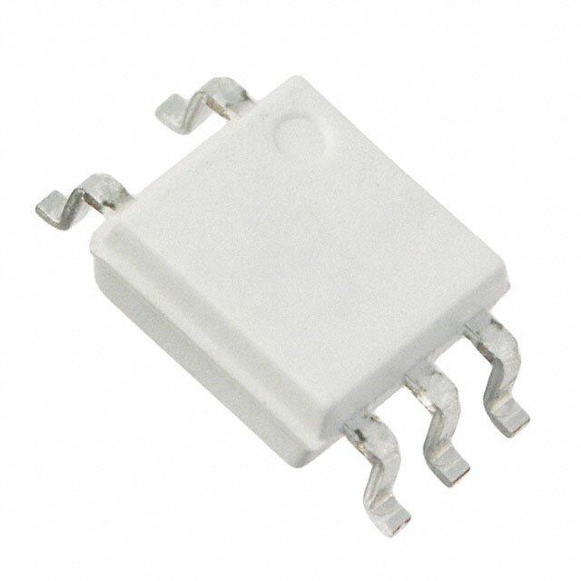
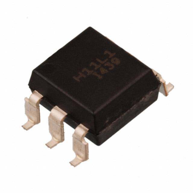
| 产品图片 |
|
| 产品型号 | PC410L0NIP0F |
| rohs | 无铅 / 符合限制有害物质指令(RoHS)规范要求 |
| 产品系列 | OPIC™ |
| 上升/下降时间(典型值) | 20ns, 10ns |
| 产品目录页面 | |
| 传播延迟tpLH/tpHL(最大值) | 75ns, 75ns |
| 供应商器件封装 | 5-SOP |
| 共模瞬态抗扰度(最小值) | 10kV/µs |
| 其它名称 | 425-2141-1 |
| 包装 | 剪切带 (CT) |
| 安装类型 | 表面贴装 |
| 封装/外壳 | 6-SOIC(0.173",4.40mm 宽,5 引线) |
| 工作温度 | -40°C ~ 85°C |
| 数据速率 | 10Mbps |
| 标准包装 | 1 |
| 电压-正向(Vf)(典型值) | 1.6V |
| 电压-电源 | 4.5 V ~ 5.5 V |
| 电压-隔离 | 3750Vrms |
| 电流-DC正向(If) | 20mA |
| 电流-输出/通道 | 50mA |
| 输入-输入侧1/输入侧2 | 1/0 |
| 输入类型 | DC |
| 输出类型 | 开路集电极 |
| 通道数 | 1 |


- 商务部:美国ITC正式对集成电路等产品启动337调查
- 曝三星4nm工艺存在良率问题 高通将骁龙8 Gen1或转产台积电
- 太阳诱电将投资9.5亿元在常州建新厂生产MLCC 预计2023年完工
- 英特尔发布欧洲新工厂建设计划 深化IDM 2.0 战略
- 台积电先进制程称霸业界 有大客户加持明年业绩稳了
- 达到5530亿美元!SIA预计今年全球半导体销售额将创下新高
- 英特尔拟将自动驾驶子公司Mobileye上市 估值或超500亿美元
- 三星加码芯片和SET,合并消费电子和移动部门,撤换高东真等 CEO
- 三星电子宣布重大人事变动 还合并消费电子和移动部门
- 海关总署:前11个月进口集成电路产品价值2.52万亿元 增长14.8%


PDF Datasheet 数据手册内容提取
PC410L0NIP0F Series PC410L0NIP0F High Speed 10Mb/s, High CMR Mini-flat Package ∗OPIC Series Photocoupler ■ Description ■ Agency approvals/Compliance PC410L0NIP0F Series contains a LED optically cou- 1.Recognized by UL1577 (Double protection isolation), pled to an OPIC chip. file No. E64380 (as model No. PC410L) It is packaged in a 5 pin mini-flat. 2. Approved by VDE, DIN EN60747-5-2(∗) (as an op- Input-output isolation voltage(rms) is 3.75 kV. tion), file No. 40009162 (as model No. PC410L) High speed response(TYP. 10 Mb/s) and CMR is 3. Package resin : UL flammability grade (94V-0) MIN. 10 kV/µs. (∗)DIN EN60747-5-2 : successor standard of DIN VDE0884 ■ Features ■ Applications 1. 5 pin Mini-flat package 1. Programmable controllers 2. Double transfer mold package 2. Inverter (Ideal for Flow Soldering) 3. High noise immunity due to high instantaneous com- mon mode rejection voltage (CMH : MIN.10 kV/µs, CML : MIN. −10 kV/µs) 4. High speed response (t TYP. 48 ns, t TYP. 50 ns) PHL : PLH : 5. High isolation voltage between input and output (V : 3.75 kV) iso(rms) 6. Lead-free and RoHS directive compliant ∗"OPIC"(Optical IC) is a trademark of the SHARP Corporation. An OPIC consists of a light-detecting element and a signal-processing circuit integrated onto a single chip. NoticeThe content of data sheet is subject to change without prior notice. In the absence of confirmation by device specification sheets, SHARP takes no responsibility for any defects that may occur in equipment using any SHARP devices shown in catalogs, data books, etc. Contact SHARP in order to obtain the latest device specification sheets before using any SHARP device. Sheet No.: D2-A04802EN 1 Date Jun. 30. 2005 © SHARP Corporation
PC410L0NIP0F Series ■ Internal Connection Diagram 1 Anode 1 6 3 Cathode 4 GND 5 5 V (Open collector) A O mp. 6 VCC 3 4 ■ Outline Dimensions (Unit : mm) 1. Mini-flat Package [ex. PC410L0NIP0F] 2. Mini-flat Package (VDE option) [ex. PC410L0YIP0F] 3.6±0.3 3.6±0.3 1.27±0.25 1.27±0.25 1.27±0.25 1.27±0.25 6 5 4 6 5 4 SHARP SHARP mark mark "S" "S" PC410L PC410L Anode 2 Anode 2 mark 0.± mark 4 0.± 4 4 4. 4. VDE Identification mark Date code Date code 1 3 0.4±0.1 1 3 0.4±0.1 Factory identification mark Factory identification mark 5.3±0.3 5.3±0.3 Epoxy resin Epoxy resin 45˚ 45˚ 5 5 0.2±6 0.0±2 0.2±6 0.0±2 2. 0. 2. 0. 0.1± 6˚ 0.5+−00..42 0.1± 6˚ 0.5+−00..42 1 1 0. 7.0+−00..27 0. 7.0+−00..27 Product mass : approx. 0.1g Product mass : approx. 0.1g Plating material : SnCu (Cu : TYP. 2%) Sheet No.: D2-A04802EN 2
PC410L0NIP0F Series Date code (2 digit) 1st digit 2nd digit Year of production Month of production A.D. Mark A.D Mark Month Mark 1990 A 2002 P January 1 1991 B 2003 R February 2 1992 C 2004 S March 3 1993 D 2005 T April 4 1994 E 2006 U May 5 1995 F 2007 V June 6 1996 H 2008 W July 7 1997 J 2009 X August 8 1998 K 2010 A September 9 1999 L 2011 B October O 2000 M 2012 C November N · · 2001 N ·· ·· December D repeats in a 20 year cycle Factory identification mark Factory identification Mark Country of origin no mark Japan Indonesia China * This factory marking is for identification purpose only. Please contact the local SHARP sales representative to see the actual status of the production. Rank mark There is no rank mark indicator. Sheet No.: D2-A04802EN 3
PC410L0NIP0F Series ■ Absolute Maximum Ratings (T=25˚C) a Parameter Symbol Rating Unit Forward current I 20 mA F ut np Reverse voltage VR 5 V I Power dissipation P 40 mW Supply voltage V 7 V CC ut High level output voltage V 7 V p OH ut Low level output current I 50 mA O OL Collector power dissipation P 85 mW C Operating temperature T −40 to +85 ˚C opr Storage temperature T −40 to +125 ˚C stg *1Isolation voltage V 3.75 kV iso (rms) *2Soldering temperature T 260 ˚C sol *1 40 to 60%RH, AC for 1minute, f=60Hz *2 For 10s ■ Electro-optical Characteristics (unless otherwise specified T=−40 to 85˚C) a Parameter Symbol Conditions MIN. TYP. MAX. Unit Forward voltage V T=25˚C, I =10mA − 1.6 1.9 V F a F Input Reverse current I T=25˚C, V =5V − − 10 µA R a R Terminal capacitance C T=25˚C, V=0, f=1MHz − 60 150 pF t a Low level output voltage V I =13mA, V =5.5V, I =5mA − 0.4 0.6 V OL OL CC F Output High level output current IOH VCC=VO=5.5V, IF=250µA − 0.02 100 µA Low level supply current ICCL VCC=5.5V, IF=10mA − 7 13 mA High level supply current ICCH VCC=5.5V, IF=0 − 5 10 mA "High→Low" input threshold current IFHL VCC=5V,VO=0.8V, RL=350Ω − 2.5 5 mA Isolation resistance RISO Ta=25˚C, DC500V, 40 to 60%RH 5×10¹⁰ 1011 − Ω Floating capacitance C T=25˚C, V=0, f=1MHz − 0.6 − pF f a e "High→Low" propagation delay time tPHL 25 48 75 ns m Transfer e ti "Low→High" propagation delay time tPLH Ta=25˚C, 25 50 75 ns charac- ns *3Distortion of pulse width ∆tw VCC=5V, IF=7.5mA, − − 35 ns o teristics esp Rise time tr RL=350Ω, CL=15pF, − 20 − ns R Fall time t − 10 − ns f Instantaneous common mode I =0 rejection voltage CMH F 10 20 − kV/µs (High level output) VO(MIN.)=2V Ta=25˚C, VCC=5V V =1kV , CM (P-P) Instantaneous common mode R =350Ω rejection voltage CM IF=5mA L −10 −20 − kV/µs L (Low level output) VO(MAX.)=0.8V *3 Distortion of pulse width ∆tw= | tPHL−tPLH | Sheet No.: D2-A04802EN 4
PC410L0NIP0F Series ■ Model Line-up Taping Package 3 000pcs/reel DIN EN60747-5-2 −−−−−− Approved Model No. PC410L0NIP0F PC410L0YIP0F Please contact a local SHARP sales representative to inquire about production status. Sheet No.: D2-A04802EN 5
PC410L0NIP0F Series Fig.1 Test Circuit for Propagation Delay Time and Rise Time, Fall Time 7.5mA I F IF 3.75mA Pulse input 1 6 5V 0mA 350Ω tPHL tPLH 5 V O A 5V m F 90% p. 0.1µ CL VO 3 4 1.5V 10% 47Ω VOL t t f r *C includes the probe L and wiring capacitance. Fig.2 Test Circuit for Instantaneous Common Mode Rejection Voltage I GL SW F 1 6 5V 1kV 350Ω B A A 5 VO VCM 0V m F p. 1µ CL 3 4 0. VCM VO 5V When the switch for + − (IF=0) VO(MIN.) LED sets to A VO(MAX.) When the switch for *CL includes the probe VO VOL LED sets to B and wiring capacitance. (IF=5mA) Fig.3 Forward Current vs. Ambient Fig.4 Collector Power Dissipation vs. Temperature Ambient Temperature 25 100 W) m 85 urrent I (mA)F 1250 dissipation P (C 6800 d c er Forwar 10 ctor pow 40 e 5 oll 20 C 70 85 70 85 0 0 −40−25 0 25 50 75 100 125 −40−25 0 25 50 75 100 125 Ambient temperature Ta (°C) Ambient temperature Ta (°C) Sheet No.: D2-A04802EN 6
PC410L0NIP0F Series Fig.5 Forward Current vs. Forward Voltage Fig.6 High Level Output Current vs. Ambient Temperature 100 100 IF=250µA Ta=50˚C Ta=25˚C Ta=0˚C A) 10 VVCOC==55.5.5VV µ A) (H orward current I (mF 110 Ta=85˚C TTa=a=−−2400˚˚CC evel output current IO 0.11 F h l Hig 0.01 0.1 0.001 1 1.2 1.4 1.6 1.8 2 −40 −25 0 25 50 75 100 Forward voltage VF (V) Ambient temperature Ta (˚C) Fig.7 Low Level Output Voltage vs. Fig.8 Output Voltage vs. Forward Current Ambient Temperature 0.8 6 IF=5.0mA VCC=5.0V (V)L 0.6 VCC=5.5V 5 VTaO==205.˚8CV age VO IO=16.0mA V (V)O 4 output volt 0.4 IO=12.8mA ut voltage 3 w level 0.2 IO=9.6mA Outp 2 Lo IO=6.4mA 1 RL=350ΩRL=1kΩRL=4kΩ 0 0 −40 −25 0 25 50 75 100 0 1 2 3 4 5 6 Ambient temperature Ta (˚C) Forward current IF (mA) Fig.9 Input Threshold Current vs. Fig.10 Propagation Delay time vs. Ambient Temperature Forward Current 6 100 Ta=25˚C VCC=5V VCC=5.0V mA) 5 VRLO==305.80VΩ (ns)H 80 RL=350Ω hold current I (FHL 43 delay time t, tPHLPL 4600 tPLH Input thres 12 Propagation 20 tPHL 0 0 −40 −25 0 25 50 75 100 5 10 15 20 Ambient temperature Ta (˚C) Forward current IF (mA) Sheet No.: D2-A04802EN 7
PC410L0NIP0F Series Fig.11 Propagation Delay Time vs. Ambient Temperature 100 IF=7.5mA VCC=5.0V ns) 80 RL=350Ω (H L , tLP H e tP 60 m ay ti tPLH n del 40 tPHL o ati g a op 20 Pr 0 −40 −25 0 25 50 75 100 Ambient temperature T (˚C) a Remarks : Please be aware that all data in the graph are just for reference and not for guarantee. Sheet No.: D2-A04802EN 8
PC410L0NIP0F Series ■ Design Considerations ● Recommended operating conditions Parameter Symbol MIN. TYP. MAX. Unit Low level input current IFL 0 − 250 µA High level input current IFH 8 − 15 mA Supply voltage VCC 4.5 − 5.5 V Fan out (TTL load) N − − 5 − Operating temperature Topr −40 − +70 ˚C ● Notes about static electricity Transistor of detector side in bipolar configuration may be damaged by static electricity due to its minute de- sign. When handling these devices, general countermeasure against static electricity should be taken to avoid breakdown of devices or degradation of characteristics. ● Design guide In order to stabilize power supply line, we should certainly recommend to connect a by-pass capacitor of 0.01µF or more between VCC and GND near the device. In case that some sudden big noise caused by voltage variation is provided between primary and secondary terminals of photocoupler some current caused by it is floating capacitance may be generated and result in false operation since current may go through LED or current may change. If the photocoupler may be used under the circumstances where noise will be generated we recommend to use the bypass capacitors at the both ends of LED. The detector which is used in this device, has parasitic diode between each pins and GND. There are cases that miss operation or destruction possibly may be occurred if electric potential of any pin becomes below GND level even for instant. Therefore it shall be recommended to design the circuit that electric potential of any pin does not become below GND level. This product is not designed against irradiation and incorporates non-coherent LED. ● Degradation In general, the emission of the LED used in photocouplers will degrade over time. In the case of long term operation, please take the general LED degradation (50% degradation over 5 years) into the design consideration. Please decide the input current which become 2 times of MAX. I . FHL ● Recommended Foot Print (reference) 6.3 7 2 1. 7 2 8 1. 1.5 0. (Unit : mm) ✩ For additional design assistance, please review our corresponding Optoelectronic Application Notes. Sheet No.: D2-A04802EN 9
PC410L0NIP0F Series ■ Manufacturing Guidelines ● Soldering Method Reflow Soldering: Reflow soldering should follow the temperature profile shown below. Soldering should not exceed the curve of temperature profile and time. Please don't solder more than twice. (˚C) 300 Terminal : 260˚C peak ( package surface : 250˚C peak) 200 Reflow 220˚C or more, 60s or less Preheat 100 150 to 180˚C, 120s or less 0 0 1 2 3 4 (min) Flow Soldering : Due to SHARP's double transfer mold construction submersion in flow solder bath is allowed under the below listed guidelines. Flow soldering should be completed below 260˚C and within 10s. Preheating is within the bounds of 100 to 150˚C and 30 to 80s. Please don't solder more than twice. Hand soldering Hand soldering should be completed within 3s when the point of solder iron is below 400˚C. Please don't solder more than twice. Other notices Please test the soldering method in actual condition and make sure the soldering works fine, since the impact on the junction between the device and PCB varies depending on the tooling and soldering conditions. Sheet No.: D2-A04802EN 10
PC410L0NIP0F Series ● Cleaning instructions Solvent cleaning: Solvent temperature should be 45˚C or below Immersion time should be 3 minutes or less Ultrasonic cleaning: The impact on the device varies depending on the size of the cleaning bath, ultrasonic output, cleaning time, size of PCB and mounting method of the device. Therefore, please make sure the device withstands the ultrasonic cleaning in actual conditions in advance of mass production. Recommended solvent materials: Ethyl alcohol, Methyl alcohol and Isopropyl alcohol In case the other type of solvent materials are intended to be used, please make sure they work fine in ac- tual using conditions since some materials may erode the packaging resin. ● Presence of ODC This product shall not contain the following materials. And they are not used in the production process for this product. Regulation substances : CFCs, Halon, Carbon tetrachloride, 1.1.1-Trichloroethane (Methylchloroform) Specific brominated flame retardants such as the PBBOs and PBBs are not used in this product at all. This product shall not contain the following materials banned in the RoHS Directive (2002/95/EC). •Lead, Mercury, Cadmium, Hexavalent chromium, Polybrominated biphenyls (PBB), Polybrominated di- phenyl ethers (PBDE). Sheet No.: D2-A04802EN 11
PC410L0NIP0F Series ■ Package specification ● Tape and Reel package Package materials Carrier tape : A-PET (with anti-static material) Cover tape : PET (three layer system) Reel : PS Carrier tape structure and Dimensions F E D G J I C B A H H K .XAM˚5 Dimensions List (Unit : mm) A B C D E F G 12.0±0.3 5.5±0.1 1.75±0.1 8.0±0.1 2.0±0.1 4.0±0.1 φ1.5+0.1 −0 H I J K 7.4±0.1 0.3±0.05 3.1±0.1 4.0±0.1 Reel structure and Dimensions e d g c Dimensions List (Unit : mm) a b c d 370 13.5±1.5 80±1.0 13±0.5 f e f g a b 21±1.0 2.0±0.5 2.0±0.5 Direction of product insertion Pull-out direction [Packing : 3 000pcs/reel] Sheet No.: D2-A04802EN 12
PC410L0NIP0F Series ■ Important Notices · The circuit application examples in this publication are with equipment that requires higher reliability such as: provided to explain representative applications of --- Transportation control and safety equipment (i.e., SHARP devices and are not intended to guarantee any aircraft, trains, automobiles, etc.) circuit design or license any intellectual property rights. --- Traffic signals SHARP takes no responsibility for any problems rela- --- Gas leakage sensor breakers ted to any intellectual property right of a third party re- --- Alarm equipment sulting from the use of SHARP's devices. --- Various safety devices, etc. (iii) SHARP devices shall not be used for or in connec- · Contact SHARP in order to obtain the latest device tion with equipment that requires an extremely high lev- specification sheets before using any SHARP device. el of reliability and safety such as: SHARP reserves the right to make changes in the spec- --- Space applications ifications, characteristics, data, materials, structure, --- Telecommunication equipment [trunk lines] and other contents described herein at any time without --- Nuclear power control equipment notice in order to improve design or reliability. Manufac- --- Medical and other life support equipment (e.g., turing locations are also subject to change without no- scuba). tice. · If the SHARP devices listed in this publication fall with- · Observe the following points when using any devices in the scope of strategic products described in the For- in this publication. SHARP takes no responsibility for eign Exchange and Foreign Trade Law of Japan, it is damage caused by improper use of the devices which necessary to obtain approval to export such SHARP de- does not meet the conditions and absolute maximum vices. ratings to be used specified in the relevant specification sheet nor meet the following conditions: · This publication is the proprietary product of SHARP (i) The devices in this publication are designed for use and is copyrighted, with all rights reserved. Under the in general electronic equipment designs such as: copyright laws, no part of this publication may be repro- --- Personal computers duced or transmitted in any form or by any means, elec- --- Office automation equipment tronic or mechanical, for any purpose, in whole or in --- Telecommunication equipment [terminal] part, without the express written permission of SHARP. --- Test and measurement equipment Express written permission is also required before any --- Industrial control use of this publication may be made by a third party. --- Audio visual equipment --- Consumer electronics · Contact and consult with a SHARP representative if (ii) Measures such as fail-safe function and redundant there are any questions about the contents of this pub- design should be taken to ensure reliability and safety lication. when SHARP devices are used for or in connection [E250] Sheet No.: D2-A04802EN 13