ICGOO在线商城 > 隔离器 > 光隔离器 - 逻辑输出 > FODM8071
/FODM8071.jpg)
 Datasheet下载
- 型号: FODM8071
- 制造商: Fairchild Semiconductor
- 库位|库存: xxxx|xxxx
- 要求:
| 数量阶梯 | 香港交货 | 国内含税 |
| +xxxx | $xxxx | ¥xxxx |
查看当月历史价格
查看今年历史价格
FODM8071产品简介:
ICGOO电子元器件商城为您提供FODM8071由Fairchild Semiconductor设计生产,在icgoo商城现货销售,并且可以通过原厂、代理商等渠道进行代购。 FODM8071价格参考。Fairchild SemiconductorFODM8071封装/规格:光隔离器 - 逻辑输出, Logic Output Optoisolator 20Mbps Push-Pull, Totem Pole 3750Vrms 1 Channel 20kV/µs CMTI 5-Mini-Flat。您可以下载FODM8071参考资料、Datasheet数据手册功能说明书,资料中有FODM8071 详细功能的应用电路图电压和使用方法及教程。
ON Semiconductor的FODM8071是一款光隔离器,具有逻辑输出功能。它在多种应用场景中发挥着重要作用,尤其是在需要电气隔离和信号传输的场合。

 1. 工业自动化
FODM8071广泛应用于工业自动化系统中,如PLC(可编程逻辑控制器)、DCS(分布式控制系统)和SCADA(数据采集与监控系统)。这些系统通常需要在不同的电压等级和接地电位之间进行信号传输,而FODM8071可以有效地隔离这些信号,防止干扰和损坏敏感电路。例如,在工厂自动化生产线中,它可以用于传感器信号的隔离传输,确保系统的稳定性和可靠性。

 2. 电力电子设备
在电力电子设备中,FODM8071常用于电源模块、逆变器和电机驱动器等设备。这些设备通常涉及高电压和大电流的应用场景,电气隔离是必不可少的安全措施。FODM8071可以在高压侧和低压控制侧之间提供可靠的隔离,确保操作人员的安全,并保护控制电路免受高压冲击的影响。

 3. 医疗设备
医疗设备对安全性和可靠性要求极高,FODM8071在这一领域也有广泛应用。例如,在心电图机、监护仪和超声设备中,它用于隔离患者端和设备端的信号,防止漏电和电磁干扰,确保患者和医护人员的安全。此外,它还可以用于隔离不同模块之间的通信信号,提高设备的整体性能。

 4. 通信系统
在通信系统中,FODM8071用于隔离信号传输路径中的噪声和干扰。例如,在电信基站、网络交换机和路由器中,它可以隔离输入输出信号,防止外部干扰影响通信质量。此外,它还可以用于隔离不同设备之间的电源和地线,减少共模噪声的传播。

 5. 汽车电子
随着汽车智能化和电动化的趋势,FODM8071在汽车电子中的应用也越来越广泛。例如,在电动汽车的电池管理系统(BMS)中,它可以用于隔离电池组和控制单元之间的信号,确保电池状态监测的准确性。此外,在车载充电器、逆变器和其他高压组件中,它也可以提供必要的电气隔离,保障车辆的安全运行。

总之,FODM8071凭借其优异的电气隔离性能和可靠性,适用于各种需要信号隔离和传输的场合,尤其在工业、电力、医疗、通信和汽车等领域表现出色。
| 参数 | 数值 |
| 产品目录 | |
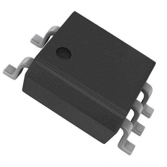
| 描述 | ISOLATOR 3.75KVRMS 1CH 5MFP高速光耦合器 High Noise Immunity 3.3/5V Logic Gat Out |
| 产品分类 | |
| 品牌 | Fairchild Semiconductor |
| 产品手册 | |
| 产品图片 |
|
| rohs | 符合RoHS无铅 / 符合限制有害物质指令(RoHS)规范要求 |
| 产品系列 | 光耦合器/光电耦合器,高速光耦合器,Fairchild Semiconductor FODM8071OPTOPLANAR® |
| 数据手册 | |
| 产品型号 | FODM8071 |
| 上升/下降时间(典型值) | 5.8ns, 5.3ns |
| 上升时间 | 5.8 ns |
| 产品目录页面 | |
| 产品种类 | 高速光耦合器 |
| 传播延迟tpLH/tpHL(最大值) | 55ns, 55ns |
| 供应商器件封装 | 5-MFP |
| 共模瞬态抗扰度(最小值) | 20kV/µs |
| 其它名称 | FODM8071CT |
| 包装 | 散装 |
| 单位重量 | 120 mg |
| 商标 | Fairchild Semiconductor |
| 安装类型 | 表面贴装 |
| 封装 | Bulk |
| 封装/外壳 | 5-MFP |
| 封装/箱体 | SO-5 |
| 工作温度 | -40°C ~ 110°C |
| 工厂包装数量 | 3000 |
| 数据速率 | 20 MBd |
| 最大功率耗散 | 40 mW |
| 最大反向二极管电压 | 5 V |
| 最大工作温度 | + 110 C |
| 最小工作温度 | - 40 C |
| 标准包装 | 3,000 |
| 电压-正向(Vf)(典型值) | 1.35V |
| 电压-电源 | 3 V ~ 5.5 V |
| 电压-隔离 | 3750Vrms |
| 电流-DC正向(If) | 20mA |
| 电流-输出/通道 | 10mA |
| 系列 | FODM8071 |
| 绝缘电压 | 3750 Vrms |
| 输入-输入侧1/输入侧2 | 1/0 |
| 输入类型 | DC |
| 输出类型 | 推挽式/图腾柱 |
| 输出设备 | Photo IC |
| 通道数 | 1 |


- 商务部:美国ITC正式对集成电路等产品启动337调查
- 曝三星4nm工艺存在良率问题 高通将骁龙8 Gen1或转产台积电
- 太阳诱电将投资9.5亿元在常州建新厂生产MLCC 预计2023年完工
- 英特尔发布欧洲新工厂建设计划 深化IDM 2.0 战略
- 台积电先进制程称霸业界 有大客户加持明年业绩稳了
- 达到5530亿美元!SIA预计今年全球半导体销售额将创下新高
- 英特尔拟将自动驾驶子公司Mobileye上市 估值或超500亿美元
- 三星加码芯片和SET,合并消费电子和移动部门,撤换高东真等 CEO
- 三星电子宣布重大人事变动 还合并消费电子和移动部门
- 海关总署:前11个月进口集成电路产品价值2.52万亿元 增长14.8%
PDF Datasheet 数据手册内容提取
Is Now Part of To learn more about ON Semiconductor, please visit our website at www.onsemi.com Please note: As part of the Fairchild Semiconductor integration, some of the Fairchild orderable part numbers will need to change in order to meet ON Semiconductor’s system requirements. Since the ON Semiconductor product management systems do not have the ability to manage part nomenclature that utilizes an underscore (_), the underscore (_) in the Fairchild part numbers will be changed to a dash (-). This document may contain device numbers with an underscore (_). Please check the ON Semiconductor website to verify the updated device numbers. The most current and up-to-date ordering information can be found at www.onsemi.com. Please email any questions regarding the system integration to Fairchild_questions@onsemi.com. ON Semiconductor and the ON Semiconductor logo are trademarks of Semiconductor Components Industries, LLC dba ON Semiconductor or its subsidiaries in the United States and/or other countries. ON Semiconductor owns the rights to a number of patents, trademarks, copyrights, trade secrets, and other intellectual property. A listing of ON Semiconductor’s product/patent coverage may be accessed at www.onsemi.com/site/pdf/Patent-Marking.pdf. ON Semiconductor reserves the right to make changes without further notice to any products herein. ON Semiconductor makes no warranty, representation or guarantee regarding the suitability of its products for any particular purpose, nor does ON Semiconductor assume any liability arising out of the application or use of any product or circuit, and specifically disclaims any and all liability, including without limitation special, consequential or incidental damages. Buyer is responsible for its products and applications using ON Semiconductor products, including compliance with all laws, regulations and safety requirements or standards, regardless of any support or applications information provided by ON Semiconductor. “Typical” parameters which may be provided in ON Semiconductor data sheets and/or specifications can and do vary in different applications and actual performance may vary over time. All operating parameters, including “Typicals” must be validated for each customer application by customer’s technical experts. ON Semiconductor does not convey any license under its patent rights nor the rights of others. ON Semiconductor products are not designed, intended, or authorized for use as a critical component in life support systems or any FDA Class 3 medical devices or medical devices with a same or similar classification in a foreign jurisdiction or any devices intended for implantation in the human body. Should Buyer purchase or use ON Semiconductor products for any such unintended or unauthorized application, Buyer shall indemnify and hold ON Semiconductor and its officers, employees, subsidiaries, affiliates, and distributors harmless against all claims, costs, damages, and expenses, and reasonable attorney fees arising out of, directly or indirectly, any claim of personal injury or death associated with such unintended or unauthorized use, even if such claim alleges that ON Semiconductor was negligent regarding the design or manufacture of the part. ON Semiconductor is an Equal Opportunity/Affirmative Action Employer. This literature is subject to all applicable copyright laws and is not for resale in any manner.
F O D M December 2014 8 0 7 1 — 3 FODM8071 . 3 V 3.3V/5V Logic Gate Output Optocoupler with / 5 V High Noise Immunity L o g i c Features Description G a ■ High-noise Immunity Characterized by Common The FODM8071 is a 3.3V/5V high-speed logic gate t e Mode Rejection output optocoupler, which supports isolated communica- O – 20 kV/µs Minimum Common Mode Rejection tions allowing digital signals to communicate between u systems without conducting ground loops or hazardous t ■ High Speed p voltages. It utilizes Fairchild’s patented coplanar packag- u – 20 Mbit/s Date Rate (NRZ) ing technology, Optoplanar®, and optimized IC design to t O – 55 ns Maximum Propagation Delay achieve high-immunity, characterized by high common p – 20 ns Maximum Pulse Width Distortion mode rejection specifications. to – 30 ns Maximum Propagation Delay Skew c This high-speed logic gate output optocoupler, housed in o ■ 3.3 V and 5 V CMOS Compatibility a compact 5-pin Mini-Flat package, consists of a high- u p ■ Specifications Guaranteed Over 3 V to 5.5 V Supply speed AlGaAs LED at the input coupled to a CMOS l e Voltage and -40°C to +110°C Temperature Range detector IC at the output. The detector IC comprises an r w ■ Safety and Regulatory Approvals: integrated photodiode, a high-speed transimpedance i – UL1577, 3750 VAC for 1 Minute amplifier and a voltage comparator with an output driver. th RMS The CMOS technology coupled with a high-efficiency H – DIN EN/IEC60747-5-5 LED achieves low power consumption as well as very ig high speed (55 ns propagation delay, 20 ns pulse width h Applications distortion). N o ■ Microprocessor System Interface: i Related Resources s – SPI, I2C e ■ Industrial Fieldbus Communications: ■ FOD8001 Product Folder Im – DeviceNet, CAN, RS485 ■ FOD0721 Product Folder m u ■ Programmable Logic Control n ■ Isolated Data Acquisition System it y ■ Voltage Level Translator Schematic and Package Outline Truth Table ANODE 1 6 VDD LED Output Off High 5 VO On Low CATHODE 3 4 GND Figure 1. Schematic and Package Outline ©2008 Fairchild Semiconductor Corporation www.fairchildsemi.com FODM8071 Rev. 1.5
F O Safety and Insulation Ratings D M As per DIN EN/IEC 60747-5-5, this optocoupler is suitable for “safe electrical insulation” only within the safety limit 8 data. Compliance with the safety ratings shall be ensured by means of protective circuits. 0 7 1 Parameter Characteristics — Installation Classifications per DIN VDE < 150 VRMS I–IV 3 . 0110/1.89 Table 1, For Rated Mains Voltage < 300 V I–III 3 RMS V / Climatic Classification 40/110/21 5 V Pollution Degree (DIN VDE 0110/1.89) 2 L o Comparative Tracking Index 175 g i c G a Symbol Parameter Value Unit t e Input-to-Output Test Voltage, Method A, VIORM x 1.6 = VPR, 904 V O Type and Sample Test with t = 10 s, Partial Discharge < 5 pC peak u m V t PR p Input-to-Output Test Voltage, Method B, V x 1.875 = V , IORM PR 1060 V u 100% Production Test with t = 1 s, Partial Discharge < 5 pC peak t m O VIORM Maximum Working Insulation Voltage 565 Vpeak p t V Highest Allowable Over-Voltage 4000 V o IOTM peak c External Creepage ≥ 5 mm o u External Clearance ≥ 5 mm p l e DTI Distance Through Insulation (Insulation Thickness) ≥ 0.4 mm r w TS Case Temperature(1) 150 °C it h I Input Current(1) 200 mA S,INPUT H PS,OUTPUT Output Power(1) 300 mW ig h R Insulation Resistance at T , V = 500 V(1) > 109 Ω IO S IO N o Note: i s 1. Safety limit values – maximum values allowed in the event of a failure. e I m m u n i t y ©2008 Fairchild Semiconductor Corporation www.fairchildsemi.com FODM8071 Rev. 1.5 2
F O Pin Definitions D M Number Name Function Description 8 0 1 ANODE Anode 7 1 3 CATHODE Cathode — 4 GND Output Ground 3 . 3 5 V Output Voltage O V / 6 V Output Supply Voltage 5 DD V L Absolute Maximum Ratings o g i c Stresses exceeding the absolute maximum ratings may damage the device. The device may not function or be G operable above the recommended operating conditions and stressing the parts to these levels is not recommended. a In addition, extended exposure to stresses above the recommended operating conditions may affect device reliability. t e The absolute maximum ratings are stress ratings only. T = 25ºC unless otherwise specified. A O u Symbol Parameter Value Unit t p T Storage Temperature -40 to +125 ºC u STG t T Operating Temperature -40 to +110 ºC O OPR p T Junction Temperature -40 to +125 ºC t J o c TSOL Lead Solder Temperature (Refer to Reflow Temperature Profile) 260 for 10 seconds ºC o u IF Forward Current 20 mA p l V Reverse Voltage 5 V e R r V Supply Voltage 0 to 6.0 V w DD i t V Output Voltage -0.5 to V +0.5 V h O DD H I Average Output Current 10 mA O ig PD Input Power Dissipation(2)(4) 40 mW h I N PD Output Power Dissipation(3)(4) 70 mW O o i s Notes: e 2. Derate linearly from 95˚C at a rate of -1.4 mW/˚C I m 3. Derate linearly from 100˚C at a rate of -3.47 mW/˚C. m u 4. Functional operation under these conditions is not implied. Permanent damage may occur if the device is subjected n to conditions outside these ratings. i t y Recommended Operating Conditions The Recommended Operating Conditions table defines the conditions for actual device operation. Recommended operating conditions are specified to ensure optimal performance to the datasheet specifications. Fairchild does not recommend exceeding them or designing to Absolute Maximum Ratings. Symbol Parameter Min. Max. Unit T Ambient Operating Temperature -40 +110 ºC A V Supply Voltages(5) 3.0 5.5 V DD V Logic Low Input Voltage 0 0.8 V FL I Logic High Input Current 5 16 mA FH I Logic Low Output Current 0 7 mA OL Note: 5. 0.1µF bypass capacitor must be connected between 4 and 6. ©2008 Fairchild Semiconductor Corporation www.fairchildsemi.com FODM8071 Rev. 1.5 3
F O Electrical Characteristics D M Apply over all recommended conditions.TA = -40ºC to +110ºC, 3.0 V ≤ VDD ≤ 5.5 V, unless otherwise specified. 8 Typical value is measured at T = 25ºC and V = 3.3 V. 0 A DD 7 1 Symbol Parameter Test Conditions Min. Typ. Max. Unit — INPUT CHARACTERISTICS 3 . 3 V Forward Voltage I = 10 mA (Figure 2) 1.05 1.35 1.8 V F F V / Input Reverse 5 BVR Breakdown Voltage IR = 10 µA 5 15 V V L Threshold Input o IFHL Current (Figure 3) 2.8 5.0 mA gi c OUTPUT CHARACTERISTICS G a VDD = 3.3 V, IF = 10 mA 3.3 4.8 mA te Logic Low Output (Figures 4 and 6) I O DDL Supply Current V = 5.0 V, I = 10 mA u DD F 4.0 5.0 mA t (Figures 4 and 7) p u Logic High Output VDD = 3.3 V, IF = 0 mA (Figure 5) 3.3 4.8 mA t I O DDH Supply Current VDD = 5.0 V, IF = 0 mA (Figure 5) 4.0 5.0 mA p t V = 3.3 V, I = -20 µA, I = 0 mA V – 0.1 V 3.3 V o DD O F DD c o Logic High Output VDD = 3.3 V, IO = -4 mA, IF = 0 mA VDD – 0.5 V 3.1 V u V OH Voltage V = 5.0 V, I = -20 µA, I = 0 mA V – 0.1 V 5.0 V p DD O F DD l e V = 5.0 V, I = -4 mA, I = 0 mA V – 0.5 V 4.9 V r DD O F DD w Logic Low Output IO = 20 µA, IF = 10 mA 0.0027 0.01 V it VOL Voltage I = 4 mA, I = 10 mA 0.27 0.80 V h O F H i g h N o i s e I m m u n i t y ©2008 Fairchild Semiconductor Corporation www.fairchildsemi.com FODM8071 Rev. 1.5 4
F O Electrical Characteristics (Continued) D M Apply over all recommended conditions.TA = -40ºC to +110ºC, 3.0 V ≤ VDD ≤ 5.5 V, unless otherwise specified. 8 Typical value is measured at T = 25ºC and V = 3.3 V. 0 A DD 7 1 Switching Characteristics — Symbol Parameter Test Conditions Min. Typ. Max. Unit 3 . Date Rate(6) 20 Mbps 3 V / t Pulse Width 50 ns 5 PW V t Propagation Delay Time CL = 15 pF 31 55 ns L PHL to Logic Low Output (Figures 8, 9, and 13) o g t Propagation Delay Time CL = 15 pF 25 55 ns ic PLH to Logic High Output (Figures 8, 9, and 13) G a PWD Pulse Width Distortion, CL = 15 pF 5.5 20 ns te | tPHL - tPLH| (Figures 10 and 11) O t Propagation Delay Skew C = 15 pF(7) 30 ns u PSK L t p Output Rise Time t (Figure 12 and 13) 5.8 ns u R (10% to 90%) t O Output Fall Time p t (Figure 12 and 13) 5.3 ns F (90% to 10%) to c I = 0 mA, V > 0.8 V , o Common Mode Transient F O DD u |CM | V = 1000 V, T = 25ºC, 20 40 kV/µs H Immunity at Output High CM A p (Figure14)(8) l e r I = 5 mA, V < 0.8 V, Common Mode Transient F O w | CML | Immunity at Output Low VCM = 1000 V, TA = 25ºC, 20 40 kV/µs it (Figure14)(8) h H Output Dynamic Power i g CPDO Dissipation 4 pF h Capacitance(9) N o Notes: i s 6. Data rate is based on 10 MHz, 50% NRZ pattern with a 50 nsec minimum bit time. e I 7. t is equal to the magnitude of the worst case difference in t and/or t that will be seen between any two units m PSK PHL PLH from the same manufacturing date code that are operated at same case temperature (±5°C), at the same operating m conditions, with equal loads (R = 350 Ω and C = 15 pF), and with an input rise time less than 5 ns. u L L n 8. Common mode transient immunity at output high is the maximum tolerable positive dVcm/dt on the leading edge of it y the common mode impulse signal, Vcm, to assure that the output will remain high. Common mode transient immunity at output low is the maximum tolerable negative dVcm/dt on the trailing edge of the common pulse signal, Vcm, to assure that the output will remain low. 9. Unloaded dynamic power dissipation is calculated as follows: C x V x f + I + V where f is switched PD DD DD PD time in MHz. Isolation Characteristics Symbol Parameter Conditions Min. Typ. Max. Unit V Input-Output Isolation f = 60 Hz, t = 1.0 minute, 3750 Vac ISO RMS Voltage I ≤ 10 µA(10)(11) I-O R Isolation Resistance V = 500 V(10) 1011 Ω ISO I-O C Isolation Capacitance V = 0 V, f = 1.0 MHz(10) 0.2 pF ISO I-O Notes: 10.Device is considered a two terminal device: pins 1, and 3 are shorted together and pins 4, 5, and 6 are shorted together. 11.3,750 VAC for 1 minute duration is equivalent to 4,500 VAC for 1 second duration. RMS RMS ©2008 Fairchild Semiconductor Corporation www.fairchildsemi.com FODM8071 Rev. 1.5 5
F O Typical Performance Curves D M 100 4.0 8 0 A) mA) 71 T (m NT ( — RREN 10 URRE 3.5 3 CU D C .3 WARD 1 SHOL 3.0 VDD = 5.0 V V/5 UT FOR UT THRE VDD = 3.3 V V Lo I – INPF 0.1 TA = 110°C TA = 25°C TA = -40°C I – INPFHL 2.5 gic G a 0.010.8 0.9 1.0 1.1 1.2 1.3 1.4 1.5 1.6 2.0-40 -20 0 20 40 60 80 100 te VF – FORWARD VOLTAGE (V) TA – AMBIENT TEMPERATURE (°C) O u Figure 2. Input Forward Current Figure 3. Input Threshold Current t p vs. Forward Voltage vs. Ambient Temperature u t O p W OUTPUT SUPPLY CURRENT (mA) 33445....0505.0 IF = 10 mA VVDDDD == 35..30 VV GH OUTPUT SUPPLY CURRENT (mA) 33445.....05050 IF = 0mA VVDDDD == 53..03 VV tocoupler with Hig GIC LO 2.5 GIC HI 2.5 h N – LODDL 2.0 – LODDH 2.0 oise I -40 -20 0 20 40 60 80 100 I -40 -20 0 20 40 60 80 100 I TA – AMBIENT TEMPERATURE (°C) TA – AMBIENT TEMPERATURE (°C) m m Figure 4. Logic Low Output Supply Current Figure 5. Logic High Output Supply Current u vs. Ambient Temperature vs. Ambient Temperature n i t y 5.0 5.5 Frequency = 10M Hz Frequency = 10 MHz Duty Cycle = 50% Duty Cycle = 50% I – DYNAMIC LOGIC LOW OUTPUT DDLSUPPLY CURRENT (mA) 4433....5050 IVFD =D 1 0= m3.A3 VTA =T 2A5 =° C110°C TA = -40°C I – DYNAMIC LOGIC LOW OUTPUT DDLSUPPLY CURRENT (mA) 5443....0505 IVFD =D 1 0= m5.A0 V TTAA == 2151°0C°C TA = -40°C 2.5 3.0 0 2000 4000 6000 8000 10000 0 2000 4000 6000 8000 10000 f – INPUT FREQUENCY (kHz) f – INPUT FREQUENCY (kHz) Figure 6. Dynamic Logic Low Output Supply Current Figure 7. Dynamic Logic Low Output Supply Current vs. Input Frequency (VDD = 3.3V) vs. Input Frequency (VDD = 5.0V) ©2008 Fairchild Semiconductor Corporation www.fairchildsemi.com FODM8071 Rev. 1.5 6
F O Typical Performance Curves (Continued) D M 50 40 8 Frequency = 10 MHz Frequency = 10 MHz 0 Duty Cycle = 50% Duty Cycle = 50% 7 45 IF = 5 mA TA = 25°C 1 DELAY (ns) 3450 tPHL N DELAY (ns) 3305 tPLH — 3.3 OPAGATION 2350 ttPPLHHL ROPAGATIO 25 ttPPLHH L V/5V L t – PRP 20 tPLH t – PP 1250 tPHL ogic 15 VDD = 3.3 V VDD = 3.3 V G VDD = 5.0 V VDD = 5.0 V a 10-40 -20 TA – 0AMBIEN2T0 TEMP4E0RATUR6E0 (°C) 80 100 104 6 IF – PUL8SE INPUT1 0CURREN1T2 (mA) 14 16 te O u Figure 8. Propagation Delay Figure 9. Propagation Delay t p vs. Ambient Temperature vs. Pulse Input Current u t O p ns) 20 Frequency = 10MHz ns) 15 Frequency = 10MHz to N ( Duty Cycle = 50% N ( Duty Cycle = 50% c TORTIO 15 IF = 5mA TORTIO 12 TA = 25°C oup DIS DIS le H H r WIDT 10 VDD = 3.3V WIDT 9 w LSE LSE VDD = 3.3 V ith PU 5 PU 6 H – t|) – PLH 0 VDD = 5.0V – t|) – PLH 3 VDD = 5.0 V igh N PHL PHL o (| t (| t is -5 0 e -40 -20 0 20 40 60 80 100 4 6 8 10 12 14 16 I TA – AMBIENT TEMPERATURE (°C) IF – PULSE INPUT CURRENT (mA) m m Figure 10. Pulse Width Distortion Figure 11. Pulse Width Distortion u vs. Ambient Temperature vs Pulse Input Current n i t y 10 Frequency = 10 MHz Duty Cycle = 50% 9 IF = 5 mA ns) E ( 8 M TI ALL 7 tR F E, RIS 6 – F tF tR , tR 5 t tF 4 VDD = 3.3 V VDD = 5.0 V 3 -40 -20 0 20 40 60 80 100 TA – AMBIENT TEMPERATURE (°C) Figure 12. Rise and Fall Time vs. Ambient Temperature ©2008 Fairchild Semiconductor Corporation www.fairchildsemi.com FODM8071 Rev. 1.5 7
F O Schematics D M 8 Pulse Gen. VCC 07 tf = tr = 5 ns 1 ZO = 50 Ω — 0.1 μF VO 3 Monitoring . 3 Node V Input CL = 15 pF /5 Monitoring V Node L RIN o g i c G IF = 5 mA a t 50% e Input O u t p tPHL tPLH u t tf tr O p Output 90% 90% t o 50% c 10% 10% o VOL u p l e Figure 13. Test Circuit for Propagation Delay Time, Rise Time and Fall Time r w i t h H i IF g h VDD N 0.1 μF o Bypass i s A Output e (Vo) B Im VFF m u n i t VCM y Pulse Gen VCM GND VOH CMH Switching Pos. (A), IF = 0 0.8 x VDD 0.8V VOL Switching Pos. (B), IF = 5 mA CML Figure 14. Test Circuit for Instantaneous Common Mode Rejection Voltage ©2008 Fairchild Semiconductor Corporation www.fairchildsemi.com FODM8071 Rev. 1.5 8
F O Reflow Profile D M 8 Max. Ramp-up Rate = 3°C/S 0 TP Max. Ramp-down Rate = 6°C/S 7 260 1 240 tP — 220 TL 3 . 200 Tsmax 3 tL V C) 180 Preheat Area /5 °e ( 160 Tsmin V L ur 140 ts og t 120 a i r c e 100 p G m 80 a t e e T 60 O 40 u t 20 p u 0 t 120 240 360 O p Time 25°C to Peak to c Time (seconds) o u p Figure 15. Reflow Profile l e r Profile Feature Pb-Free Assembly Profile w i Temperature Min. (Tsmin) 150°C th H Temperature Max. (Tsmax) 200°C i g Time (tS) from (Tsmin to Tsmax) 60–120 seconds h N Ramp-up Rate (t to t ) 3°C/second maximum L P o Liquidous Temperature (TL) 217°C is e Time (tL) Maintained Above (TL) 60–150 seconds Im Peak Body Package Temperature 260°C +0°C / –5°C m Time (t ) within 5°C of 260°C 30 seconds u P n i Ramp-down Rate (T to T ) 6°C/second maximum t P L y Time 25°C to Peak Temperature 8 minutes maximum ©2008 Fairchild Semiconductor Corporation www.fairchildsemi.com FODM8071 Rev. 1.5 9
F O Ordering Information D M Part Number Package Packing Method 8 0 7 FODM8071 Mini-Flat 5-Pin Tube (100 Units) 1 FODM8071R2 Mini-Flat 5-Pin Tape and Reel (2500 Units) — FODM8071V Mini-Flat 5-Pin, DIN EN/IEC60747-5-5 Option Tube (100 Units) 3 . 3 FODM8071R2V Mini-Flat 5-Pin, DIN EN/IEC60747-5-5 Option Tape and Reel (2500 Units) V / 5 V All packages are lead free per JEDEC: J-STD-020B standard. L o g Marking Information ic G a t e O u 1 tp u t M8071 2 O p t o VV X YY M 6 c o u p l e r 3 4 5 w i t h Figure 16. Top Mark H i g h Table 1. Top Mark Definitions N o 1 Fairchild Logo i s 2 Device Number e I m 3 DIN EN/IEC60747-5-5 Option (only appears on component ordered with this option) m 4 One-Digit Year Code, e.g., “4” u n 5 Digit Work Week, Ranging from “01” to “53” i t y 6 Assembly Package Code ©2008 Fairchild Semiconductor Corporation www.fairchildsemi.com FODM8071 Rev. 1.5 10
F O Package Dimensions D M 8 0 7 1 — 3 . 3 V / 5 V L o g i c G a t e O u t p u t O p t o c o u p l e r w i t h H i g h N o i s e I m m u n i t y Figure 17. MLP 5L Package ©2008 Fairchild Semiconductor Corporation www.fairchildsemi.com FODM8071 Rev. 1.5 11
TRADEMARKS The following includes registered and unregistered trademarks and service marks, owned by Fairchild Semiconductor and/or its global subsidiaries, and is not intended to be an exhaustive list of all such trademarks. AccuPower F-PFS OPTOPLANAR® AttitudeEngine™ FRFET® ®* Awinda® Global Power ResourceSM ® TinyBoost® AX-CAP®* GreenBridge Power Supply WebDesigner TinyBuck® BitSiC Green FPS PowerTrench® TinyCalc Build it Now Green FPS e-Series PowerXS™ TinyLogic® CorePLUS Gmax Programmable Active Droop TINYOPTO CorePOWER GTO QFET® TinyPower CROSSVOLT IntelliMAX QS TinyPWM CTL ISOPLANAR Quiet Series TinyWire Current Transfer Logic Making Small Speakers Sound Louder RapidConfigure TranSiC DEUXPEED® and Better™ TriFault Detect Dual Cool™ MegaBuck TRUECURRENT®* EcoSPARK® MICROCOUPLER Saving our world, 1mW/W/kW at a time™ μSerDes EfficientMax MicroFET SignalWise ESBC® MMiiccrrooPPaakk2 SSMmAarRtMT aSxTA RT UHC® Fairchi ld® MillerDrive SSoPlMut®io ns for Your Success Ultra FRFET FFAaiCrcTh iQldu Sieet mSiecroiensduc tor® MMoottiioonnGMraidx® SSTupEeArLFTEHT® UVCniXFET FFAasCtvTC® ore MMMTTVixN®®® SSuuppeerrSSOOTT-3-6 VVXioSsl™utaag lMePalxus FFPESTBe nch mWSaver® SSuuppreerMSOOTS® -8 Xsens™ OOPptToOHLiTOG IC® SyncFET 仙童™ Sync-Lock™ * Trademarks of System General Corporation, used under license by Fairchild Semiconductor. DISCLAIMER FAIRCHILD SEMICONDUCTOR RESERVES THE RIGHT TO MAKE CHANGES WITHOUT FURTHER NOTICE TO ANY PRODUCTS HEREIN TO IMPROVE RELIABILITY, FUNCTION, OR DESIGN. TO OBTAIN THE LATEST, MOST UP-TO-DATE DATASHEET AND PRODUCT INFORMATION, VISIT OUR WEBSITE AT HTTP://WWW.FAIRCHILDSEMI.COM. FAIRCHILD DOES NOT ASSUME ANY LIABILITY ARISING OUT OF THE APPLICATION OR USE OF ANY PRODUCT OR CIRCUIT DESCRIBED HEREIN; NEITHER DOES IT CONVEY ANY LICENSE UNDER ITS PATENT RIGHTS, NOR THE RIGHTS OF OTHERS. THESE SPECIFICATIONS DO NOT EXPAND THE TERMS OF FAIRCHILD’S WORLDWIDE TERMS AND CONDITIONS, SPECIFICALLY THE WARRANTY THEREIN, WHICH COVERS THESE PRODUCTS. AUTHORIZED USE Unless otherwise specified in this data sheet, this product is a standard commercial product and is not intended for use in applications that require extraordinary levels of quality and reliability. This product may not be used in the following applications, unless specifically approved in writing by a Fairchild officer: (1) automotive or other transportation, (2) military/aerospace, (3) any safety critical application – including life critical medical equipment – where the failure of the Fairchild product reasonably would be expected to result in personal injury, death or property damage. Customer’s use of this product is subject to agreement of this Authorized Use policy. In the event of an unauthorized use of Fairchild’s product, Fairchild accepts no liability in the event of product failure. In other respects, this product shall be subject to Fairchild’s Worldwide Terms and Conditions of Sale, unless a separate agreement has been signed by both Parties. ANTI-COUNTERFEITING POLICY Fairchild Semiconductor Corporation's Anti-Counterfeiting Policy. Fairchild's Anti-Counterfeiting Policy is also stated on our external website, www.fairchildsemi.com, under Terms of Use Counterfeiting of semiconductor parts is a growing problem in the industry. All manufacturers of semiconductor products are experiencing counterfeiting of their parts. Customers who inadvertently purchase counterfeit parts experience many problems such as loss of brand reputation, substandard performance, failed applications, and increased cost of production and manufacturing delays. Fairchild is taking strong measures to protect ourselves and our customers from the proliferation of counterfeit parts. Fairchild strongly encourages customers to purchase Fairchild parts either directly from Fairchild or from Authorized Fairchild Distributors who are listed by country on our web page cited above. Products customers buy either from Fairchild directly or from Authorized Fairchild Distributors are genuine parts, have full traceability, meet Fairchild's quality standards for handling and storage and provide access to Fairchild's full range of up-to-date technical and product information. Fairchild and our Authorized Distributors will stand behind all warranties and will appropriately address any warranty issues that may arise. Fairchild will not provide any warranty coverage or other assistance for parts bought from Unauthorized Sources. Fairchild is committed to combat this global problem and encourage our customers to do their part in stopping this practice by buying direct or from authorized distributors. PRODUCT STATUS DEFINITIONS Definition of Terms Datasheet Identification Product Status Definition Datasheet contains the design specifications for product development. Specifications may change Advance Information Formative / In Design in any manner without notice. Datasheet contains preliminary data; supplementary data will be published at a later date. Fairchild Preliminary First Production Semiconductor reserves the right to make changes at any time without notice to improve design. Datasheet contains final specifications. Fairchild Semiconductor reserves the right to make No Identification Needed Full Production changes at any time without notice to improve the design. Datasheet contains specifications on a product that is discontinued by Fairchild Semiconductor. Obsolete Not In Production The datasheet is for reference information only. Rev. I76 © Fairchild Semiconductor Corporation www.fairchildsemi.com
ON Semiconductor and are trademarks of Semiconductor Components Industries, LLC dba ON Semiconductor or its subsidiaries in the United States and/or other countries. ON Semiconductor owns the rights to a number of patents, trademarks, copyrights, trade secrets, and other intellectual property. A listing of ON Semiconductor’s product/patent coverage may be accessed at www.onsemi.com/site/pdf/Patent−Marking.pdf. ON Semiconductor reserves the right to make changes without further notice to any products herein. ON Semiconductor makes no warranty, representation or guarantee regarding the suitability of its products for any particular purpose, nor does ON Semiconductor assume any liability arising out of the application or use of any product or circuit, and specifically disclaims any and all liability, including without limitation special, consequential or incidental damages. Buyer is responsible for its products and applications using ON Semiconductor products, including compliance with all laws, regulations and safety requirements or standards, regardless of any support or applications information provided by ON Semiconductor. “Typical” parameters which may be provided in ON Semiconductor data sheets and/or specifications can and do vary in different applications and actual performance may vary over time. All operating parameters, including “Typicals” must be validated for each customer application by customer’s technical experts. ON Semiconductor does not convey any license under its patent rights nor the rights of others. ON Semiconductor products are not designed, intended, or authorized for use as a critical component in life support systems or any FDA Class 3 medical devices or medical devices with a same or similar classification in a foreign jurisdiction or any devices intended for implantation in the human body. Should Buyer purchase or use ON Semiconductor products for any such unintended or unauthorized application, Buyer shall indemnify and hold ON Semiconductor and its officers, employees, subsidiaries, affiliates, and distributors harmless against all claims, costs, damages, and expenses, and reasonable attorney fees arising out of, directly or indirectly, any claim of personal injury or death associated with such unintended or unauthorized use, even if such claim alleges that ON Semiconductor was negligent regarding the design or manufacture of the part. ON Semiconductor is an Equal Opportunity/Affirmative Action Employer. This literature is subject to all applicable copyright laws and is not for resale in any manner. PUBLICATION ORDERING INFORMATION LITERATURE FULFILLMENT: N. American Technical Support: 800−282−9855 Toll Free ON Semiconductor Website: www.onsemi.com Literature Distribution Center for ON Semiconductor USA/Canada 19521 E. 32nd Pkwy, Aurora, Colorado 80011 USA Europe, Middle East and Africa Technical Support: Order Literature: http://www.onsemi.com/orderlit Phone: 303−675−2175 or 800−344−3860 Toll Free USA/Canada Phone: 421 33 790 2910 Fax: 303−675−2176 or 800−344−3867 Toll Free USA/Canada Japan Customer Focus Center For additional information, please contact your local Email: orderlit@onsemi.com Phone: 81−3−5817−1050 Sales Representative © Semiconductor Components Industries, LLC www.onsemi.com www.onsemi.com 1
Mouser Electronics Authorized Distributor Click to View Pricing, Inventory, Delivery & Lifecycle Information: O N Semiconductor: FODM8071 FODM8071R2