ICGOO在线商城 > 分立半导体产品 > 晶体管 - 双极 (BJT) - 单 > PBSS301ND,115
 Datasheet下载
- 型号: PBSS301ND,115
- 制造商: NXP Semiconductors
- 库位|库存: xxxx|xxxx
- 要求:
| 数量阶梯 | 香港交货 | 国内含税 |
| +xxxx | $xxxx | ¥xxxx |
查看当月历史价格
查看今年历史价格
PBSS301ND,115产品简介:
ICGOO电子元器件商城为您提供PBSS301ND,115由NXP Semiconductors设计生产,在icgoo商城现货销售,并且可以通过原厂、代理商等渠道进行代购。 PBSS301ND,115价格参考。NXP SemiconductorsPBSS301ND,115封装/规格:晶体管 - 双极 (BJT) - 单, 双极 (BJT) 晶体管 NPN 20V 4A 100MHz 1.1W 表面贴装 6-TSOP。您可以下载PBSS301ND,115参考资料、Datasheet数据手册功能说明书,资料中有PBSS301ND,115 详细功能的应用电路图电压和使用方法及教程。
PBSS301ND,115 是由 Nexperia USA Inc. 生产的一款双极型晶体管(BJT),属于单晶体管类型。以下是该型号的应用场景分析:

 1. 低功耗设备
   - PBSS301ND,115 具有低功耗特性,适合应用于便携式电子设备,例如无线耳机、智能手环等。其高效能和小尺寸设计使其成为这些设备的理想选择。

 2. 信号放大
   - 作为一款 BJT 晶体管,PBSS301ND,115 可用于音频信号放大器中。它能够将微弱的输入信号放大到足够的强度,适用于音响系统、麦克风前置放大器和其他需要信号放大的场合。

 3. 开关电路
   - 在数字电路中,PBSS301ND,115 可用作开关元件。它能够在饱和区和截止区之间快速切换,适用于 LED 驱动、继电器控制、电机驱动等场景。

 4. 电源管理
   - 该晶体管可用于简单的电源管理电路中,例如电压调节器或电流限制电路。它能够提供稳定的电流输出,确保下游负载的安全运行。

 5. 消费类电子产品
   - PBSS301ND,115 的紧凑封装和高性能使其广泛应用于消费类电子产品,如电视遥控器、玩具、家用电器控制器等。

 6. 工业控制
   - 在工业自动化领域,这款晶体管可用于传感器信号处理、逻辑电平转换以及小型执行器的驱动。

 7. 通信设备
   - 由于其良好的频率响应特性,PBSS301ND,115 可用于通信设备中的信号调制与解调电路,例如对讲机、无线模块等。

 总结
PBSS301ND,115 凭借其出色的性能参数和可靠性,适用于多种应用场景,包括但不限于低功耗设备、信号放大、开关电路、电源管理、消费类电子产品、工业控制和通信设备等领域。具体应用时需根据实际需求选择合适的外围电路设计以充分发挥其性能优势。
| 参数 | 数值 |
| 产品目录 | |
| 描述 | TRANS NPN 20V 4A LOW SAT 6TSOP |
| 产品分类 | 晶体管(BJT) - 单路 |
| 品牌 | NXP Semiconductors |
| 数据手册 | |
| 产品图片 |
|
| 产品型号 | PBSS301ND,115 |
| PCN封装 | |
| rohs | 无铅 / 符合限制有害物质指令(RoHS)规范要求 |
| 产品系列 | - |
| 不同 Ib、Ic时的 Vce饱和值(最大值) | 420mV @ 600mA,6A |
| 不同 Ic、Vce 时的DC电流增益(hFE)(最小值) | 250 @ 2A,2V |
| 产品培训模块 | http://www.digikey.cn/PTM/IndividualPTM.page?site=cn&lang=zhs&ptm=9367 |
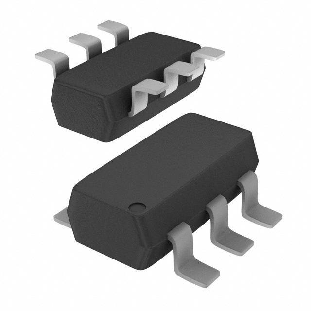
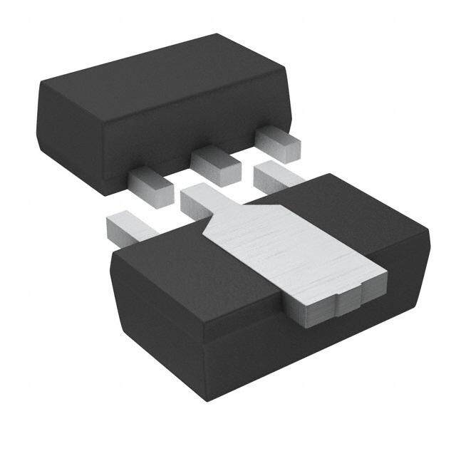
| 供应商器件封装 | 6-TSOP |
| 其它名称 | 568-4149-2 |
| 功率-最大值 | 1.1W |
| 包装 | 带卷 (TR) |
| 安装类型 | 表面贴装 |
| 封装/外壳 | SC-74,SOT-457 |
| 晶体管类型 | NPN |
| 标准包装 | 3,000 |
| 特色产品 | http://www.digikey.com/cn/zh/ph/NXP/I2C.html |
| 电压-集射极击穿(最大值) | 20V |
| 电流-集电极(Ic)(最大值) | 4A |
| 电流-集电极截止(最大值) | 100nA |
| 频率-跃迁 | 100MHz |


PDF Datasheet 数据手册内容提取
Important notice Dear Customer, On 7 February 2017 the former NXP Standard Product business became a new company with the tradename Nexperia. Nexperia is an industry leading supplier of Discrete, Logic and PowerMOS semiconductors with its focus on the automotive, industrial, computing, consumer and wearable application markets In data sheets and application notes which still contain NXP or Philips Semiconductors references, use the references to Nexperia, as shown below. Instead of http://www.nxp.com, http://www.philips.com/ or http://www.semiconductors.philips.com/, use http://www.nexperia.com Instead of sales.addresses@www.nxp.com or sales.addresses@www.semiconductors.philips.com, use salesaddresses@nexperia.com (email) Replace the copyright notice at the bottom of each page or elsewhere in the document, depending on the version, as shown below: - © NXP N.V. (year). All rights reserved or © Koninklijke Philips Electronics N.V. (year). All rights reserved Should be replaced with: - © Nexperia B.V. (year). All rights reserved. If you have any questions related to the data sheet, please contact our nearest sales office via e-mail or telephone (details via salesaddresses@nexperia.com). Thank you for your cooperation and understanding, Kind regards, Team Nexperia
PBSS301ND 20 V, 4 A NPN low V (BISS) transistor CEsat Rev. 03 — 7 September 2007 Product data sheet 1. Product profile 1.1 General description NPN low V Breakthrough in Small Signal (BISS) transistor in a SOT457 (SC-74) CEsat Surface-Mounted Device (SMD) plastic package. PNP complement: PBSS301PD. 1.2 Features n Very low collector-emitter saturation resistance n Ultra low collector-emitter saturation voltage n 4 A continuous collector current n Up to 15 A peak current n High efficiency due to less heat generation 1.3 Applications n Power management functions n Charging circuits n DC-to-DC conversion n MOSFET gate driving n Power switches (e.g. motors, fans) n Thin Film Transistor (TFT) backlight inverter 1.4 Quick reference data Table 1. Quick reference data Symbol Parameter Conditions Min Typ Max Unit V collector-emitter voltage open base - - 20 V CEO I collector current [1] - - 4 A C I peak collector current single pulse; - - 15 A CM t £ 1ms p R collector-emitter saturation I =4A; [2] - 50 70 mW CEsat C resistance I =400mA B [1] Device mounted on a ceramic Printed-Circuit Board (PCB), Al O , standard footprint. 2 3 [2] Pulse test: t £ 300m s;d£ 0.02. p
PBSS301ND NXP Semiconductors 20 V, 4 A NPN low V (BISS) transistor CEsat 2. Pinning information Table 2. Pinning Pin Description Simplified outline Symbol 1 collector 6 5 4 1, 2, 5, 6 2 collector 3 base 3 4 emitter 1 2 3 4 5 collector sym014 6 collector 3. Ordering information Table 3. Ordering information Type number Package Name Description Version PBSS301ND SC-74 plastic surface-mounted package (TSOP6); 6leads SOT457 4. Marking Table 4. Marking codes Type number Marking code PBSS301ND C6 5. Limiting values Table 5. Limiting values In accordance with the Absolute Maximum Rating System (IEC 60134). Symbol Parameter Conditions Min Max Unit V collector-base voltage open emitter - 20 V CBO V collector-emitter voltage open base - 20 V CEO V emitter-base voltage open collector - 5 V EBO I collector current [1] - 4 A C I peak collector current single pulse; - 15 A CM t £ 1ms p I base current - 0.8 A B I peak base current single pulse; - 2 A BM t £ 1ms p P total power dissipation T £ 25(cid:176) C [2] - 360 mW tot amb [3] - 600 mW [4] - 750 mW [1] - 1.1 W [2][5] - 2.5 W PBSS301ND_3 © NXP B.V. 2007. All rights reserved. Product data sheet Rev. 03 — 7 September 2007 2 of 14
PBSS301ND NXP Semiconductors 20 V, 4 A NPN low V (BISS) transistor CEsat Table 5. Limiting values …continued In accordance with the Absolute Maximum Rating System (IEC 60134). Symbol Parameter Conditions Min Max Unit T junction temperature - 150 (cid:176) C j T ambient temperature - 65 +150 (cid:176) C amb T storage temperature - 65 +150 (cid:176) C stg [1] Device mounted on a ceramic PCB, Al O , standard footprint. 2 3 [2] Device mounted on an FR4 PCB, single-sided copper, tin-plated and standard footprint. [3] Device mounted on an FR4 PCB, single-sided copper, tin-plated, mounting pad for collector 1cm2. [4] Device mounted on an FR4 PCB, single-sided copper, tin-plated, mounting pad for collector 6cm2. [5] Operated under pulsed conditions: duty cycled£ 10% and pulse width t £ 10ms. p 006aaa270 1600 Ptot (mW) 1200 (1) 800 (2) (3) 400 (4) 0 - 75 - 25 25 75 125 175 Tamb ((cid:176)C) (1) Ceramic PCB, Al O , standard footprint 2 3 (2) FR4 PCB, mounting pad for collector 6cm2 (3) FR4 PCB, mounting pad for collector 1cm2 (4) FR4 PCB, standard footprint Fig 1. Power derating curves PBSS301ND_3 © NXP B.V. 2007. All rights reserved. Product data sheet Rev. 03 — 7 September 2007 3 of 14
PBSS301ND NXP Semiconductors 20 V, 4 A NPN low V (BISS) transistor CEsat 6. Thermal characteristics Table 6. Thermal characteristics Symbol Parameter Conditions Min Typ Max Unit R thermal resistance from in free air [2] - - 350 K/W th(j-a) junction to ambient [3] - - 208 K/W [4] - - 167 K/W [1] - - 113 K/W [2][5] - - 50 K/W R thermal resistance from - - 45 K/W th(j-sp) junction to solder point [1] Device mounted on a ceramic PCB, Al O , standard footprint. 2 3 [2] Device mounted on an FR4 PCB, single-sided copper, tin-plated and standard footprint. [3] Device mounted on an FR4 PCB, single-sided copper, tin-plated, mounting pad for collector 1cm2. [4] Device mounted on an FR4 PCB, single-sided copper, tin-plated, mounting pad for collector 6cm2. [5] Operated under pulsed conditions: duty cycled£ 10% and pulse width t £ 10ms. p 103 006aaa271 Zth(j-a) duty cycle = 1 (K/W) 0.75 0.5 102 0.33 0.2 0.1 0.05 10 0.02 0.01 1 0 10- 1 10- 5 10- 4 10- 3 10- 2 10- 1 1 10 102 103 tp (s) FR4 PCB, standard footprint Fig 2. Transient thermal impedance from junction to ambient as a function of pulse duration; typical values PBSS301ND_3 © NXP B.V. 2007. All rights reserved. Product data sheet Rev. 03 — 7 September 2007 4 of 14
PBSS301ND NXP Semiconductors 20 V, 4 A NPN low V (BISS) transistor CEsat 103 006aaa272 Zth(j-a) duty cycle = (K/W) 1 0.75 102 0.5 0.33 0.2 0.1 10 0.05 0.02 0.01 1 0 10- 1 10- 5 10- 4 10- 3 10- 2 10- 1 1 10 102 103 tp (s) FR4 PCB, mounting pad for collector 1cm2 Fig 3. Transient thermal impedance from junction to ambient as a function of pulse duration; typical values 103 006aaa273 Zth(j-a) (K/W) duty cycle = 1 102 0.75 0.5 0.33 0.2 0.1 10 0.05 0.02 0.01 1 0 10- 1 10- 5 10- 4 10- 3 10- 2 10- 1 1 10 102 103 tp (s) FR4 PCB, mounting pad for collector 6cm2 Fig 4. Transient thermal impedance from junction to ambient as a function of pulse duration; typical values PBSS301ND_3 © NXP B.V. 2007. All rights reserved. Product data sheet Rev. 03 — 7 September 2007 5 of 14
PBSS301ND NXP Semiconductors 20 V, 4 A NPN low V (BISS) transistor CEsat 7. Characteristics Table 7. Characteristics T =25(cid:176) C unless otherwise specified. amb Symbol Parameter Conditions Min Typ Max Unit I collector-base cut-off V =20V; I =0A - - 0.1 m A CBO CB E current V =20V; I =0A; - - 50 m A CB E T =150(cid:176) C j I collector-emittercut-off V =20V; V =0V - - 0.1 m A CES CE BE current I emitter-base cut-off V =5V; I =0A - - 0.1 m A EBO EB C current h DC current gain V =2V; I =0.5A 300 450 - FE CE C V =2V; I =1A [1] 300 430 - CE C V =2V; I =2A [1] 250 400 - CE C V =2V; I =4A [1] 200 310 - CE C V =2V; I =6A [1] 100 230 - CE C V collector-emitter I =0.5A; I =50mA - 30 50 mV CEsat C B saturation voltage I =1A; I =50mA - 60 90 mV C B I =2A; I =200mA - 110 150 mV C B I =4A; I =400mA [1] - 200 280 mV C B I =6A; I =600mA [1] - 300 420 mV C B R collector-emitter I =4A; I =400mA [1] - 50 70 mW CEsat C B saturation resistance V base-emittersaturation I =0.5A; I =50mA - 0.79 0.85 V BEsat C B voltage I =1A; I =50mA - 0.81 0.9 V C B I =1A; I =100mA [1] - 0.83 1 V C B I =4A; I =400mA [1] - 1.0 1.1 V C B V base-emitter turn-on V =2V; I =2A - 0.79 1 V BEon CE C voltage t delay time V =12.5V; I =3A; - 12 - ns d CC C I =0.15A; t rise time Bon - 36 - ns r I =- 0.15A Boff t turn-on time - 48 - ns on t storage time - 230 - ns s t fall time - 50 - ns f t turn-off time - 280 - ns off f transition frequency V =10V; I =0.1A; - 100 - MHz T CE C f=100MHz C collector capacitance V =10V; I =i =0A; - 60 - pF c CB E e f=1MHz [1] Pulse test: t £ 300m s;d£ 0.02. p PBSS301ND_3 © NXP B.V. 2007. All rights reserved. Product data sheet Rev. 03 — 7 September 2007 6 of 14
PBSS301ND NXP Semiconductors 20 V, 4 A NPN low V (BISS) transistor CEsat 006aaa328 006aaa334 1000 10 IB (mA) = 80 hFE IC 72 (A) 64 800 8 56 48 (1) 40 32 600 6 24 (2) 16 400 4 (3) 8 200 2 0 0 10- 1 1 10 102 103 104 105 0 0.4 0.8 1.2 1.6 2.0 IC (mA) VCE (V) V =2V T =25(cid:176) C CE amb (1) T =100(cid:176) C amb (2) T =25(cid:176) C amb (3) T =- 55(cid:176) C amb Fig 5. DC current gain as a function of collector Fig 6. Collector current as a function of current; typical values collector-emitter voltage; typical values 006aaa329 006aaa332 1.4 1.5 VBE VBEsat (V) (V) 1.2 1.3 1.0 1.1 0.8 (1) 0.9 (1) (2) 0.6 0.7 (2) (3) (3) 0.4 0.5 0.2 0.3 0 0.1 10- 1 1 10 102 103 104 105 10- 1 1 10 102 103 104 105 IC (mA) IC (mA) V =2V I /I =20 CE C B (1) T =- 55(cid:176) C (1) T =- 55(cid:176) C amb amb (2) T =25(cid:176) C (2) T =25(cid:176) C amb amb (3) T =100(cid:176) C (3) T =100(cid:176) C amb amb Fig 7. Base-emitter voltage as a function of collector Fig 8. Base-emittersaturationvoltageasafunctionof current; typical values collector current; typical values PBSS301ND_3 © NXP B.V. 2007. All rights reserved. Product data sheet Rev. 03 — 7 September 2007 7 of 14
PBSS301ND NXP Semiconductors 20 V, 4 A NPN low V (BISS) transistor CEsat 006aaa330 006aaa331 10 10 VCEsat VCEsat (V) (V) 1.0 1 (1) 10- 1 (2) 10- 1 (3) (1) 10- 2 10- 2 (2) (3) 10- 3 10- 3 10- 1 1 10 102 103 104 105 10- 1 1 10 102 103 104 105 IC (mA) IC (mA) I /I =20 T =25(cid:176) C C B amb (1) T =100(cid:176) C (1) I /I =100 amb C B (2) T =25(cid:176) C (2) I /I =50 amb C B (3) T =- 55(cid:176) C (3) I /I =10 amb C B Fig 9. Collector-emitter saturation voltage as a Fig 10. Collector-emitter saturation voltage as a function of collector current; typical values function of collector current; typical values 102 006aaa335 103 006aaa333 RC(WE)sat RC(WE)sat 102 10 (1) 10 1 (2) 1 (1) (3) (2) 10- 1 (3) 10- 1 10- 2 10- 2 10- 1 1 10 102 103 104 105 10- 1 1 10 102 103 104 105 IC (mA) IC (mA) I /I =20 T =25(cid:176) C C B amb (1) T =100(cid:176) C (1) I /I =100 amb C B (2) T =25(cid:176) C (2) I /I =50 amb C B (3) T =- 55(cid:176) C (3) I /I =10 amb C B Fig 11. Collector-emitter saturation resistance as a Fig 12. Collector-emitter saturation resistance as a function of collector current; typical values function of collector current; typical values PBSS301ND_3 © NXP B.V. 2007. All rights reserved. Product data sheet Rev. 03 — 7 September 2007 8 of 14
PBSS301ND NXP Semiconductors 20 V, 4 A NPN low V (BISS) transistor CEsat 8. Test information IB 90 % input pulse (idealized waveform) IBon (100 %) 10 % IBoff output pulse IC (idealized waveform) 90 % IC (100 %) 10 % t td tr ts tf ton toff 006aaa003 Fig 13. BISS transistor switching time definition VBB VCC RB RC (probe) Vo (probe) oscilloscope oscilloscope 450 W 450 W R2 VI DUT R1 mlb826 V =12.5V; I =3A; I =0.15A; I =- 0.15A CC C Bon Boff Fig 14. Test circuit for switching times PBSS301ND_3 © NXP B.V. 2007. All rights reserved. Product data sheet Rev. 03 — 7 September 2007 9 of 14
PBSS301ND NXP Semiconductors 20 V, 4 A NPN low V (BISS) transistor CEsat 9. Package outline 3.1 1.1 2.7 0.9 6 5 4 0.6 0.2 3.0 1.7 2.5 1.3 pin 1 index 1 2 3 0.40 0.26 0.95 0.25 0.10 1.9 Dimensions in mm 04-11-08 Fig 15. Package outline SOT457 (SC-74) 10. Packing information Table 8. Packing methods The indicated -xxx are the last three digits of the 12NC ordering code.[1] Type number Package Description Packing quantity 3000 10000 PBSS301ND SOT457 4mm pitch, 8mm tape and reel; T1 [2] -115 -135 4mm pitch, 8mm tape and reel; T2 [3] -125 -165 [1] For further information and the availability of packing methods, seeSection14. [2] T1: normal taping [3] T2: reverse taping PBSS301ND_3 © NXP B.V. 2007. All rights reserved. Product data sheet Rev. 03 — 7 September 2007 10 of 14
PBSS301ND NXP Semiconductors 20 V, 4 A NPN low V (BISS) transistor CEsat 11. Soldering 3.45 1.95 solder lands 0.95 solder resist 3.30 2.825 0.45 0.55 occupied area solder paste 1.60 1.70 3.10 3.20 msc422 Dimensions in mm Fig 16. Reflow soldering footprint SOT457 (SC-74) 5.30 solder lands 5.05 0.45 1.45 4.45 solder resist occupied area 1.40 msc423 4.30 Dimensions in mm Fig 17. Wave soldering footprint SOT457 (SC-74) PBSS301ND_3 © NXP B.V. 2007. All rights reserved. Product data sheet Rev. 03 — 7 September 2007 11 of 14
PBSS301ND NXP Semiconductors 20 V, 4 A NPN low V (BISS) transistor CEsat 12. Revision history Table 9. Revision history Document ID Release date Data sheet status Change notice Supersedes PBSS301ND_3 20070907 Product data sheet - PBSS301ND_2 Modifications: • The format of this data sheet has been redesigned to comply with the new identity guidelines of NXP Semiconductors. • Legal texts have been adapted to the new company name where appropriate. • Section 1.1 “General description”: amended • Table6: typing error for maximum value on 6cm2 footprint amended • Figure2,3,4,6 and7: amended • Figure15: superseded by minimized package outline drawing • Section 11 “Soldering”: added • Section 13 “Legal information”: updated PBSS301ND_2 20050425 Product data sheet - PBSS301ND_1 PBSS301ND_1 20050405 Product data sheet - - PBSS301ND_3 © NXP B.V. 2007. All rights reserved. Product data sheet Rev. 03 — 7 September 2007 12 of 14
PBSS301ND NXP Semiconductors 20 V, 4 A NPN low V (BISS) transistor CEsat 13. Legal information 13.1 Data sheet status Document status[1][2] Product status[3] Definition Objective [short] data sheet Development This document contains data from the objective specification for product development. Preliminary [short] data sheet Qualification This document contains data from the preliminary specification. Product [short] data sheet Production This document contains the product specification. [1] Please consult the most recently issued document before initiating or completing a design. [2] The term ‘short data sheet’ is explained in section “Definitions”. [3] Theproductstatusofdevice(s)describedinthisdocumentmayhavechangedsincethisdocumentwaspublishedandmaydifferincaseofmultipledevices.Thelatestproductstatus information is available on the Internet at URLhttp://www.nxp.com. 13.2 Definitions malfunctionofaNXPSemiconductorsproductcanreasonablybeexpectedto result in personal injury, death or severe property or environmental damage. NXP Semiconductors accepts no liability for inclusion and/or use of NXP Draft —The document is a draft version only. The content is still under Semiconductors products in such equipment or applications and therefore internal review and subject to formal approval, which may result in such inclusion and/or use is at the customer’s own risk. modifications or additions. NXP Semiconductors does not give any representations or warranties as to the accuracy or completeness of Applications —Applications that are described herein for any of these informationincludedhereinandshallhavenoliabilityfortheconsequencesof products are for illustrative purposes only. NXP Semiconductors makes no use of such information. representation or warranty that such applications will be suitable for the specified use without further testing or modification. Short data sheet —A short data sheet is an extract from a full data sheet withthesameproducttypenumber(s)andtitle.Ashortdatasheetisintended Limiting values —Stress above one or more limiting values (as defined in forquickreferenceonlyandshouldnotbereliedupontocontaindetailedand theAbsoluteMaximumRatingsSystemofIEC60134)maycausepermanent full information. For detailed and full information see the relevant full data damagetothedevice.Limitingvaluesarestressratingsonlyandoperationof sheet, which is available on request via the local NXP Semiconductors sales the device at these or any other conditions above those given in the office. In case of any inconsistency or conflict with the short data sheet, the Characteristics sections of this document is not implied. Exposure to limiting full data sheet shall prevail. values for extended periods may affect device reliability. Terms and conditions of sale —NXP Semiconductors products are sold 13.3 Disclaimers subjecttothegeneraltermsandconditionsofcommercialsale,aspublished athttp://www.nxp.com/profile/terms, including those pertaining to warranty, intellectual property rights infringement and limitation of liability, unless General —Information in this document is believed to be accurate and explicitly otherwise agreed to in writing by NXP Semiconductors. In case of reliable.However,NXPSemiconductorsdoesnotgiveanyrepresentationsor any inconsistency or conflict between information in this document and such warranties,expressedorimplied,astotheaccuracyorcompletenessofsuch terms and conditions, the latter will prevail. information and shall have no liability for the consequences of use of such No offer to sell or license —Nothing in this document may be interpreted information. or construed as an offer to sell products that is open for acceptance or the Right to make changes —NXPSemiconductorsreservestherighttomake grant,conveyanceorimplicationofanylicenseunderanycopyrights,patents changes to information published in this document, including without or other industrial or intellectual property rights. limitation specifications and product descriptions, at any time and without notice.Thisdocumentsupersedesandreplacesallinformationsuppliedprior to the publication hereof. 13.4 Trademarks Suitability for use —NXP Semiconductors products are not designed, Notice:Allreferencedbrands,productnames,servicenamesandtrademarks authorized or warranted to be suitable for use in medical, military, aircraft, are the property of their respective owners. space or life support equipment, nor in applications where failure or 14. Contact information For additional information, please visit:http://www.nxp.com For sales office addresses, send an email to:salesaddresses@nxp.com PBSS301ND_3 © NXP B.V. 2007. All rights reserved. Product data sheet Rev. 03 — 7 September 2007 13 of 14
PBSS301ND NXP Semiconductors 20 V, 4 A NPN low V (BISS) transistor CEsat 15. Contents 1 Product profile. . . . . . . . . . . . . . . . . . . . . . . . . . 1 1.1 General description. . . . . . . . . . . . . . . . . . . . . . 1 1.2 Features . . . . . . . . . . . . . . . . . . . . . . . . . . . . . . 1 1.3 Applications . . . . . . . . . . . . . . . . . . . . . . . . . . . 1 1.4 Quick reference data. . . . . . . . . . . . . . . . . . . . . 1 2 Pinning information. . . . . . . . . . . . . . . . . . . . . . 2 3 Ordering information. . . . . . . . . . . . . . . . . . . . . 2 4 Marking. . . . . . . . . . . . . . . . . . . . . . . . . . . . . . . . 2 5 Limiting values. . . . . . . . . . . . . . . . . . . . . . . . . . 2 6 Thermal characteristics. . . . . . . . . . . . . . . . . . . 4 7 Characteristics. . . . . . . . . . . . . . . . . . . . . . . . . . 6 8 Test information. . . . . . . . . . . . . . . . . . . . . . . . . 9 9 Package outline . . . . . . . . . . . . . . . . . . . . . . . . 10 10 Packing information. . . . . . . . . . . . . . . . . . . . . 10 11 Soldering . . . . . . . . . . . . . . . . . . . . . . . . . . . . . 11 12 Revision history. . . . . . . . . . . . . . . . . . . . . . . . 12 13 Legal information. . . . . . . . . . . . . . . . . . . . . . . 13 13.1 Data sheet status . . . . . . . . . . . . . . . . . . . . . . 13 13.2 Definitions. . . . . . . . . . . . . . . . . . . . . . . . . . . . 13 13.3 Disclaimers. . . . . . . . . . . . . . . . . . . . . . . . . . . 13 13.4 Trademarks. . . . . . . . . . . . . . . . . . . . . . . . . . . 13 14 Contact information. . . . . . . . . . . . . . . . . . . . . 13 15 Contents. . . . . . . . . . . . . . . . . . . . . . . . . . . . . . 14 Pleasebeawarethatimportantnoticesconcerningthisdocumentandtheproduct(s) described herein, have been included in section ‘Legal information’. © NXP B.V. 2007. All rights reserved. For more information, please visit: http://www.nxp.com For sales office addresses, please send an email to: salesaddresses@nxp.com Date of release: 7 September 2007 Document identifier: PBSS301ND_3