ICGOO在线商城 > 集成电路(IC) > 线性 - 放大器 - 仪表,运算放大器,缓冲器放大器 > OPA343UA
 Datasheet下载
- 型号: OPA343UA
- 制造商: Texas Instruments
- 库位|库存: xxxx|xxxx
- 要求:
| 数量阶梯 | 香港交货 | 国内含税 |
| +xxxx | $xxxx | ¥xxxx |
查看当月历史价格
查看今年历史价格
OPA343UA产品简介:
ICGOO电子元器件商城为您提供OPA343UA由Texas Instruments设计生产,在icgoo商城现货销售,并且可以通过原厂、代理商等渠道进行代购。 OPA343UA价格参考。Texas InstrumentsOPA343UA封装/规格:线性 - 放大器 - 仪表,运算放大器,缓冲器放大器, 通用 放大器 1 电路 满摆幅 8-SOIC。您可以下载OPA343UA参考资料、Datasheet数据手册功能说明书,资料中有OPA343UA 详细功能的应用电路图电压和使用方法及教程。
Texas Instruments的OPA343UA是一款超低功耗、零漂移运算放大器,适用于多种精密信号处理应用。其特点包括极低的输入偏置电流、低噪声和高精度,使其在电池供电设备和便携式仪器中表现出色。

 应用场景

1. 医疗设备:
   - 心电图(ECG)监测:OPA343UA的低功耗和高精度特性非常适合用于ECG设备中的前置放大器,确保信号的准确性和稳定性。
   - 血糖仪:在血糖仪中,该放大器可以提供稳定的信号放大,确保测量结果的准确性。

2. 工业自动化:
   - 传感器接口:用于温度、压力、位移等传感器的信号调理电路中,OPA343UA能够提供高精度的信号放大和处理,适应恶劣的工业环境。
   - 数据采集系统:在工业控制系统中,该放大器可用于将微弱的模拟信号放大并转换为适合后续处理的电平。

3. 消费电子:
   - 便携式音频设备:如无线耳机、便携式音箱等,OPA343UA的低功耗特性有助于延长电池寿命,同时保持音质的清晰度。
   - 智能家居传感器:用于环境监测、安防监控等智能家居设备中,提供稳定可靠的信号放大。

4. 汽车电子:
   - 车载传感器:如胎压监测系统(TPMS)、车身稳定控制系统(ESC)等,OPA343UA可以提供精确的信号放大,确保系统的可靠性和安全性。
   - 车载信息娱乐系统:在车载音响和其他娱乐设备中,该放大器能够提供高质量的音频信号处理。

5. 科学仪器:
   - 实验室测试设备:如示波器、频谱分析仪等,OPA343UA可以用于前端信号调理,确保测量结果的准确性和可靠性。
   - 精密测量仪器:在需要高精度测量的应用中,如微小电流或电压的测量,该放大器能够提供出色的性能。

总之,OPA343UA凭借其低功耗、高精度和稳定性,广泛应用于各种对信号处理要求较高的领域,特别是在需要长时间稳定工作且对功耗敏感的场合表现尤为突出。
| 参数 | 数值 |
| -3db带宽 | - |
| 产品目录 | 集成电路 (IC)半导体 |
| 描述 | IC OPAMP GP 5.5MHZ RRO 8SOIC运算放大器 - 运放 Single-Supply Rail-to-Rail |
| 产品分类 | Linear - Amplifiers - Instrumentation, OP Amps, Buffer Amps集成电路 - IC |
| 品牌 | Texas Instruments |
| 产品手册 | http://www.ti.com/litv/sbos090a |
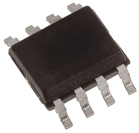
| 产品图片 |
|
| rohs | 符合RoHS无铅 / 符合限制有害物质指令(RoHS)规范要求 |
| 产品系列 | 放大器 IC,运算放大器 - 运放,Texas Instruments OPA343UAMicroAmplifier™ |
| 数据手册 | |
| 产品型号 | OPA343UA |
| 产品目录页面 | |
| 产品种类 | 运算放大器 - 运放 |
| 供应商器件封装 | 8-SOIC |
| 共模抑制比—最小值 | 54 dB |
| 关闭 | No Shutdown |
| 包装 | 管件 |
| 单位重量 | 76 mg |
| 压摆率 | 6 V/µs |
| 商标 | Texas Instruments |
| 增益带宽生成 | 5.5 MHz |
| 增益带宽积 | 5.5MHz |
| 安装类型 | 表面贴装 |
| 安装风格 | SMD/SMT |
| 封装 | Tube |
| 封装/外壳 | 8-SOIC(0.154",3.90mm 宽) |
| 封装/箱体 | SOIC-8 |
| 工作温度 | -40°C ~ 85°C |
| 工作电源电压 | 2.7 V to 5 V |
| 工厂包装数量 | 75 |
| 技术 | CMOS |
| 放大器类型 | Rail to Rail Operational Amplifiers |
| 最大工作温度 | + 85 C |
| 最小工作温度 | - 40 C |
| 标准包装 | 75 |
| 电压-电源,单/双 (±) | 2.5 V ~ 5.5 V |
| 电压-输入失调 | 2mV |
| 电流-电源 | 850µA |
| 电流-输入偏置 | 0.2pA |
| 电流-输出/通道 | 50mA |
| 电源电流 | 0.85 mA |
| 电路数 | 1 |
| 系列 | OPA343 |
| 设计资源 | http://www.digikey.com/product-highlights/cn/zh/texas-instruments-webench-design-center/3176 |
| 转换速度 | 6 V/us |
| 输入偏压电流—最大 | 10 pA |
| 输入参考电压噪声 | 25 nV |
| 输入补偿电压 | 2 mV |
| 输出类型 | Rail to Rail |
| 通道数量 | 1 Channel |


PDF Datasheet 数据手册内容提取
OPA343 OPA2343 OPA4343® OPA2343 OPA4343 OPA4343 www.ti.com SINGLE-SUPPLY, RAIL-TO-RAIL OPERATIONAL AMPLIFIERS Amplifier Series micro ™ FEATURES APPLICATIONS (cid:1) RAIL-TO-RAIL INPUT/OUTPUT (cid:1) DRIVING A/D CONVERTERS (cid:1) MICRO SIZE PACKAGES (cid:1) PCMCIA CARDS (cid:1) WIDE BANDWIDTH: 5.5MHz (cid:1) DATA ACQUISITION (cid:1) HIGH SLEW RATE: 6V/µs (cid:1) AUDIO PROCESSING (cid:1) LOW THD+NOISE: 0.0007% (f = 1kHz) (cid:1) COMMUNICATIONS (cid:1) LOW QUIESCENT CURRENT: 850µA/chan (cid:1) ACTIVE FILTERS (cid:1) SINGLE, DUAL, AND QUAD VERSIONS (cid:1) TEST EQUIPMENT DESCRIPTION The OPA343 series operates on a single supply as low as 2.5V, and input common-mode voltage range extends OPA343 series rail-to-rail CMOS operational amplifiers 500mV beyond the supply rails. Output voltage swings to are designed for low-cost, miniature applications. They within 1mV of the supply rails with a 100kΩ load. They are optimized for low-voltage, single-supply operation. offer excellent dynamic response (BW = 5.5MHz, Rail-to-rail input/output and high-speed operation make SR = 6V/µs), yet quiescent current is only 850µA. Dual them ideal for driving sampling Analog-to-Digital (A/D) and quad designs feature completely independent circuitry converters. They are also well suited for general-purpose for lowest crosstalk and freedom from interaction. and audio applications as well as providing I/V conver- The single (OPA343) packages are the tiny SOT-23-5 sion at the output of Digital-to-Analog (D/A) converters. surface mount and SO-8 surface mount. The dual Single, dual, and quad versions have identical specifica- (OPA2343) comes in the miniature MSOP-8 surface tions for design flexibility. mount and SO-8 surface mount. The quad (OPA4343) packages are the space-saving SSOP-16 surface mount, SO-14 surface mount, and TSSOP-14 surface mount. All OPA343 OPA343 are specified from –40°C to +85°C and operate from NC 1 8 NC –55°C to +125°C. A SPICE macromodel is available for Out 1 5 V+ –In 2 7 V+ design analysis. V– 2 +In 3 6 Output +In 3 4 –In V– 4 5 NC OPA4343 SOT-23-5 OPA4343 Out A 1 16 Out D SO-8 Out A 1 14 Out D –In A 2 15 –In D OPA2343 A D –In A 2 13 –In D +In A 3 14 +In D A D Out A 1 8 V+ +In A 3 12 +In D +V 4 13 –V –In A 2 A 7 Out B V+ 4 11 V– +In B 5 12 +In C B C +In A 3 B 6 –In B +In B 5 10 +In C –In B 6 11 –In C B C –In B 6 9 –In C Out B 7 10 Out C V– 4 5 +In B Out B 7 8 Out C NC 8 9 NC SO-8, MSOP-8 TSSOP-14 SSOP-16 Copyright © 2000, Texas Instruments Incorporated SBOS090A Printed in U.S.A. October, 2000
SPECIFICATIONS: V = 2.7V to 5.5V S ° ° Boldface limits apply over the specified temperature range, T = –40 C to +85 C. V = 5V. A S At T = +25°C, R = 10kΩ connected to V /2 and V = V /2, unless otherwise noted. A L S OUT S OPA343NA, UA OPA2343EA, UA OPA4343EA, UA, NA PARAMETER CONDITION MIN TYP(1) MAX UNITS OFFSET VOLTAGE Input Offset Voltage V V = 5V ±2 ±8 mV OS S vs Temperature dV /dT ±3 µV/°C OS vs Power Supply PSRR V = 2.7V to 5.5V, V = 0V 40 200 µV/V S CM Over Temperature V = 2.7V to 5.5V, V = 0V 200 µV/V S CM Channel Separation, dc 0.2 µV/V INPUT BIAS CURRENT Input Bias Current I ±0.2 ±10 pA B Over Temperature ±60 pA Input Offset Current I ±0.2 ±10 pA OS NOISE Input Voltage Noise, f = 0.1 to 50kHz 8 µVrms Input Voltage Noise Density, f = 1kHz e 25 nV/√Hz n Current Noise Density, f = 1kHz i 3 fA/√Hz n INPUT VOLTAGE RANGE Common-Mode Voltage Range V –0.3 (V+) + 0.3 V CM Common-Mode Rejection Ratio CMRR –0.3V < V < (V+) – 1.8V 74 92 dB CM V = 5V, –0.3V< V < 5.3V 60 75 dB S CM V = 2.7V, –0.3V< V < 3V 54 70 dB S CM INPUT IMPEDANCE Differential 1013 || 3 Ω || pF Common-Mode 1013 || 6 Ω || pF OPEN-LOOP GAIN Open-Loop Voltage Gain A R = 100kΩ, 5mV < V < (V+) – 5mV 100 120 dB OL L O Over Temperature R = 100kΩ, 5mV < V < (V+) – 5mV 100 dB L O R = 10kΩ, 50mV < V < (V+) – 50mV 100 117 dB L O Over Temperature R = 10kΩ, 50mV < V < (V+) – 50mV 100 dB L O R = 2kΩ, 200mV < V < (V+) – 200mV 92 110 dB L O Over Temperature R = 2kΩ, 200mV < V < (V+) – 200mV 92 dB L O FREQUENCY RESPONSE Gain-Bandwidth Product GBW G = 1 5.5 MHz Slew Rate SR V = 5V, G = 1, C = 100pF 6 V/µs S L Settling Time, 0.1% V = 5V, 2V Step, C = 100pF 1 µs S L 0.01% V = 5V, 2V Step, C = 100pF 1.6 µs S L Overload Recovery Time V • G = V 0.2 µs IN S Total Harmonic Distortion + Noise THD+N V = 5V, V = 3Vp-p(2), G = 1, f = 1kHz 0.0007 % S O OUTPUT Voltage Output Swing from Rail(3) R = 100kΩ, A ≥ 100dB 1 5 mV L OL Over Temperature R = 100kΩ, A ≥ 100dB 5 mV L OL R = 10kΩ, A ≥ 100dB 10 50 mV L OL Over Temperature R = 10kΩ, A ≥ 100dB 50 mV L OL R = 2kΩ, A ≥ 92dB 40 200 mV L OL Over Temperature R = 2kΩ, A ≥ 92dB 200 mV L OL Short-Circuit Current I ±50 mA SC Capacitive Load Drive C See Typical Curve LOAD POWER SUPPLY Specified Voltage Range V 2.7 5 V S Operating Voltage Range 2.5 to 5.5 V Quiescent Current (per amplifier) I I = 0, V = +5V 0.85 1.25 mA Q O S Over Temperature I = 0, V = +5V 1.4 mA O S TEMPERATURE RANGE Specified Range –40 +85 °C Operating Range –55 +125 °C Storage Range –65 +150 °C Thermal Resistance θ JA SOT-23-5 Surface Mount 200 °C/W MSOP-8 Surface Mount 150 °C/W SO-8 Surface Mount 150 °C/W SSOP-16 Surface Mount 100 °C/W SO-14 Surface Mount 100 °C/W TSSOP-14 Surface Mount 125 °C/W NOTES: (1) V = +5V. (2) V = 0.25V to 3.25V. (3) Output voltage swings are measured between the output and power supply rails. S OUT 2 OPA343, 2343, 4343 SBOS090A
ABSOLUTE MAXIMUM RATINGS(1) ELECTROSTATIC Supply Voltage...................................................................................7.5V DISCHARGE SENSITIVITY Signal Input Terminals, Voltage(2).....................(V–) –0.5V to (V+) +0.5V Current(2)....................................................10mA This integrated circuit can be damaged by ESD. Burr-Brown Output Short-Circuit(3)..............................................................Continuous Operating Temperature..................................................–55°C to +125°C recommends that all integrated circuits be handled with Storage Temperature.....................................................–65°C to +150°C appropriate precautions. Failure to observe proper handling Junction Temperature......................................................................150°C and installation procedures can cause damage. Lead Temperature (soldering, 10s).................................................300°C NOTES: (1) Stresses above these ratings may cause permanent damage. ESD damage can range from subtle performance degrada- Exposure to absolute maximum conditions for extended periods may de- tion to complete device failure. Precision integrated circuits grade device reliability. (2) Input terminals are diode-clamped to the power may be more susceptible to damage because very small supply rails. Input signals that can swing more than 0.5V beyond the supply rails should be current-limited to 10mA or less. (3) Short-circuit to ground, parametric changes could cause the device not to meet its one amplifier per package. published specifications. PACKAGE/ORDERING INFORMATION PACKAGE SPECIFIED DRAWING TEMPERATURE PACKAGE ORDERING TRANSPORT PRODUCT PACKAGE NUMBER RANGE MARKING NUMBER(1) MEDIA Single OPA343NA 5-Lead SOT-23-5 331 –40°C to +85°C B43 OPA343NA/250 Tape and Reel " " " " " OPA343NA/3K Tape and Reel OPA343UA SO-8 Surface-Mount 182 –40°C to +85°C OPA343UA OPA343UA Rails " " " " " OPA343UA/2K5 Tape and Reel Dual OPA2343EA MSOP-8 Surface-Mount 337 –40°C to +85°C C43 OPA2343EA/250 Tape and Reel " " " " " OPA2343EA/2K5 Tape and Reel OPA2343UA SO-8 Surface-Mount 182 –40°C to +85°C OPA2343UA OPA2343UA Rails " " " " " OPA2343UA/2K5 Tape and Reel Quad OPA4343EA SSOP-16 Surface-Mount 322 –40°C to +85°C OPA4343EA OPA4343EA/250 Tape and Reel " " " " " OPA4343EA/2K5 Tape and Reel OPA4343UA SO-14 Surfac-Mount 235 –40°C to +85°C OPA4343UA OPA4343UA Rails " " " " " OPA4343UA/2K5 Tape and Reel OPA4343NA TSSOP-14 Surface-Mount 357 –40°C to +85°C OPA4343NA OPA4343NA/250 Tape and Reel " " " " " OPA4343NA/2K5 Tape and Reel NOTE: (1) Models with a slash (/) are available only in Tape and Reel in the quantities indicated (e.g., /2K5 indicates 2500 devices per reel). Ordering 2500 pieces of “OPA2343EA/2K5” will get a single 2500 piece Tape and Reel. The information provided herein is believed to be reliable; however, BURR-BROWN assumes no responsibility for inaccuracies or omissions. BURR-BROWN assumes no responsibility for the use of this information, and all use of such information shall be entirely at the user’s own risk. Prices and specifications are subject to change without notice. No patent rights or licenses to any of the circuits described herein are implied or granted to any third party. BURR-BROWN does not authorize or warrant any BURR-BROWN product for use in life support devices and/or systems. OPA343, 2343, 4343 3 SBOS090A
TYPICAL PERFORMANCE CURVES At T = +25°C, V = +5V, and R = 10kΩ connected to V /2, unless otherwise noted. A S L S POWER-SUPPLY and COMMON-MODE OPEN-LOOP GAIN/PHASE vs FREQUENCY REJECTION vs FREQUENCY 160 0 100 140 PSRR 120 –45 80 B) 100 B) Gain (d 80 –90 se (°) MRR (d 60 age 60 Pha R, C 40 Volt 40 –135 PSR V = –0.3VC MtoR (RV+) –1.8V 20 CM 20 0 –180 –20 0 0.1 1 10 100 1k 10k 100k 1M 10M 1 10 100 1k 10k 100k 1M Frequency (Hz) Frequency (Hz) INPUT VOLTAGE AND CURRENT NOISE SPECTRAL DENSITY vs FREQUENCY CHANNEL SEPARATION vs FREQUENCY 10k 1k 140 Current Noise √oise (nVHz) 1010k Voltage Noise 11000 √oise (fAHz) eparation (dB) 113200 N N S Dual and quad devices. Voltage 10 1 Current Channel 110 GQor u =Ba d1to ,m aCell— acshouatrhneendre cclsho.amnbnineal Atio tnos D yield improved rejection. 1 0.1 100 1 10 100 1k 10k 100k 1M 10 100 1k 10k 100k Frequency (Hz) Frequency (Hz) TOTAL HARMONIC DISTORTION + NOISE CLOSED-LOOP OUTPUT IMPEDANCE vs FREQUENCY vs FREQUENCY 0.1 5k R = 600 G = 100 L R = 2k 4k L Ω) 0.01 G = 10 e ( G = 10 %) nc 3k THD+N ( 0.001 G = 1 RL = 600 RL = 10kRL = 2k put Resista 2k G = 1 ut O R = 10k 1k L 0.0001 0 20 100 1k 10k 20k 10 100 1k 10k 100k 1M 10M Frequency (Hz) Frequency (Hz) 4 OPA343, 2343, 4343 SBOS090A
TYPICAL PERFORMANCE CURVES (Cont.) At T = +25°C, V = +5V, and R = 10kΩ connected to V /2, unless otherwise noted. A S L S OPEN-LOOP GAIN AND POWER-SUPPLY REJECTION vs TEMPERATURE COMMON-MODE REJECTION vs TEMPERATURE 130 100 AOL RL = 100kΩ 90 120 , PSRR (dB)OL 111000 RL = 2kΩ RL = 10kΩ CMRR (dB) 876000 A PSRR V = 2.7V to 5V, V = –0.3V to (V+) –1.8V 90 S CM 50 V = 5V, V = –0.3V to 5.3V S CM V = 2.7V, V = –0.3V to 3V S CM 80 40 –75 –50 –25 0 25 50 75 100 125 –75 –50 –25 0 25 50 75 100 125 Temperature (°C) Temperature (°C) QUIESCENT CURRENT vs TEMPERATURE QUIESCENT CURRENT vs SUPPLY VOLTAGE 1100 900 Per Amplifier Per Amplifier 1000 A) A) 850 Current (µ 900 µCurrent ( 800 Quiescent 800 Quiescent 750 700 600 700 –75 –50 –25 0 25 50 75 100 125 2.0 2.5 3.0 3.5 4.0 4.5 5.0 5.5 6.0 Temperature (°C) Supply Voltage (V) SHORT-CIRCUIT CURRENT vs TEMPERATURE SHORT-CIRCUIT CURRENT vs SUPPLY VOLTAGE 100 60 –I 90 SC A) 80 A) m m –ISC nt ( 70 nt ( 50 urre 60 urre Circuit C 5400 +ISC Circuit C 40 +ISC ort- 30 ort- Sh 20 Sh 10 0 30 –75 –50 –25 0 25 50 75 100 125 2.0 2.5 3.0 3.5 4.0 4.5 5.0 5.5 6.0 Temperature (°C) Supply Voltage (V) OPA343, 2343, 4343 5 SBOS090A
TYPICAL PERFORMANCE CURVES (Cont.) At T = +25°C, V = +5V, and R = 10kΩ connected to V /2, unless otherwise noted. A S L S INPUT BIAS CURRENT INPUT BIAS CURRENT vs TEMPERATURE vs INPUT COMMON-MODE VOLTAGE 1000 1.0 0.8 0.6 Input Bias Current (pA) 110100 Input Bias Current (pA) –––00000.....042246 –0.8 0.1 –1.0 –60 –40 –20 0 20 40 60 80 100 –1 0 1 2 3 4 5 6 Temperature (°C) Common-Mode Voltage (V) OUTPUT VOLTAGE SWING vs OUTPUT CURRENT MAXIMUM OUTPUT VOLTAGE vs FREQUENCY 5 6 V = 5.5V S Maximum output +125°C +25°C –55°C 5 voltage without 4 slew rate-induced p) distortion. ge (V) 3 e (Vp- 4 a g Volt olta 3 VS = 2.7V Output 2 utput V 2 O 1 +125°C +25°C –55°C 1 0 0 0 ±10 ±20 ±30 ±40 ±50 ±60 ±70 ±80 ±90 ±100 100k 1M 10M Output Current (mA) Frequency (Hz) OFFSET VOLTAGE OFFSET VOLTAGE DRIFT PRODUCTION DISTRIBUTION PRODUCTION DISTRIBUTION 30 25 Typical production Typical production distribution of distribution of 25 packaged units. 20 packaged units. %) %) s ( 20 s ( er er plifi plifi 15 m 15 m A A of of 10 nt 10 nt e e c c er er P P 5 5 0 0 –8 –7 –6 –5 –4 –3 –2 –1 0 1 2 3 4 5 6 7 8 0 1 2 3 4 5 6 7 8 9 10 11 12 13 14 Offset Voltage Drift (µV/°C) Offset Voltage (mV) 6 OPA343, 2343, 4343 SBOS090A
TYPICAL PERFORMANCE CURVES (Cont.) At T = +25°C, V = +5V, and R = 10kΩ connected to V /2, unless otherwise noted. A S L S SMALL-SIGNAL STEP RESPONSE LARGE-SIGNAL STEP RESPONSE CL = 100pF CL = 100pF 50mV/div 1V/div 1µs/div 1µs/div SMALL-SIGNAL OVERSHOOT vs LOAD CAPACITANCE SETTLING TIME vs CLOSED-LOOP GAIN 60 100 50 G = –1 0.01% %) 40 G = +1 µs) 10 ot ( me ( Oversho 3200 G = ±5 ettling Ti 1 0.1% S 10 See text for reducing overshoot. 0 0.1 100 1000 10k 1 10 100 1000 Load Capacitance (pF) Closed-Loop Gain (V/V) OPA343, 2343, 4343 7 SBOS090A
APPLICATIONS INFORMATION OPERATING VOLTAGE OPA343 series op amps are fully specified from +2.7V to OPA343 series op amps are fabricated on a state-of-the-art +5V. However, supply voltage may range from +2.5V to 0.6 micron CMOS process. They are unity-gain stable and +5.5V. Parameters are guaranteed over the specified supply suitable for a wide range of general-purpose applications. range—a unique feature of the OPA343 series. In addition, Rail-to-rail input/output make them ideal for driving sam- many specifications apply from –40°C to +85°C. Most pling A/D converters. In addition, excellent ac performance behavior remains virtually unchanged throughout the full makes them well-suited for audio applications. The class AB operating voltage range. Parameters which vary signifi- output stage is capable of driving 600Ω loads connected to cantly with operating voltages or temperature are shown in any point between V+ and ground. the Typical Performance Curves. Rail-to-rail input and output swing significantly increases dynamic range, especially in low-supply applications. Fig- RAIL-TO-RAIL INPUT ure 1 shows the input and output waveforms for the OPA343 in unity-gain configuration. Operation is from a The input common-mode voltage range of the OPA343 single +5V supply with a 10kΩ load connected to V /2. series extends 500mV beyond the supply rails. This is S The input is a 5Vp-p sinusoid. Output voltage is approxi- achieved with a complementary input stage—an N-channel mately 4.98Vp-p. input differential pair in parallel with a P-channel differen- tial pair, as shown in Figure 2. The N-channel pair is active Power-supply pins should be bypassed with 0.01µF ceramic for input voltages close to the positive rail, typically (V+) capacitors. – 1.3V to 500mV above the positive supply. The P-channel pair is on for inputs from 500mV below the negative supply to approximately (V+) – 1.3V. V = +5, G = +1, R = 10kΩ S L There is a small transition region, typically (V+) – 1.5V to (V+) – 1.1V, in which both input pairs are on. This 400mV 5 transition region can vary ±300mV with process variation. VIN Thus, the transition region (both stages on) can range from (V+) – 1.8V to (V+) – 1.4V on the low end, up to (V+) v V/di – 1.2V to (V+) – 0.8V on the high end. Within the 400mV 2 transition region PSRR, CMRR, offset voltage, offset drift, 5 and THD may be degraded compared to operation outside VOUT this region. A double-folded cascode adds the signal from the two input 0 pairs and presents a differential signal to the class AB output stage. Normally, input bias current is approximately 200fA, FIGURE 1. Rail-to-Rail Input and Output. however, input voltages exceeding the power supplies by V+ Reference Current VIN+ VIN– VBIAS1 Class AB Control V O Circuitry V BIAS2 V– (Ground) FIGURE 2. Simplified Schematic. 8 OPA343, 2343, 4343 SBOS090A
more than 500mV can cause excessive current to flow in or capacitive load reacts with the op amp’s output resistance, out of the input pins. Momentary voltages greater than along with any additional load resistance, to create a pole in 500mV beyond the power supply can be tolerated if the the small-signal response which degrades the phase margin. current on the input pins is limited to 10mA. This is easily In unity gain, OPA343 series op amps perform well, with a accomplished with an input resistor, as shown in Figure 3. pure capacitive load up to approximately 1000pF. Increasing Many input signals are inherently current-limited to less gain enhances the amplifier’s ability to drive more capaci- than 10mA, therefore, a limiting resistor is not required. tance. See the typical performance curve “Small-Signal Overshoot vs Capacitive Load.” One method of improving capacitive load drive in the unity gain configuration is to insert a 10Ω to 20Ω resistor in series with the output, as shown in Figure 4. This significantly V+ reduces ringing with large capacitive loads. However, if I OVERLOAD there is a resistive load in parallel with the capacitive load, 10mA max OPAx343 VOUT RS creates a voltage divider. This introduces a dc error at the VIN output and slightly reduces output swing. This error may be 5kΩ insignificant. For instance, with R = 10kΩ and R = 20Ω, L S there is only about a 0.2% error at the output. FIGURE 3. Input Current Protection for Voltages Exceeding DRIVING A/D CONVERTERS the Supply Voltage. OPA343 series op amps are optimized for driving medium speed (up to 100kHz) sampling A/D converters. However, RAIL-TO-RAIL OUTPUT they also offer excellent performance for higher-speed A class AB output stage with common-source transistors is converters. The OPA343 series provides an effective means used to achieve rail-to-rail output. For light resistive loads of buffering the A/D’s input capacitance and resulting (>50kΩ), the output voltage is typically a few millivolts charge injection while providing signal gain. For applica- from the supply rails. With moderate resistive loads (2kΩ to tions requiring high accuracy, the OPA340 series is recom- 50kΩ), the output can swing to within a few tens of milli- mended. volts from the supply rails and maintain high open-loop Figures 5 and 6 show the OPA343 driving an ADS7816. gain. See the typical performanc curve “Output Voltage The ADS7816 is a 12-bit, micro-power sampling converter Swing vs Output Current.” in the tiny MSOP-8 package. When used with the minia- ture package options of the OPA343 series, the combina- CAPACITIVE LOAD AND STABILITY tion is ideal for space-limited and low-power applications. For further information consult the ADS7816 data sheet. OPA343 series op amps can drive a wide range of capacitive loads. However, all op amps under certain conditions may With the OPA343 in a noninverting configuration, an RC become unstable. Op amp configuration, gain, and load network at the amplifier’s output can be used to filter high value are just a few of the factors to consider when determin- frequency noise in the signal (see Figure 5). In the invert- ing stability. An op amp in unity gain configuration is the ing configuration, filtering may be accomplished with a most susceptible to the effects of capacitive load. The capacitor across the feedback resistor (see Figure 6). V+ R S OPAx343 VOUT V 10Ω to IN 20Ω RL CL FIGURE 4. Series Resistor in Unity-Gain Configuration Improves Capacitive Load Drive. OPA343, 2343, 4343 9 SBOS090A
+5V For improved accuracy use OPA340. 0.1µF 0.1µF 8 V+ 1 VREF 7 500Ω +In ADS7816 DCLOCK 6 Serial OPA343 D VIN 2–In 12-Bit A/D CS/SHODUNT 5 Interface 3300pF 3 GND 4 V = 0V to 5V for IN 0V to 5V output. NOTE: A/D Input = 0 to V REF RC network filters high frequency noise. FIGURE 5. OPA343 in Noninverting Configuration Driving ADS7816. +5V 330pF For improved accuracy use OPA340. 0.1µF 0.1µF 5kΩ 5kΩ V IN 8 V+ 1 VREF 7 DCLOCK +In ADS7816 6 Serial OPA343 D 2 12-Bit A/D OUT 5 Interface –In CS/SHDN 3 GND 4 VIN = 0V to –5V for 0V to 5V output. NOTE: A/D Input = 0 to VREF FIGURE 6. OPA343 in Inverting Configuration Driving ADS7816. +5V Filters 160Hz to 2.4kHz 10MΩ VIN 1/2 243kΩ 1.74MΩ 200pF 10MΩ OPA2343 1/2 47pF OPA2343 R L 220pF FIGURE 7. Speech Bandpass Filter. <1pF (prevents gain peaking) 10MΩ +V λ OPA343 V O FIGURE 8. Transimpedance Amplifier. 10 OPA343, 2343, 4343 SBOS090A
PACKAGE OPTION ADDENDUM www.ti.com 6-Feb-2020 PACKAGING INFORMATION Orderable Device Status Package Type Package Pins Package Eco Plan Lead/Ball Finish MSL Peak Temp Op Temp (°C) Device Marking Samples (1) Drawing Qty (2) (6) (3) (4/5) OPA2343EA/250 ACTIVE VSSOP DGK 8 250 Green (RoHS NIPDAUAG Level-2-260C-1 YEAR -40 to 85 C43 & no Sb/Br) OPA2343EA/250G4 ACTIVE VSSOP DGK 8 250 Green (RoHS NIPDAUAG Level-2-260C-1 YEAR -40 to 85 C43 & no Sb/Br) OPA2343EA/2K5 ACTIVE VSSOP DGK 8 2500 Green (RoHS NIPDAUAG Level-2-260C-1 YEAR -40 to 85 C43 & no Sb/Br) OPA2343EA/2K5G4 ACTIVE VSSOP DGK 8 2500 Green (RoHS NIPDAUAG Level-2-260C-1 YEAR -40 to 85 C43 & no Sb/Br) OPA2343UA ACTIVE SOIC D 8 75 Green (RoHS NIPDAU Level-2-260C-1 YEAR -40 to 85 OPA & no Sb/Br) 2343UA OPA2343UA/2K5 ACTIVE SOIC D 8 2500 Green (RoHS NIPDAU Level-2-260C-1 YEAR -40 to 85 OPA & no Sb/Br) 2343UA OPA2343UA/2K5G4 ACTIVE SOIC D 8 2500 Green (RoHS NIPDAU Level-2-260C-1 YEAR -40 to 85 OPA & no Sb/Br) 2343UA OPA343NA/250 ACTIVE SOT-23 DBV 5 250 Green (RoHS NIPDAU Level-1-260C-UNLIM -40 to 85 B43 & no Sb/Br) OPA343NA/250G4 ACTIVE SOT-23 DBV 5 250 Green (RoHS NIPDAU Level-1-260C-UNLIM -40 to 85 B43 & no Sb/Br) OPA343NA/3K ACTIVE SOT-23 DBV 5 3000 Green (RoHS NIPDAU Level-1-260C-UNLIM -40 to 85 B43 & no Sb/Br) OPA343NA/3KG4 ACTIVE SOT-23 DBV 5 3000 Green (RoHS NIPDAU Level-1-260C-UNLIM -40 to 85 B43 & no Sb/Br) OPA343UA ACTIVE SOIC D 8 75 Green (RoHS NIPDAU Level-2-260C-1 YEAR -40 to 85 OPA & no Sb/Br) 343UA OPA343UA/2K5 ACTIVE SOIC D 8 2500 Green (RoHS NIPDAU Level-2-260C-1 YEAR -40 to 85 OPA & no Sb/Br) 343UA OPA343UA/2K5G4 ACTIVE SOIC D 8 2500 Green (RoHS NIPDAU Level-2-260C-1 YEAR -40 to 85 OPA & no Sb/Br) 343UA OPA4343EA/250 ACTIVE SSOP DBQ 16 250 Green (RoHS NIPDAU Level-2-260C-1 YEAR -40 to 85 OPA & no Sb/Br) 4343EA OPA4343EA/2K5 ACTIVE SSOP DBQ 16 2500 Green (RoHS NIPDAU Level-2-260C-1 YEAR -40 to 85 OPA & no Sb/Br) 4343EA OPA4343NA/250 ACTIVE TSSOP PW 14 250 Green (RoHS NIPDAU Level-2-260C-1 YEAR -40 to 85 OPA & no Sb/Br) 4343NA Addendum-Page 1
PACKAGE OPTION ADDENDUM www.ti.com 6-Feb-2020 Orderable Device Status Package Type Package Pins Package Eco Plan Lead/Ball Finish MSL Peak Temp Op Temp (°C) Device Marking Samples (1) Drawing Qty (2) (6) (3) (4/5) OPA4343NA/2K5 ACTIVE TSSOP PW 14 2500 Green (RoHS NIPDAU Level-2-260C-1 YEAR -40 to 85 OPA & no Sb/Br) 4343NA OPA4343UA ACTIVE SOIC D 14 50 Green (RoHS NIPDAU Level-2-260C-1 YEAR -40 to 85 OPA4343UA & no Sb/Br) OPA4343UA/2K5 ACTIVE SOIC D 14 2500 Pb-Free NIPDAU Level-1-260C-UNLIM -40 to 85 OPA4343UA (RoHS) (1) The marketing status values are defined as follows: ACTIVE: Product device recommended for new designs. LIFEBUY: TI has announced that the device will be discontinued, and a lifetime-buy period is in effect. NRND: Not recommended for new designs. Device is in production to support existing customers, but TI does not recommend using this part in a new design. PREVIEW: Device has been announced but is not in production. Samples may or may not be available. OBSOLETE: TI has discontinued the production of the device. (2) RoHS: TI defines "RoHS" to mean semiconductor products that are compliant with the current EU RoHS requirements for all 10 RoHS substances, including the requirement that RoHS substance do not exceed 0.1% by weight in homogeneous materials. Where designed to be soldered at high temperatures, "RoHS" products are suitable for use in specified lead-free processes. TI may reference these types of products as "Pb-Free". RoHS Exempt: TI defines "RoHS Exempt" to mean products that contain lead but are compliant with EU RoHS pursuant to a specific EU RoHS exemption. Green: TI defines "Green" to mean the content of Chlorine (Cl) and Bromine (Br) based flame retardants meet JS709B low halogen requirements of <=1000ppm threshold. Antimony trioxide based flame retardants must also meet the <=1000ppm threshold requirement. (3) MSL, Peak Temp. - The Moisture Sensitivity Level rating according to the JEDEC industry standard classifications, and peak solder temperature. (4) There may be additional marking, which relates to the logo, the lot trace code information, or the environmental category on the device. (5) Multiple Device Markings will be inside parentheses. Only one Device Marking contained in parentheses and separated by a "~" will appear on a device. If a line is indented then it is a continuation of the previous line and the two combined represent the entire Device Marking for that device. (6) Lead/Ball Finish - Orderable Devices may have multiple material finish options. Finish options are separated by a vertical ruled line. Lead/Ball Finish values may wrap to two lines if the finish value exceeds the maximum column width. Important Information and Disclaimer:The information provided on this page represents TI's knowledge and belief as of the date that it is provided. TI bases its knowledge and belief on information provided by third parties, and makes no representation or warranty as to the accuracy of such information. Efforts are underway to better integrate information from third parties. TI has taken and continues to take reasonable steps to provide representative and accurate information but may not have conducted destructive testing or chemical analysis on incoming materials and chemicals. TI and TI suppliers consider certain information to be proprietary, and thus CAS numbers and other limited information may not be available for release. In no event shall TI's liability arising out of such information exceed the total purchase price of the TI part(s) at issue in this document sold by TI to Customer on an annual basis. Addendum-Page 2
PACKAGE OPTION ADDENDUM www.ti.com 6-Feb-2020 Addendum-Page 3
PACKAGE MATERIALS INFORMATION www.ti.com 16-Jul-2020 TAPE AND REEL INFORMATION *Alldimensionsarenominal Device Package Package Pins SPQ Reel Reel A0 B0 K0 P1 W Pin1 Type Drawing Diameter Width (mm) (mm) (mm) (mm) (mm) Quadrant (mm) W1(mm) OPA2343EA/250 VSSOP DGK 8 250 330.0 12.4 5.3 3.4 1.4 8.0 12.0 Q1 OPA2343EA/250 VSSOP DGK 8 250 330.0 12.4 5.3 3.4 1.4 8.0 12.0 Q1 OPA2343EA/2K5 VSSOP DGK 8 2500 330.0 12.4 5.3 3.4 1.4 8.0 12.0 Q1 OPA2343EA/2K5 VSSOP DGK 8 2500 330.0 12.4 5.3 3.4 1.4 8.0 12.0 Q1 OPA2343UA/2K5 SOIC D 8 2500 330.0 12.4 6.4 5.2 2.1 8.0 12.0 Q1 OPA343NA/250 SOT-23 DBV 5 250 178.0 9.0 3.23 3.17 1.37 4.0 8.0 Q3 OPA343NA/3K SOT-23 DBV 5 3000 178.0 9.0 3.23 3.17 1.37 4.0 8.0 Q3 OPA343UA/2K5 SOIC D 8 2500 330.0 12.4 6.4 5.2 2.1 8.0 12.0 Q1 OPA4343EA/250 SSOP DBQ 16 250 180.0 12.4 6.4 5.2 2.1 8.0 12.0 Q1 OPA4343EA/2K5 SSOP DBQ 16 2500 330.0 12.4 6.4 5.2 2.1 8.0 12.0 Q1 OPA4343NA/250 TSSOP PW 14 250 180.0 12.4 6.9 5.6 1.6 8.0 12.0 Q1 OPA4343NA/2K5 TSSOP PW 14 2500 330.0 12.4 6.9 5.6 1.6 8.0 12.0 Q1 OPA4343UA/2K5 SOIC D 14 2500 330.0 16.4 6.5 9.0 2.1 8.0 16.0 Q1 PackMaterials-Page1
PACKAGE MATERIALS INFORMATION www.ti.com 16-Jul-2020 *Alldimensionsarenominal Device PackageType PackageDrawing Pins SPQ Length(mm) Width(mm) Height(mm) OPA2343EA/250 VSSOP DGK 8 250 366.0 364.0 50.0 OPA2343EA/250 VSSOP DGK 8 250 366.0 364.0 50.0 OPA2343EA/2K5 VSSOP DGK 8 2500 366.0 364.0 50.0 OPA2343EA/2K5 VSSOP DGK 8 2500 366.0 364.0 50.0 OPA2343UA/2K5 SOIC D 8 2500 367.0 367.0 35.0 OPA343NA/250 SOT-23 DBV 5 250 180.0 180.0 18.0 OPA343NA/3K SOT-23 DBV 5 3000 180.0 180.0 18.0 OPA343UA/2K5 SOIC D 8 2500 367.0 367.0 35.0 OPA4343EA/250 SSOP DBQ 16 250 210.0 185.0 35.0 OPA4343EA/2K5 SSOP DBQ 16 2500 367.0 367.0 35.0 OPA4343NA/250 TSSOP PW 14 250 210.0 185.0 35.0 OPA4343NA/2K5 TSSOP PW 14 2500 367.0 367.0 35.0 OPA4343UA/2K5 SOIC D 14 2500 367.0 367.0 38.0 PackMaterials-Page2
IMPORTANTNOTICEANDDISCLAIMER TI PROVIDES TECHNICAL AND RELIABILITY DATA (INCLUDING DATASHEETS), DESIGN RESOURCES (INCLUDING REFERENCE DESIGNS), APPLICATION OR OTHER DESIGN ADVICE, WEB TOOLS, SAFETY INFORMATION, AND OTHER RESOURCES “AS IS” AND WITH ALL FAULTS, AND DISCLAIMS ALL WARRANTIES, EXPRESS AND IMPLIED, INCLUDING WITHOUT LIMITATION ANY IMPLIED WARRANTIES OF MERCHANTABILITY, FITNESS FOR A PARTICULAR PURPOSE OR NON-INFRINGEMENT OF THIRD PARTY INTELLECTUAL PROPERTY RIGHTS. These resources are intended for skilled developers designing with TI products. You are solely responsible for (1) selecting the appropriate TI products for your application, (2) designing, validating and testing your application, and (3) ensuring your application meets applicable standards, and any other safety, security, or other requirements. These resources are subject to change without notice. TI grants you permission to use these resources only for development of an application that uses the TI products described in the resource. Other reproduction and display of these resources is prohibited. No license is granted to any other TI intellectual property right or to any third party intellectual property right. TI disclaims responsibility for, and you will fully indemnify TI and its representatives against, any claims, damages, costs, losses, and liabilities arising out of your use of these resources. TI’s products are provided subject to TI’s Terms of Sale (www.ti.com/legal/termsofsale.html) or other applicable terms available either on ti.com or provided in conjunction with such TI products. TI’s provision of these resources does not expand or otherwise alter TI’s applicable warranties or warranty disclaimers for TI products. Mailing Address: Texas Instruments, Post Office Box 655303, Dallas, Texas 75265 Copyright © 2020, Texas Instruments Incorporated