ICGOO在线商城 > 集成电路(IC) > 线性 - 放大器 - 仪表,运算放大器,缓冲器放大器 > OP284FS
 Datasheet下载
- 型号: OP284FS
- 制造商: Analog
- 库位|库存: xxxx|xxxx
- 要求:
| 数量阶梯 | 香港交货 | 国内含税 |
| +xxxx | $xxxx | ¥xxxx |
查看当月历史价格
查看今年历史价格
OP284FS产品简介:
ICGOO电子元器件商城为您提供OP284FS由Analog设计生产,在icgoo商城现货销售,并且可以通过原厂、代理商等渠道进行代购。 OP284FS价格参考¥62.06-¥69.82。AnalogOP284FS封装/规格:线性 - 放大器 - 仪表,运算放大器,缓冲器放大器, 通用 放大器 2 电路 满摆幅 8-SOIC。您可以下载OP284FS参考资料、Datasheet数据手册功能说明书,资料中有OP284FS 详细功能的应用电路图电压和使用方法及教程。
Analog Devices Inc. 的OP284FS是一款高性能的双通道运算放大器,广泛应用于各种精密测量和信号处理领域。其主要应用场景包括:

1. 工业自动化与控制:在工业控制系统中,OP284FS用于传感器信号调理,如温度、压力、位移等传感器的信号放大与滤波。它能够提供高精度和低噪声的信号处理,确保控制系统稳定可靠。

2. 医疗设备:在医疗仪器中,OP284FS可用于心电图(ECG)、脑电图(EEG)等生物电信号的放大。其低输入偏置电流和高共模抑制比(CMRR)特性,使得它可以精确地捕捉微弱的生理信号,同时减少干扰。

3. 测试与测量仪器:OP284FS适用于高精度的电压表、电流表等测量仪器。其优异的线性度和稳定性,保证了测量结果的准确性。此外,它还可以用于示波器前端的信号放大,提高信号保真度。

4. 音频处理:在高端音频设备中,OP284FS用于前置放大器或缓冲器,以提升音频信号的质量。其低失真和宽频带特性,能够还原更纯净的声音,适合专业音频设备和家庭影院系统。

5. 通信设备:在无线通信系统中,OP284FS可以用于射频(RF)信号的中频(IF)放大。它具有良好的温度稳定性和低噪声特性,有助于提高通信系统的信噪比,增强信号传输质量。

6. 汽车电子:在汽车传感器和控制系统中,OP284FS用于处理来自各种传感器(如氧传感器、加速度计等)的信号。其高可靠性设计,使其能够在恶劣的车载环境中长期稳定工作。

7. 数据采集系统:OP284FS可用于多通道数据采集系统中的信号调理模块。它能够同时处理多个传感器的信号,确保数据采集的同步性和准确性,适用于环境监测、振动分析等领域。

总之,OP284FS凭借其卓越的性能和可靠性,在多个行业和应用领域中发挥着重要作用,特别是在需要高精度、低噪声和高稳定性的场合。
| 参数 | 数值 |
| -3db带宽 | - |
| 产品目录 | 集成电路 (IC)半导体 |
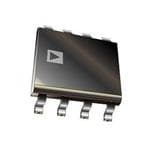
| 描述 | IC OPAMP GP 4.25MHZ RRO 8SOIC运算放大器 - 运放 PREC RRIO 4MHz IC 65uV |
| 产品分类 | Linear - Amplifiers - Instrumentation, OP Amps, Buffer Amps集成电路 - IC |
| 品牌 | Analog Devices Inc |
| 产品手册 | |
| 产品图片 |
|
| rohs | 否不符合限制有害物质指令(RoHS)规范要求 |
| 产品系列 | 放大器 IC,运算放大器 - 运放,Analog Devices OP284FS- |
| 数据手册 | |
| 产品型号 | OP284FS |
| 产品培训模块 | http://www.digikey.cn/PTM/IndividualPTM.page?site=cn&lang=zhs&ptm=30008http://www.digikey.cn/PTM/IndividualPTM.page?site=cn&lang=zhs&ptm=26202 |
| 产品种类 | 运算放大器 - 运放 |
| 供应商器件封装 | 8-SOIC |
| 共模抑制比—最小值 | 60 dB |
| 关闭 | No Shutdown |
| 包装 | 管件 |
| 压摆率 | 4 V/µs |
| 双重电源电压 | +/- 3 V, +/- 5 V, +/- 9 V, +/- 12 V, +/- 15 V |
| 商标 | Analog Devices |
| 增益带宽生成 | 3.25 MHz |
| 增益带宽积 | 4.25MHz |
| 安装类型 | 表面贴装 |
| 安装风格 | SMD/SMT |
| 封装 | Tube |
| 封装/外壳 | 8-SOIC(0.154",3.90mm 宽) |
| 封装/箱体 | SOIC-8 |
| 工作温度 | -40°C ~ 85°C |
| 工作电源电压 | 3 V to 36 V |
| 工厂包装数量 | 98 |
| 技术 | Bipolar |
| 放大器类型 | 通用 |
| 最大双重电源电压 | +/- 18 V |
| 最大工作温度 | + 125 C |
| 最小双重电源电压 | +/- 1.5 V |
| 最小工作温度 | - 40 C |
| 标准包装 | 98 |
| 电压-电源,单/双 (±) | 3 V ~ 36 V, ±1.5 V ~ 18 V |
| 电压-输入失调 | 175µV |
| 电流-电源 | 2.25mA |
| 电流-输入偏置 | 80nA |
| 电流-输出/通道 | 10mA |
| 电源电流 | 2.9 mA |
| 电路数 | 2 |
| 系列 | OP284 |
| 视频文件 | http://www.digikey.cn/classic/video.aspx?PlayerID=1364138032001&width=640&height=505&videoID=2245193153001http://www.digikey.cn/classic/video.aspx?PlayerID=1364138032001&width=640&height=505&videoID=2245193159001 |
| 转换速度 | 4 V/us |
| 输入偏压电流—最大 | 450 nA |
| 输入补偿电压 | 65 uV |
| 输出电流 | 6.5 mA |
| 输出类型 | 满摆幅 |
| 通道数量 | 2 Channel |


- 商务部:美国ITC正式对集成电路等产品启动337调查
- 曝三星4nm工艺存在良率问题 高通将骁龙8 Gen1或转产台积电
- 太阳诱电将投资9.5亿元在常州建新厂生产MLCC 预计2023年完工
- 英特尔发布欧洲新工厂建设计划 深化IDM 2.0 战略
- 台积电先进制程称霸业界 有大客户加持明年业绩稳了
- 达到5530亿美元!SIA预计今年全球半导体销售额将创下新高
- 英特尔拟将自动驾驶子公司Mobileye上市 估值或超500亿美元
- 三星加码芯片和SET,合并消费电子和移动部门,撤换高东真等 CEO
- 三星电子宣布重大人事变动 还合并消费电子和移动部门
- 海关总署:前11个月进口集成电路产品价值2.52万亿元 增长14.8%


PDF Datasheet 数据手册内容提取
Precision Rail-to-Rail Input and Output Operational Amplifiers OP184/OP284/OP484 FEATURES PIN CONFIGURATIONS Single-supply operation Wide bandwidth: 4 MHz DNC 1 OP184 8 NC Low offset voltage: 65 μV –IN A 2 7 V+ Unity-gain stable – +IN A 3 6 OUT A High slew rate: 4.0 V/μs + V– 4 TOP VIEW 5 DNC Low noise: 3.9 nV/√Hz (Not to Scale) APPLICATIONS N12..O NDTCNE CS= =N ODO C ONONNT ECCOTNNECT 00293-001 Battery-powered instrumentation Figure 1. 8-Lead SOIC (S-Suffix) Power supply control and protection Telecommunications OP284 OUT A 1 8 V+ DAC output amplifier ADC input buffer –IN A 2 7 OUT B +IN A 3 6 –IN B GThEeN OEPR18A4L/O DP2E8S4C/ORPI4P8T4I aOreN s ingle, dual, and quad single-supply, V– 4 (NToOt Pto V SIEcaWle) 5 +IN B00293-002 Figure 2. 8-Lead PDIP (P-Suffix) 4 MHz bandwidth amplifiers featuring rail-to-rail inputs and 8-Lead SOIC (S-Suffix) outputs. They are guaranteed to operate from 3 V to 36 V (or ±1.5 V to ±18 V). OUT A 1 14 OUT D These amplifiers are superb for single-supply applications requiring –IN A 2 13 –IN D both ac and precision dc performance. The combination of wide +IN A 3 12 +IN D OP484 bandwidth, low noise, and precision makes the OP184/OP284/ V+ 4 TOP VIEW 11 V– OP484 useful in a wide variety of applications, including filters +IN B 5 (Not to Scale) 10 +IN C and instrumentation. –IN B 6 9 –IN C Other applications for these amplifiers include portable telecom- OUT B 7 8 OUT C 00293-003 munications equipment, power supply control and protection, Figure 3. 14-Lead PDIP (P-Suffix) and use as amplifiers or buffers for transducers with wide output 14-Lead Narrow-Body SOIC (S-Suffix) ranges. Sensors requiring a rail-to-rail input amplifier include Hall effect, piezoelectric, and resistive transducers. The ability to swing rail-to-rail at both the input and output enables designers to build multistage filters in single-supply systems and to maintain high signal-to-noise ratios. The OP184/OP284/OP484 are specified over the hot extended industrial temperature range of −40°C to +125°C. The single OP184 is available in 8-lead SOIC surface mount packages. The dual OP284 is available in 8-lead PDIP and SOIC surface mount packages. The quad OP484 is available in 14-lead PDIP and 14-lead, narrow-body SOIC packages. Table 1. Low Noise Op Amps Voltage Noise 0.9 nV 1.1 nV 1.8 nV 2.8 nV 3.2 nV 3.8 nV 3.9 nV Single AD797 AD8597 ADA4004-1 AD8675/ADA4075-2 OP27 AD8671 OP184 Dual AD8599 ADA4004-2 AD8676 OP270 AD8672 OP284 Quad ADA4004-4 OP470 AD8674 OP484 Rev. J Information furnished by Analog Devices is believed to be accurate and reliable. However, no responsibility is assumed by Analog Devices for its use, nor for any infringements of patents or other One Technology Way, P.O. Box 9106, Norwood, MA 02062-9106, U.S.A. rights of third parties that may result from its use. Specifications subject to change without notice. No license is granted by implication or otherwise under any patent or patent rights of Analog Devices. Tel: 781.329.4700 www.analog.com Trademarks and registered trademarks are the property of their respective owners. Fax: 781.461.3113 ©1996–2011 Analog Devices, Inc. All rights reserved.
OP184/OP284/OP484 TABLE OF CONTENTS Features .............................................................................................. 1 Output Phase Reversal ............................................................... 15 Applications ....................................................................................... 1 Designing Low Noise Circuits in Single-Supply Applications General Description ......................................................................... 1 ....................................................................................................... 15 Pin Configurations ........................................................................... 1 Overdrive Recovery ................................................................... 16 Revision History ............................................................................... 2 Single-Supply, 3 V Instrumentation Amplifier ...................... 16 Specifications ..................................................................................... 3 2.5 V Reference from a 3 V Supply .......................................... 17 Electrical Characteristics ............................................................. 3 5 V Only, 12-Bit DAC Swings Rail-to-Rail ............................. 17 Absolute Maximum Ratings ............................................................ 6 High-Side Current Monitor ...................................................... 18 Thermal Resistance ...................................................................... 6 Capacitive Load Drive Capability ............................................ 18 ESD Caution .................................................................................. 6 Low Dropout Regulator with Current Limiting ..................... 19 Typical Performance Characteristics ............................................. 7 3 V, 50 Hz/60 Hz Active Notch Filter with False Ground ..... 20 Applications Information .............................................................. 14 Outline Dimensions ....................................................................... 21 Functional Description .............................................................. 14 Ordering Guide .......................................................................... 23 Input Overvoltage Protection ................................................... 14 REVISION HISTORY 4/11—Rev. I to Rev J 4/06—Rev. C to Rev. D Change to Figure 27 ....................................................................... 10 Changes to Table 1 ............................................................................. 3 Changes to Table 2 ............................................................................. 4 10/10—Rev. H to Rev I Changes to Table 3 ............................................................................. 5 Change to Output Characteristics, Output Voltage High Deleted Reference to 1993 System Applications Guide .............. 15 Parameter, Table 2 ............................................................................. 3 3/06—Rev. B to Rev. C Change to Output Characteristics, Output Voltage High Parameter, Table 3 ............................................................................. 4 Changes to Figure 1 Caption............................................................ 1 Changes to Table 1 ............................................................................. 3 7/10—Rev. G to Rev. H Changes to Table 2 ............................................................................. 4 Added Table 1 .................................................................................... 1 Changes to Table 3 ............................................................................. 5 Changes to Table 4 ............................................................................. 6 2/09—Rev. F to Rev. G Changes to Figure 5 through Figure 9 ............................................ 7 Change to Large Signal Voltage Gain, Table 3 .............................. 5 Changes to Functional Description Section ............................... 14 Updated Outline Dimensions ....................................................... 21 Deleted SPICE Macro Model ........................................................ 21 Changes to Ordering Guide .......................................................... 22 Updated Outline Dimensions ....................................................... 21 Changes to Ordering Guide .......................................................... 22 9/08—Rev. E to Rev. F 9/02—Rev. A to Rev. B Changes to General Description .................................................... 1 Changes to Figure 4 .......................................................................... 6 Changes to Pin Configurations ....................................................... 1 Changes to Low Dropout Regulator with Current Limiting .... 20 Changes to Specifications, Input Bias Current Maximum .......... 2 Changes to Ordering Guide ............................................................. 5 7/08—Rev. D to Rev. E Updated Outline Dimensions ....................................................... 19 Changes to Figure 1 .......................................................................... 1 6/02—Rev. 0 to Rev. A Changes to Figure 12 ........................................................................ 8 Changes to Figure 36 and Figure 37 ............................................. 12 10/96—Revision 0: Initial Version Changes to Designing Low Noise Circuits in Single-Supply Applications Section ....................................................................... 15 Updated Outline Dimensions ....................................................... 21 Changes to Ordering Guide .......................................................... 22 Rev. J | Page 2 of 24
OP184/OP284/OP484 SPECIFICATIONS ELECTRICAL CHARACTERISTICS V = 5.0 V, V = 2.5 V, T = 25°C, unless otherwise noted. S CM A Table 2. Parameter Symbol Conditions Min Typ Max Unit INPUT CHARACTERISTICS Offset Voltage, OP184/OP284E Grade1 V 65 μV OS −40°C ≤ T ≤ +125°C 165 μV A Offset Voltage, OP184/OP284F Grade1 V 125 μV OS −40°C ≤ T ≤ +125°C 350 μV A Offset Voltage, OP484E Grade1 V 75 μV OS –40°C ≤ T ≤ +125°C 175 μV A Offset Voltage, OP484F Grade1 V 150 μV OS –40°C ≤ T ≤ +125°C 450 μV A Input Bias Current I 60 450 nA B –40°C ≤ T ≤ +125°C 600 nA A Input Offset Current I 2 50 nA OS –40°C ≤ T ≤ +125°C 50 nA A Input Voltage Range 0 5 V Common-Mode Rejection Ratio CMRR V = 0 V to 5 V 60 dB CM V = 1.0 V to 4.0 V, −40°C ≤ T ≤ +125°C 86 dB CM A Large Signal Voltage Gain A R = 2 kΩ, 1 V ≤ V ≤ 4 V 50 240 V/mV VO L O R = 2 kΩ, −40°C ≤ T ≤ +125°C 25 V/mV L A Bias Current Drift ΔI/ΔT 150 pA/°C B OUTPUT CHARACTERISTICS Output Voltage High V I = 1.0 mA 4.80 V OH L Output Voltage Low V I = 1.0 mA 125 mV OL L Output Current I ±6.5 mA OUT POWER SUPPLY Power Supply Rejection Ratio PSRR V = 2.0 V to 10 V, −40°C ≤ T ≤ +125°C 76 dB S A Supply Current/Amplifier I V = 2.5 V, −40°C ≤ T ≤ +125°C 1.45 mA SY O A Supply Voltage Range V 3 36 V S DYNAMIC PERFORMANCE Slew Rate SR R = 2 kΩ 1.65 2.4 V/µs L Settling Time t To 0.01%, 1.0 V step 2.5 µs S Gain Bandwidth Product GBP 3.25 MHz Phase Margin Φ 45 Degrees M NOISE PERFORMANCE Voltage Noise e p-p 0.1 Hz to 10 Hz 0.3 μV p-p n Voltage Noise Density e f = 1 kHz 3.9 nV/√Hz n Current Noise Density i 0.4 pA/√Hz n 1 Input offset voltage measurements are performed by automated test equipment approximately 0.5 seconds after application of power. Rev. J | Page 3 of 24
OP184/OP284/OP484 V = 3.0 V, V = 1.5 V, T = 25°C, unless otherwise noted. S CM A Table 3. Parameter Symbol Conditions Min Typ Max Unit INPUT CHARACTERISTICS Offset Voltage, OP184/OP284E Grade1 V 65 μV OS −40°C ≤ T ≤ +125°C 165 μV A Offset Voltage, OP184/OP284F Grade1 V 125 μV OS −40°C ≤ T ≤ +125°C 350 μV A Offset Voltage, OP484E Grade1 V 100 μV OS –40°C ≤ T ≤ +125°C 200 μV A Offset Voltage, OP484F Grade1 V 150 μV OS –40°C ≤ T ≤ +125°C 450 μV A Input Bias Current I 60 450 nA B −40°C ≤ T ≤ +125°C 600 nA A Input Offset Current I −40°C ≤ T ≤ +125°C 50 nA OS A Input Voltage Range 0 3 V Common-Mode Rejection Ratio CMRR V = 0 V to 3 V 60 dB CM V = 0 V to 3 V, −40°C ≤ T ≤ +125°C 56 dB CM A OUTPUT CHARACTERISTICS Output Voltage High V I = 1.0 mA 2.80 V OH L Output Voltage Low V I = 1.0 mA 125 mV OL L POWER SUPPLY Power Supply Rejection Ratio PSRR V = ±1.25 V to ±1.75 V 76 dB S Supply Current/Amplifier I V = 1.5 V, −40°C ≤ T ≤ +125°C 1.35 mA SY O A DYNAMIC PERFORMANCE Gain Bandwidth Product GBP 3 MHz NOISE PERFORMANCE Voltage Noise Density e f = 1 kHz 3.9 nV/√Hz n 1 Input offset voltage measurements are performed by automated test equipment approximately 0.5 seconds after application of power. Rev. J | Page 4 of 24
OP184/OP284/OP484 V = ±15.0 V, V = 0 V, T = 25°C, unless otherwise noted. S CM A Table 4. Parameter Symbol Conditions Min Typ Max Unit INPUT CHARACTERISTICS Offset Voltage, OP184/OP284E Grade1 V 100 μV OS −40°C ≤ T ≤ +125°C 200 μV A Offset Voltage, OP184/OP284F Grade1 V 175 μV OS −40°C ≤ T ≤ +125°C 375 μV A Offset Voltage, OP484E Grade1 V 150 μV OS −40°C ≤ T ≤ +125°C 300 μV A Offset Voltage, OP484F Grade1 V 250 μV OS −40°C ≤ T ≤ +125°C 500 μV A Input Bias Current I 80 450 nA B −40°C ≤ T ≤ +125°C 575 nA A Input Offset Current I −40°C ≤ T ≤ +125°C 50 nA OS A Input Voltage Range −15 +15 V Common-Mode Rejection Ratio CMRR V = −14.0 V to +14.0 V, −40°C ≤ T ≤ +125°C 86 90 dB CM A V = −15.0 V to +15.0 V 80 dB CM Large Signal Voltage Gain A R = 2 kΩ, −10 V ≤ V ≤ 10 V 150 1000 V/mV VO L O R = 2 kΩ, −40°C ≤ T ≤ +125°C 75 V/mV L A Offset Voltage Drift E Grade ΔV /ΔT 0.2 2.00 μV/°C OS Bias Current Drift ΔV /ΔT 150 pA/°C B OUTPUT CHARACTERISTICS Output Voltage High V I = 1.0 mA 14.8 V OH L Output Voltage Low V I = 1.0 mA −14.875 V OL L Output Current I ±10 mA OUT POWER SUPPLY Power Supply Rejection Ratio PSRR V = ±2.0 V to ±18 V, −40°C ≤ T ≤ +125°C 90 dB S A Supply Current/Amplifier I V = 0 V, −40°C ≤ T ≤ +125°C 2.0 mA SY O A Supply Current/Amplifier I V = ±18 V, −40°C ≤ T ≤ +125°C 2.25 mA SY S A DYNAMIC PERFORMANCE Slew Rate SR R = 2 kΩ 2.4 4.0 V/µs L Full-Power Bandwidth BW 1% distortion, R = 2 kΩ, V = 29 V p-p 35 kHz p L O Settling Time t To 0.01%, 10 V step 4 µs S Gain Bandwidth Product GBP 4.25 MHz Phase Margin Φ 50 Degrees M NOISE PERFORMANCE Voltage Noise e p-p 0.1 Hz to 10 Hz 0.3 µV p-p n Voltage Noise Density e f = 1 kHz 3.9 nV/√Hz n Current Noise Density i 0.4 pA/√Hz n 1 Input offset voltage measurements are performed by automated test equipment approximately 0.5 seconds after application of power. Rev. J | Page 5 of 24
OP184/OP284/OP484 ABSOLUTE MAXIMUM RATINGS Table 5. THERMAL RESISTANCE Parameter Rating θ is specified for the worst-case conditions; that is, θ is Supply Voltage ±18 V JA JA specified for a device in socket for PDIP. θ is specified for a Input Voltage ±18 V JA device soldered in the circuit board for SOIC packages. Differential Input Voltage1 ±0.6 V Output Short-Circuit Duration to GND Indefinite Table 6. Thermal Resistance Storage Temperature Range Package Type θ θ Unit JA JC P-Suffix, S-Suffix Packages −65°C to +150°C 8-Lead PDIP (P-Suffix) 103 43 °C/W Operating Temperature Range 8-Lead SOIC (S-Suffix) 158 43 °C/W OP184/OP284/OP484E/OP484F −40°C to +125°C 14-Lead PDIP (P-Suffix) 83 39 °C/W Junction Temperature Range 14-Lead SOIC (S-Suffix) 92 27 °C/W P-Suffix, S-Suffix Packages −65°C to +150°C Lead Temperature 300°C (Soldering 60 sec) ESD CAUTION 1 For input voltages greater than 0.6 V, the input current should be limited to less than 5 mA to prevent degradation or destruction of the input devices. Stresses above those listed under Absolute Maximum Ratings may cause permanent damage to the device. This is a stress rating only; functional operation of the device at these or any other conditions above those indicated in the operational section of this specification is not implied. Exposure to absolute maximum rating conditions for extended periods may affect device reliability. Absolute maximum ratings apply to both DICE and packaged parts, unless otherwise noted. VCC RB1 R3 R4 QB6 QB5 RB3 RB4 R11 TP Q12 Q16 Q17 Q11 JB1 Q8 QL1 Q7 QB9 Q1 Q3 Q4 Q2 QB10 –IN +IN CC2 Q10 Q9 OUT QL2 Q5 Q6 C FF C O R6 QB2 CB1 N+ Q18 QB3 M P+ RB2 QB4 R7 QB7 Q13 Q14 Q15 QB1 QB8 JB2 R1 R2 CC1 R5 R8 R9 R10 VEE 00293-004 Figure 4. Simplified Schematic Rev. J | Page 6 of 24
OP184/OP284/OP484 TYPICAL PERFORMANCE CHARACTERISTICS 300 300 VS= 3V 270 TVACM= =2 51°.C5V –V4S0 =°C 5 V≤ TA ≤ +125°C 250 240 210 200 QUANTITY 111825000 QUANTITY 150 100 90 60 50 300 00293-005 0 00293-008 –100 –75 –50 –25 0 25 50 75 100 0 0.25 0.50 0.75 1.00 1.25 1.50 INPUT OFFSET VOLTAGE (µV) OFFSET VOLTAGE DRIFT, TCVOS (µV/°C) Figure 5. Input Offset Voltage Distribution Figure 8. Input Offset Voltage Drift Distribution 300 300 270 TVVASCM== =25 5V2°.C5V 250 –V4S0 =°C ± 1≤5 TVA ≤ +125°C 240 210 200 NTITY 118500 NTITY 150 A A U U Q 120 Q 100 90 60 50 300 00293-006 0 00293-009 –100 –75 –50 –25 0 25 50 75 100 0 0.25 0.50 0.75 1.00 1.25 1.50 INPUT OFFSET VOLTAGE (µV) OFFSET VOLTAGE DRIFT, TCVOS (µV/°C) Figure 6. Input Offset Voltage Distribution Figure 9. Input Offset Voltage Drift Distribution 200 –40 TVAS== 2±51°5CV VCM = VS/2 175 –45 150 A) –50 n T ( UANTITY 110205 S CURREN ––5650 VS = +5V Q A 75 BI –65 T U P 50 N –70 I VS = ±15V 250 00293-007 ––7850 00293-010 –125 –100 –75 –50 –25 0 25 50 75 100 125 –40 25 85 125 INPUT OFFSET VOLTAGE (µV) TEMPERATURE (°C) Figure 7. Input Offset Voltage Distribution Figure 10. Bias Current vs. Temperature Rev. J | Page 7 of 24
OP184/OP284/OP484 500 1.50 400 VS = ±15V A) TA = 25°C 300 R (m 1.25 NT (nA) 200 MPLIFIE 1.00 RRE 100 R A CU 0 PE 0.75 BIAS –100 RENT/ T R 0.50 PU –200 CU IN –300 PPLY 0.25 ––540000 00293-011 SU 0 00293-014 –15 –10 –5 0 5 10 15 0 ±2.5 ±5.0 ±7.5 ±10.0 ±12.5 ±15.0 ±17.5 ±20.0 COMMON-MODE VOLTAGE (V) SUPPLY VOLTAGE (V) Figure 11. Input Bias Current vs. Common-Mode Voltage Figure 14. Supply Current vs. Supply Voltage 1000 50 VS = ±15V VS = ±15V A) 40 m mV) NT ( +ISC GE ( RRE 30 OLTA 100 SOURCE T CU –ISC –ISC V UI UT RC 20 OUTP SINK RT-CI +ISC O SH 10 10 00293-012 0 VS = +5V, VCM = +2.5V 00293-015 0.01 0.1 1 10 –50 –25 0 25 50 75 100 125 LOAD CURRENT (mA) TEMPERATURE (°C) Figure 12. Output Voltage to Supply Rail vs. Load Current Figure 15. Short-Circuit Current vs. Temperature 1.2 70 VS = 5V 60 TA = 25°C A) 1.1 NO LOAD m 50 LIFIER ( 1.0 VS = ±15V N (dB) 40 0 grees) LY CURRENT/AMP 000...987 VS = +5V OPEN-LOOP GAI 3210000 4911503850 PHASE SHIFT (De PP VS = +3V –10 225 U S 00..65 00293-013 ––2300 270 00293-016 –40 25 85 125 10k 100k 1M 10M TEMPERATURE (°C) FREQUENCY (Hz) Figure 13. Supply Current vs. Temperature Figure 16. Open-Loop Gain and Phase vs. Frequency (No Load) Rev. J | Page 8 of 24
OP184/OP284/OP484 70 60 VS = 3V VS = 5V 60 TA = 25°C 50 RL = 2kΩ NO LOAD TA = 25°C 50 40 AIN (dB) 4300 045 Degrees) GAIN (dB) 3200 OPEN-LOOP G 21000 91103850 PHASE SHIFT ( CLOSED-LOOP –11000 –10 225 –20 ––2300 270 00293-017 ––4300 00293-020 10k 100k 1M 10M 10 100 1k 10k 100k 1M 10M FREQUENCY (Hz) FREQUENCY (Hz) Figure 17. Open-Loop Gain and Phase vs. Frequency (No Load) Figure 20. Closed-Loop Gain vs. Frequency (2 kΩ Load) 70 60 VS = ±15V VS = ±15V 60 TA = 25°C 50 RL = 2kΩ NO LOAD TA = 25°C 50 40 AIN (dB) 4300 045 Degrees) GAIN (dB) 3200 OPEN-LOOP G 21000 91103850 PHASE SHIFT ( CLOSED-LOOP –11000 –10 225 –20 ––2300 270 00293-018 ––4300 00293-020 10k 100k 1M 10M 10 100 1k 10k 100k 1M 10M FREQUENCY (Hz) FREQUENCY (Hz) Figure 18. Open-Loop Gain and Phase vs. Frequency (No Load) Figure 21. Closed-Loop Gain vs. Frequency (2 kΩ Load) 2500 60 VS = 3V 50 RL = 2kΩ TA = 25°C 2000 40 V) B) m d 30 V/ N ( N ( 1500 AI 20 N-LOOP GAI 1000 –VR1SL0 ==V ±2<1k V5ΩVO < +10V SED-LOOP G 100 OPE VS = +5V CLO –10 500 +1V < VO < +10V –20 RL = 2kΩ 0 00293-019 ––4300 00293-020 –50 –25 0 25 50 75 100 125 10 100 1k 10k 100k 1M 10M TEMPERATURE (°C) FREQUENCY (Hz) Figure 19. Open-Loop Gain vs. Temperature Figure 22. Closed-Loop Gain vs. Frequency (2 kΩ Load) Rev. J | Page 9 of 24
OP184/OP284/OP484 300 5 VS = 5V 270 TA = 25°C AV = +10 240 p-p) 4 NCE (Ω) 211800 AV = +100 WING (V 3 A S UT IMPED 115200 OUTPUT 2 P M OUT 90 XIMU 60 MA 1 VS = 5V 300 AV = +1 00293-023 0 VTRAILN === 2205k.°Ω5CV TO 4.5V 00293-026 10 100 1k 10k 100k 1M 10M 1k 10k 100k 1M 10M FREQUENCY (Hz) FREQUENCY (Hz) Figure 23. Output Impedance vs. Frequency Figure 26. Maximum Output Swing vs. Frequency 300 30 VS = 15V VS = ±15V 270 TA = 25°C VIN = ±14V 240 25 TRAL == 225k°ΩC Ω) CE ( 210 AV = +100 AV = +10 20 N 180 DA V) T IMPE 115200 VOUT ( 15 U P UT 90 10 O 60 5 30010 100 1kFREQU1E0NkCY (Hz1)00k 1MAV = +110M00293-024 01k 10k FREQU1E00NkCY (Hz) 1M 10M 00293-027 Figure 24. Output Impedance vs. Frequency Figure 27. Maximum Output Swing vs. Frequency 300 180 270 TVAS == 235V°C AV = +10 160 TA = 25°C AV = +100 240 140 Ω) E ( 210 120 C AN 180 B) 100 D d PE 150 R ( 80 VS = ±15V M R UT I 120 CM 60 P UT 90 40 O VS = +3V 60 20 VS = +5V 300 AV = +1 00293-025 –200 00293-028 10 100 1k 10k 100k 1M 10M 10 100 1k 10k 100k 1M 10M FREQUENCY (Hz) FREQUENCY (Hz) Figure 25. Output Impedance vs. Frequency Figure 28. CMRR vs. Frequency Rev. J | Page 10 of 24
OP184/OP284/OP484 160 30 TA = 25°C ±2.5V ≤ VS ≤ ±15V 140 TA = 25°C 25 120 100 Hz) V/ 20 R (dB) 8600 VS = ±15V SITY (n 15 R N S E P 40 VS = +5V E D S 10 20 OI N 0 5 ––4200 VS = +3V 00293-029 0 00293-032 10 100 1k 10k 100k 1M 10M 1 10 100 1000 FREQUENCY (Hz) FREQUENCY (Hz) Figure 29. PSRR vs. Frequency Figure 32. Voltage Noise Density vs. Frequency 80 10 VS = ±2.5V ±2.5V ≤ VS ≤ ±15V 7600 TVAIN == 2±55°0Cm, VAVCL = 1 A/ Hz) 8 TA = 25°C p ERSHOOT (%) 5400 +–OOSS OISE DENSITY ( 64 V 30 N O T N 20 RE UR 2 C 100 00293-030 0 00293-033 10 100 1000 1 10 100 1000 CAPACITIVE LOAD (pF) FREQUENCY (Hz) Figure 30. Small Signal Overshoot vs. Capacitive Load Figure 33. Current Noise Density vs. Frequency 7 5 VS = 5V VS = ±15V 4 TA = 25°C 6 RL = 2kΩ +SLEW RATE 3 5 2 s) ATE (V/µ 4 –SLEW RATE SIZE (V) 10 0.1% 0.01% R P LEW 3 +SLEW RATE STE –1 S 2 –2 –SLEW RATE –3 1 VS = ±5V 0 RL = 2kΩ 00293-031 ––54 00293-034 –50 –25 0 25 50 75 100 125 0 1 2 3 4 5 6 TEMPERATURE (°C) SETTLING TIME (µs) Figure 31. Slew Rate vs. Temperature Figure 34. Step Size vs. Settling Time Rev. J | Page 11 of 24
OP184/OP284/OP484 10 160 VS = ±15V TA = 25°C 8 TA = 25°C 140 6 120 dB) VS = ±15V 4 N ( 100 O SIZE (V) 20 0.1% 0.01% PARATI 8600 TEP –2 L SE 40 VS = +3V S E N –4 AN 20 H C –6 0 –1–08 00293-035 ––4200 00293-038 0 1 2 3 4 5 6 100 1k 10k 100k 1M 10M SETTLING TIME (µs) FREQUENCY (Hz) Figure 35. Step Size vs. Settling Time Figure 38. Channel Separation vs. Frequency 0.3 VS = ±2.5V VS = 5V 0.2 AV = 10M ARVL == O+1PEN 100 CL = 300pF 400mV 90 TA = 25°C 0.1 V) µ E ( 0 S OI N –0.1 0V 10 –0.2 0% –0.3–5 –4 –3 –2 –1 TI0ME 1 2 3 4 5 00293-036 100mV 1µs 00293-039 Figure 36. 0.1 Hz to 10 Hz Noise Figure 39. Small Signal Transient Response 0.3 VS = ±15V VS = 5V 0.2 AV = 10M 100 ARCLLV === 23+0k10ΩpF 400mV 90 TA = 25°C 0.1 V) µ SE ( 0 OI N –0.1 0V 10 0% –0.2 –0.3–5 –4 –3 –2 –1 TI0ME 1 2 3 4 5 00293-037 100mV 1µs 00293-040 Figure 37. 0.1 Hz to 10 Hz Noise Figure 40. Small Signal Transient Response Rev. J | Page 12 of 24
OP184/OP284/OP484 0.1 VS = ±1.5V ANOV =L O+1AD VO = ±0.75V 100 TA = 25°C +200mV 90 AV = +1000 VS = ±2.5V 0V N (%) 0.01 RL = 2kΩ + D H T VO = ±2.5V –200mV 10 0% 100mV 500ns 00293-041 0.00.000051 VO = ±1.5V 00293-043 20 100 1k 10k 20k FREQUENCY (Hz) Figure 41. Small Signal Transient Response Figure 43. Total Harmonic Distortion + Noise vs. Frequency VS = ±0.75V AV = +1 NO LOAD 100 TA = 25°C +200mV 90 0V –200mV 10 0% 100mV 1µs 00293-042 Figure 42. Small Signal Transient Response Rev. J | Page 13 of 24
OP184/OP284/OP484 APPLICATIONS INFORMATION FUNCTIONAL DESCRIPTION To achieve rail-to-rail output, the OP284 output stage design employs a unique topology for both sourcing and sinking current. The OP184/OP284/OP484 are precision single-supply, rail-to-rail This circuit topology is illustrated in Figure 45. The output stage operational amplifiers. Intended for the portable instrumentation is voltage-driven from the second gain stage. The signal path marketplace, the OPx84 family of devices combine the attributes through the output stage is inverting; that is, for positive input of precision, wide bandwidth, and low noise to make them a superb signals, Q1 provides the base current drive to Q6 so that it conducts choice in single-supply applications that require both ac and (sinks) current. For negative input signals, the signal path via precision dc performance. Other low supply voltage appli- Q1→Q2→D1→Q4→Q3 provides the base current drive for Q5 to cations for which the OP284 is well suited are active filters, conduct (source) current. Both amplifiers provide output current audio microphone preamplifiers, power supply control, and until they are forced into saturation, which occurs at approxi- telecommunications. To combine all of these attributes with mately 20 mV from the negative supply rail and 100 mV from rail-to-rail input/output operation, novel circuit design techniques the positive supply rail. are used. V+ V+ 4kRΩ1 I1 R4k2Ω INPUT FROM I2 R4 – SECOND GAIN Q1 Q3 Q5 V01 STAGE Q1 Q3 D1 Q4 Q2 R1 VOUT +IN x D2 –IN x Q6 R2 Q4 – D1 V02 Q2 R5 3kRΩ3 I2 R3k4Ω I1 R3 R6 V– 00293-044 V– 00293-045 Figure 44. OP284 Equivalent Input Circuit Figure 45. OP284 Equivalent Output Circuit For example, Figure 44 illustrates a simplified equivalent circuit Thus, the saturation voltage of the output transistors sets the for the input stage of the OP184/OP284/OP484. It comprises limit on the OP284 maximum output voltage swing. Output an NPN differential pair, Q1→Q2, and a PNP differential pair, short-circuit current limiting is determined by the maximum Q3→Q4, operating concurrently. Diode Network D1→Diode signal current into the base of Q1 from the second gain stage. Network D2 serves to clamp the applied differential input Under output short-circuit conditions, this input current level voltage to the OP284, thereby protecting the input transistors is approximately 100 µA. With transistor current gains around 200, against avalanche damage. Input stage voltage gains are kept low the short-circuit current limits are typically 20 mA. The output for input rail-to-rail operation. The two pairs of differential stage also exhibits voltage gain. This is accomplished by the use output voltages are connected to the second stage of the OP284, of common-emitter amplifiers, and, as a result, the voltage gain which is a compound folded cascade gain stage. It is also in the of the output stage (thus, the open-loop gain of the device) second gain stage, where the two pairs of differential output exhibits a dependence to the total load resistance at the output voltages are combined into a single-ended, output signal voltage of the OP284. used to drive the output stage. A key issue in the input stage is INPUT OVERVOLTAGE PROTECTION the behavior of the input bias currents over the input common- As with any semiconductor device, if conditions exist where the mode voltage range. Input bias currents in the OP284 are the applied input voltages to the device exceed either supply voltage, arithmetic sum of the base currents in Q1→Q3 and in Q2→Q4. the input overvoltage I-V characteristic of the device must be As a result of this design approach, the input bias currents in considered. When an overvoltage occurs, the amplifier could be the OP284 not only exhibit different amplitudes; they also damaged, depending on the magnitude of the applied voltage exhibit different polarities. This effect is best illustrated by and the magnitude of the fault current. Figure 46 illustrates the Figure 10. It is, therefore, of paramount importance that the overvoltage I-V characteristic of the OP284. This graph was effective source impedances connected to the OP284 inputs generated with the supply pins connected to GND and a curve be balanced for optimum dc and ac performance. tracer’s collector output drive connected to the input. Rev. J | Page 14 of 24
OP184/OP284/OP484 5 external clamping diodes, with the anode connected to ground 4 and the cathode to the inputs, prevent input signal excursions 3 from exceeding the negative supply of the device (that is, GND), preventing a condition that causes the output voltage to change A) 2 m phase. JFET-input amplifiers can also exhibit phase reversal; NT ( 1 and, if so, a series input resistor is usually required to prevent it. E R 0 UR The OP284 is free from reasonable input voltage range restrictions, T C –1 provided that input voltages no greater than the supply voltages U NP –2 are applied. Although device output does not change phase, large I –3 currents can flow through the input protection diodes, as shown ––54 00293-046 iOn vFeirgvuorlet a4g6e. PTrhoetreecfotiroen, t sheec tteiocnhn sihqouuel dre bceo mapmpleiendd etod tihno tshee a Ipnppliu-t –5 –4 –3 –2 –1 0 1 2 3 4 5 cations where the likelihood of input voltages exceeding the INPUT VOLTAGE (V) supply voltages is high. Figure 46. Input Overvoltage I-V Characteristics of the OP284 DESIGNING LOW NOISE CIRCUITS IN SINGLE- As shown in Figure 46, internal p-n junctions to the OP284 SUPPLY APPLICATIONS energize and permit current flow from the inputs to the supplies In single-supply applications, devices like the OP284 extend the when the input is 1.8 V more positive and 0.6 V more negative dynamic range of the application through the use of rail-to-rail than the respective supply rails. As illustrated in the simplified operation. In fact, the OPx84 family is the first of its kind to equivalent circuit shown in Figure 44, the OP284 does not have combine single-supply, rail-to-rail operation, and low noise in any internal current limiting resistors; thus, fault currents can one device. It is the first device in the industry to exhibit an input quickly rise to damaging levels. noise voltage spectral density of less than 4 nV/√Hz at 1 kHz. This input current is not inherently damaging to the device, It was also designed specifically for low-noise, single-supply provided that it is limited to 5 mA or less. For the OP284, once applications, and as such, some discussion on circuit noise the input exceeds the negative supply by 0.6 V, the input current concepts in single-supply applications is appropriate. quickly exceeds 5 mA. If this condition continues to exist, an Referring to the op amp noise model circuit configuration external series resistor should be added at the expense of addi- illustrated in Figure 48, the expression for an amplifier’s total tional thermal noise. Figure 47 illustrates a typical noninverting equivalent input noise voltage for a source resistance level, R, configuration for an overvoltage-protected amplifier where the S is given by series resistance, R, is chosen such that S V −V e = 2[(e )2+ (i × R )2]+(e )2 , units in V R = IN(MAX) SUPPLY nT nR nOA S nOA Hz S 5mA where: For example, a 1 kΩ resistor protects the OP284 against input R = 2R is the effective, or equivalent, circuit source resistance. S signals up to 5 V above and below the supplies. For other configu- (e )2 is the source resistance thermal noise voltage power (4kTR). nR rations where both inputs are used, each input should be protected k is the Boltzmann’s constant = 1.38 × 10⁻²³ J/K. against abuse with a series resistor. Again, to ensure optimum T is the ambient temperature in Kelvins of the circuit = 273.15 + dc and ac performance, it is recommended that source impedance T (°C). A levels be balanced. (i )2 is the op amp equivalent input noise current spectral power nOA R2 (1 Hz bandwidth). (e )2 is the op amp equivalent input noise voltage spectral power nOA (1 Hz bandwidth). 1/2 VIN R1 OP284 VOUT 00293-047 NOISERLESS enR enOA Figure 47. Resistance in Series with Input Limits Overvoltage Currents inOA to Safe Values OUTPUT PHASE REVERSAL R enR NOIIDSEEALLESS OP AMP Sexohmibe iot paenr aotuiotnpualt avmolptaligfiee rpsh daesseig rneevde rfsoarl swinhgelen- stuhpeiprl yin oppuetrsa tairoen NOISELESS inOA RS = 2R 00293-048 driven beyond their useful common-mode range. Typically, for Figure 48. Op Amp Noise Circuit Model Used to Determine Total Circuit single-supply bipolar op amps, the negative supply determines Equivalent Input Noise Voltage and Noise Figure the lower limit of their common-mode range. With these devices, Rev. J | Page 15 of 24
OP184/OP284/OP484 As a design aid, Figure 49 shows the total equivalent input noise 10 FREQUENCY = 1kHz of the OP284 and the total thermal noise of a resistor for com- 9 TA = 25°C parison. Note that for source resistance less than 1 kΩ, the 8 equivalent input noise voltage of the OP284 is dominant. B) 7 100 FREQUENCY = 1kHz E (d 6 Hz) TA = 25°C GUR 5 E (nV/ OISE FI 4 OIS N 3 N AL EQUIVOALPE28N4T TNOOTIASEL 2 T THERM 10 01 00293-050 N 100 1k 10k 100k E RESISTOR THERMAL AL NOISE ONLY TOTAL SOURCE RESISTANCE, RS (Ω) V QUI Figure 50. OP284 Noise Figure vs. Source Resistance E 1 00293-049 Therefore, to achieve optimum circuit SNR in single-supply 100 1k 10k 100k applications, it is recommended that an operational amplifier TOTAL SOURCE RESISTANCE, RS (Ω) with the lowest equivalent input noise voltage be chosen, along Figure 49. OP284 Equivalent Thermal Noise vs. Total Source Resistance with source resistance levels that are consistent with maintaining Because circuit SNR is the critical parameter in the final analysis, low total circuit noise. the noise behavior of a circuit is often expressed in terms of its OVERDRIVE RECOVERY noise figure, NF. The noise figure is defined as the ratio of a The overdrive recovery time of an operational amplifier is the circuit’s output signal-to-noise to its input signal-to-noise. time required for the output voltage to recover to its linear region An expression of a circuit NF in dB, and in terms of the from a saturated condition. The recovery time is important in operational amplifier voltage and current noise parameters applications where the amplifier must recover quickly after a defined previously, is given by large transient event. The circuit shown in Figure 51 was used (e )2+(i × R )2 to evaluate the OP284 overload recovery time. The OP284 NF(dB)=10log1+ nOA (enRnSO)A2 S taankde sa papprporxoixmimataetleyl y1 2µ sµ st ot or erceocvoevre rfr formom n pegoastiitvivee s saatuturraatitoionn. where: R1 R2 10kΩ 10kΩ NF (dB) is the noise figure of the circuit, expressed in decibels. +5V (e )2 is the OP284 noise voltage spectral power (1 Hz bandwidth). nOA (i )2 is the OP284 noise current spectral power (1 Hz bandwidth). 2 8 (ennORAS)2 is the source resistance thermal noise voltage power = 9Rk3Ω 31O/2P284 1 VOUT R(th4Ske i Tsa mRthSpe). l eiffifeerc. tive, or equivalent, source resistance presented to 10V STVEIPN –5V4 00293-051 Figure 51. Output Overload Recovery Test Circuit Calculation of the circuit noise figure is straightforward because SINGLE-SUPPLY, 3 V INSTRUMENTATION the signal level in the application is not required to determine it. AMPLIFIER However, many designers using NF calculations as the basis for achieving optimum SNR believe that a low noise figure is equal to The low noise, wide bandwidth, and rail-to-rail input/output low total noise. In fact, the opposite is true, as shown in Figure 50. operation of the OP284 make it ideal for low supply voltage The noise figure of the OP284 is expressed as a function of applications such as in the two op amp instrumentation amplifier the source resistance level. Note that the lowest noise figure for shown in Figure 52. The circuit uses the classic two op amp the OP284 occurs at a source resistance level of 10 kΩ. instrumentation amplifier topology with four resistors to set the However, Figure 49 shows that this source resistance level and gain. The transfer equation of the circuit is identical to that of a the OP284 generate approximately 14 nV/√Hz of total noninverting amplifier. Resistor R2 and Resistor R3 should be equivalent circuit noise. Signal levels in the application closely matched to each other, as well as to Resistors (R1 + P1) invariably increase to maximize circuit SNR, which is not an and Resistor R4 to ensure good common-mode rejection option in low voltage, single-supply applications. performance. Rev. J | Page 16 of 24
OP184/OP284/OP484 Resistor networks should be used in this circuit for R2 and R3 One measure of the performance of a voltage reference is its because they exhibit the necessary relative tolerance matching for capacity to recover from sudden changes in load current. While good performance. Matched networks also exhibit tight relative sourcing a steady-state load current of 1 mA, this circuit recovers resistor temperature coefficients for good circuit temperature to 0.01% of the programmed output voltage in 1.5 μs for a total stability. Trimming Potentiometer P1 is used for optimum dc change in load current of ±1 mA. CMR adjustment, and C1 is used to optimize ac CMR. With the 3V circuit values as shown, Circuit CMR is better than 80 dB over the 3V R1 frequency range of 20 Hz to 20 kHz. Circuit referred-to-input 17.4kΩ 3 8 0.1µF (RTI) noise in the 0.1 Hz to 10 Hz band is an impressively low + 1O/2P284 1 2.5VREF 0.45 μV p-p. Resistor RP1 and Resistor RP2 serve to protect the AD589 2 – 4 OP284 inputs against input overvoltage abuse. Capacitor C2 can be included to the limit circuit bandwidth and, therefore, wide bandwidth noise in sensitive applications. The value of this R3 R2 P1 capacitor should be adjusted, depending on the required closed- 100kΩ 100kΩ 5kΩ lao poopl eb aant daw frideqthu eonf cthy ee cqiurcaul itto. The R4 to C2 time constant creates RPOESTIESNTTOIORSM E= T1E%R, =10 100p TpUmR/°NC, 100ppm/°C 00293-053 Figure 53. 2.5 V Reference That Operates on a Single 3 V Supply ( ) 1 f 3dB = 5 V ONLY, 12-BIT DAC SWINGS RAIL-TO-RAIL 2πR4C2 The OP284 is ideal for use with a CMOS DAC to generate a 2.5 V REFERENCE FROM A 3 V SUPPLY digitally controlled voltage with a wide output range. Figure 54 In many single-supply applications, the need for a 2.5 V reference shows a DAC8043 used in conjunction with the AD589 to gen- often arises. Many commercially available monolithic 2.5 V erate a voltage output from 0 V to 1.23 V. The DAC is actually references require at least a minimum operating supply of 4 V. operating in voltage switching mode, where the reference is The problem is exacerbated when the minimum operating connected to the current output, IOUT, and the output voltage is supply voltage is 3 V. The circuit illustrated in Figure 53 is an taken from the VREF pin. This topology is inherently noninverting, example of a 2.5 V reference that operates from a single 3 V as opposed to the classic current output mode, which is inverting supply. The circuit takes advantage of the OP284 rail-to-rail and not usable in single-supply applications. input/output voltage ranges to amplify an AD589 1.235 V 5V output to 2.5 V. 8 + R1kPΩ1 3V 17.8kRΩ1 VDD RRB 2 VIN RP2 5 8 1.23V 3 IOUT DAC8043 VREF 1 – 1kΩ 3 1 1.R1k3Ω 6 A2 7 VOUT AD589 GNDCLKSR1 LD 5V 2 A1 1.R1k2Ω 4 4 7 6 5 23 O1P/22884 1 VOUT =40D96(5V) C1 10Rk4Ω CDOIGNTITRAOLL 4 AC CMRR R1 TRIM 9.53kΩ 5pF TO 40pF C2 P5010Ω SAGE1A,TI NA RR 2=12 = 1+= 1 +PR/21RR3 O43= PR2484 00293-052 Figure 54. 52 V13R%2 3OΩnly3, 211R.%242Ω-Bit DAC S10w1R0%i4knΩgs Rail-to-Rail 00293-054 Figure 52. Single Supply, 3 V Low Noise Instrumentation Amplifier In this application, the OP284 serves two functions. First, it buffers the high output impedance of the DAC V pin, which The low TCV of the OP284 at 1.5 μV/°C helps maintain an REF OS is on the order of 10 kΩ. The op amp provides a low impedance output voltage temperature coefficient that is dominated by output to drive any following circuitry. the temperature coefficients of R2 and R3. In this circuit with 100 ppm/°C TCR resistors, the output voltage exhibits a tempera- Second, the op amp amplifies the output signal to provide a rail- ture coefficient of 200 ppm/°C. Lower tempco resistors are to-rail output swing. In this particular case, the gain is set to 4.1 recommended for more accurate performance over temperature. so that the circuit generates a 5 V output when the DAC output is at full scale. If other output voltage ranges are needed, such as 0 V ≤ V ≤ 4.095 V, the gain can be easily changed by adjusting OUT the values of R2 and R3. Rev. J | Page 17 of 24
OP184/OP284/OP484 HIGH-SIDE CURRENT MONITOR 5V 0.1µF In the design of power supply control circuits, a great deal of design effort is focused on ensuring the long-term reliability of a pass 1/2 transistor over a wide range of load current conditions. As a result, VIN OP284 VOUT 100mV p-p RS monitoring and limiting device power dissipation is of prime 50Ω CL 1nF aimn pexoarmtapnlcee o ifn a t 3h eVs, es idnegsleig-snusp. pTlhy,e h ciigrhc-usiitd seh couwrrne nint mFiognuirtoe r5 t5h aist C10S0nF 00293-056 can be incorporated into the design of a voltage regulator with Figure 56. Snubber Network Compensates for Capacitive Load fold-back current limiting or a high current power supply with The first step is to determine the value of Resistor R. A good S crowbar protection. This design uses an OP284 rail-to-rail input starting value is 100 Ω (typically, the optimum value is less than voltage range to sense the voltage drop across a 0.1 Ω current shunt . 100 Ω). This value is reduced until the small-signal transient A P-channel MOSFET, used as the feedback element in the circuit, response is optimized. Next, C is determined; 10 μF is a good S converts the differential input voltage of the op amp into a current. starting point. This value is reduced to the smallest value for This current is applied to R2 to generate a voltage that is a linear acceptable performance (typically, 1 μF). For the case of a 10 nF representation of the load current. The transfer equation for the load capacitor on the OP284, the optimal snubber network is current monitor is given by a 20 Ω in series with 1 μF. The benefit is immediately apparent, R as shown in the scope photo in Figure 57. The top trace was taken Monitor Output = R2× SENSE×I R1 L with a 1 nF load, and the bottom trace was taken with the 50 Ω, 100 nF snubber network in place. The amount of overshoot and For the element values shown, the transfer characteristic of the ringing is dramatically reduced. Table 7 shows a few sample monitor output is 2.5 V/A. snubber networks for large load capacitors. R0S.E1NΩSE IL 3V 3V DLY 5.49µs 3V 0.1µF 100 R1 100Ω 3 8 90 1O/2P284 1 1nF LOONALDY 2 4 S M1 G SI9433 D MONITOR OUTPUT SNUBBER Figure 55. HighR2-.2S49idkeΩ Load Current Monitor 00293-055 CIRCUIINT 100% 50mV 50mV BW 2µs 00293-057 CAPACITIVE LOAD DRIVE CAPABILITY Figure 57. Overshoot and Ringing Are Reduced by Adding a Snubber Network in Parallel with the 1 nF Load The OP284 exhibits excellent capacitive load driving capabilities. It can drive up to 1 nF, as shown in Figure 30. Even though the Table 7. Snubber Networks for Large Capacitive Loads device is stable, a capacitive load does not come without penalty in Load Capacitance (C) Snubber Network (R, C) L S S bandwidth. The bandwidth is reduced to less than 1 MHz for loads 1 nF 50 Ω, 100 nF greater than 2 nF. A snubber network on the output does not 10 nF 20 Ω, 1 µF increase the bandwidth, but it does significantly reduce the amount 100 nF 5 Ω, 10 µF of overshoot for a given capacitive load. A snubber consists of a series R-C network (R, C), as shown in S S Figure 56, connected from the output of the device to ground. This network operates in parallel with the load capacitor, CL, to provide the necessary phase lag compensation. The value of the resistor and capacitor is best determined empirically. Rev. J | Page 18 of 24
OP184/OP284/OP484 LOW DROPOUT REGULATOR WITH CURRENT For this example, because V of 4.5 V with V = 2.5 V requires OUT OUT2 LIMITING a U1B gain of 1.8 times, R3 and R2 are chosen for a ratio of 1.2:1 or 10.0 kΩ:8.06 kΩ (using closest 1% values). Note that for the lowest Many circuits require stable, regulated voltages relatively close V dc error, R2||R3 should be maintained equal to R1 (as in in potential to an unregulated input source. This low dropout OUT this example), and the R2 to R3 resistors should be stable, close type of regulator is readily implemented with a rail-to-rail output tolerance metal film types. The table in Figure 58 summarizes op amp, such as the OP284, because the wide output swing allows R1 to R3 values for some popular voltages. However, note that, easy drive to a low saturation voltage pass device. Furthermore, in general, the output can be anywhere between V and the it is particularly useful when the op amp also employs a rail-to- OUT2 12 V maximum rating of Q1. rail input feature because this factor allows it to perform high- side current sensing for positive rail current limiting. Typical While the low voltage saturation characteristic of Q1 is a key part examples are voltages developed from 3 V to 9 V range system of the low dropout, another component is a low current sense com- sources or anywhere that low dropout performance is required parison threshold with good dc accuracy. Here, this is provided by for power efficiency. This 4.5 V example works from 5 V nominal Current Sense Amplifier U1A, which is provided by a 20 mV sources with worst-case levels down to 4.6 V or less. Figure 58 reference from the 1.235 V, AD589 Reference Diode D2, and the shows such a regulator set up, using an OP284 plus a low R , R7 to R8 divider. When the product of the output current and the DS(ON) P-channel MOSFET pass device. Part of the low dropout perform- RS value match this voltage threshold, the current control loop is ance of this circuit is provided by Q1, which has a rating of 0.11 activated, and U1A drives the Q1 gate through D1. This causes the Ω with a gate drive voltage of only 2.7 V. This relatively low gate overall circuit operation to enter current mode control with a drive threshold allows operation of the regulator on supplies as current limit, ILIMIT, defined as low as 3 V without compromising overall performance. The main voltage control loop operation of the circuit is ILIMIT =VRR(D2)R7R+7R8 S provided by U1B, half of the OP284. This voltage control amplifier amplifies the 2.5 V reference voltage produced by Three Terminal U2, a REF192. The regulated output voltage, V , is then OUT R2 V =V 1+ OUT OUT2 R3 C4 RS 0.1µF Q1 0.05Ω SI9433DY +VS VS > VOUT + 0.1V R7 R6 U1A AD5D892 4.99kΩ 4.993kΩ 8OP1284 1ND41148 R225.1kΩ R8 2 301kΩ 4 R4 C1 2.21kΩ 0.01µF C5 R9 0.01µF 27.4kΩ 6 7 1ND41348 1Rk1Ω1 R4.153kΩ 5 OUP12B84 8.0R62kΩ V4.O5UVT @ = 350mA U2 OUTPUT TABLE (SEE TABLE) C2 2 REF192 VOUT R1kΩ R2kΩ R3kΩ 0.1µF 6 VOUT2 R3 5.0V 4.99 10.0 10.0 VC 3 R10 C2 2.5V 10kΩ 43..53VV 42..5433 83..0284 1100..00 C106µF OPTIONAL 4 1kΩ 1µF 3.0V 1.69 2.00 10.0 ON/OFF CONTROL INPUT CMOS HI (OR OPEN) = ON LO = OFF VIN COMMON VOUT COMMON 00293-058 Figure 58. Low Dropout Regulator with Current Limiting\ Rev. J | Page 19 of 24
OP184/OP284/OP484 Obviously, it is desirable to keep this comparison voltage small Notch filters are commonly used to reject power line frequency because it becomes a significant portion of the overall dropout interference that often obscures low frequency physiological voltage. Here, the 20 mV reference is higher than the typical signals, such as heart rates, blood pressure readings, EEGs, and offset of the OP284 but is still reasonably low as a percentage EKGs. This notch filter effectively squelches 60 Hz pickup at a of V (<0.5%). In adapting the limiter for other I levels, Filter Q of 0.75. Substituting 3.16 kΩ resistors for the 2.67 kΩ OUT LIMIT Sense Resistor R should be adjusted along with R7 to R8, to resistor in the twin-T section (R1 through R5) configures the S maintain this threshold voltage between 20 mV and 50 mV. active filter to reject 50 Hz interference. Performance of the circuit is excellent. For the 4.5 V output 3V R2 version, the measured dc output change for a 225 mA load R1 2.67kΩ 2.67kΩ C1 C2 change was on the order of a few microvolts, while the dropout 2 4 1µF 1µF A1 1 5 voltage at this same current level was about 30 mV. The current VIN 3 11 A2 7 VO R3 R4 6 limit, as shown in Figure 58, is 400 mA, allowing the circuit to 2.67kΩ 2.67kΩ be used at levels up to 300 mA or more. While the Q1 device can R6 R7 actually support currents of several amperes, a practical current 10kΩ 2CµF3 R1.533kΩ R8 1kΩ (1µF × 2) (2.68kΩ ÷ 2) 1kΩ rating takes into account the 2.5 W, 25°C dissipation of the 8-lead SOIC device. Because a short-circuit current of 400 mA R11 10kΩ at an input level of 5 V causes a 2 W dissipation in Q1, other input C5 Q = 0.75 conditions must be considered carefully in terms of potential 0.03µF NOTE: FOR 50Hz APPLICATIONS 3V CHANGE R1, R2, R3, AND R4 TO 3.1kΩ overheating of Q1. Of course, if higher powered devices are used AND R5 TO 1.58kΩ (3.16kΩ ÷ 2). R12 for Q1, this circuit can support outputs of tens of amperes as R9 9 150Ω 20kΩ A3 8 C6 wThelel caisr cthueit h sihgohwern V caOnUT e lietvheelrs baelr euasdedy naso tae sdt.a ndard low dropout 1CµF4 R201k0Ω 10A1, A2, A3 = OP484 11µ.5FV 00293-059 regulator, or it can be used with on/off control. By driving Pin 3 Figure 59. A 3 V Single-Supply, 50Hz to 60 Hz Active Notch Filter of U2 with the optional logic control signal, V , the output is with False Ground C switched between on and off. Note that when the output is off Amplifier A3 is the heart of the false ground bias circuit. It buffers in this circuit, it is still active (that is, not an open circuit). This the voltage developed at R9 and R10 and is the reference for the is because the off state simply reduces the voltage input to R1, active notch filter. Because the OP484 exhibits a rail-to-rail input leaving the U1A/U1B amplifiers and Q1 still active. common-mode range, R9 and R10 are chosen to split the 3 V When the on/off control is used, Resistor R10 should be used supply symmetrically. An in-the-loop compensation scheme is with U2 to speed on/off switching and to allow the output of the used around the OP484 that allows the op amp to drive C6, a circuit to settle to a nominal zero voltage. Component D3 and 1 μF capacitor, without oscillation. C6 maintains a low impedance Component R11 also aid in speeding up the on/off transition by ac ground over the operating frequency range of the filter. providing a dynamic discharge path for C2. Off/on transition The filter section uses an OP484 in a Twin-T configuration whose time is less than 1 ms, while the on/off transition is longer, but frequency selectivity is very sensitive to the relative matching of less than 10 ms. the capacitors and resistors in the twin-T section. Mylar is the 3 V, 50 HZ/60 HZ ACTIVE NOTCH FILTER WITH material of choice for the capacitors, and the relative matching FALSE GROUND of the capacitors and resistors determines the pass band symmetry of the filter. Using 1% resistors and 5% capacitors produces satis- To process signals in a single-supply system, it is often best to use factory results. a false ground biasing scheme. A circuit that uses this approach is shown in Figure 59. In this circuit, a false ground circuit biases an active notch filter used to reject 50 Hz/60 Hz power line interference in portable patient monitoring equipment. Rev. J | Page 20 of 24
OP184/OP284/OP484 OUTLINE DIMENSIONS 0.400 (10.16) 0.365 (9.27) 0.355 (9.02) 8 5 0.280 (7.11) 0.250 (6.35) 1 4 0.240 (6.10) 0.325 (8.26) 0.310 (7.87) 0.100 (2.54) 0.300 (7.62) BSC 0.060 (1.52) 0.195 (4.95) 0.210 (5.33) MAX 0.130 (3.30) MAX 0.115 (2.92) 0.015 0.150 (3.81) (0.38) 0.015 (0.38) 0.130 (3.30) MIN GAUGE 0.115 (2.92) SEATING PLANE 0.014 (0.36) PLANE 0.010 (0.25) 0.022 (0.56) 0.008 (0.20) 0.005 (0.13) 0.430 (10.92) 0.018 (0.46) MIN MAX 0.014 (0.36) 0.070 (1.78) 0.060 (1.52) 0.045 (1.14) COMPLIANTTO JEDEC STANDARDS MS-001 CONTROLLING DIMENSIONSARE IN INCHES; MILLIMETER DIMENSIONS (RCINEOFRPEANRREERENN LCTEEHA EODSNSEL MSY)AAAYNR BDEE AR CROOEU NNNFODIGETUDAR-POEPFDRFOA INSPC RWHIAH ETOEQL UFEIO VORAR LU EHSNAETL ISFN FLDOEEARSDIGSN.. 070606-A Figure 60. 8-Lead Plastic Dual In-Line Package [PDIP] (N-8) P-Suffix Dimensions shown in inches and (millimeters) 0.775 (19.69) 0.750 (19.05) 0.735 (18.67) 14 8 0.280 (7.11) 0.250 (6.35) 1 7 0.240 (6.10) 0.325 (8.26) 0.310 (7.87) 0.100 (2.54) 0.300 (7.62) BSC 0.060 (1.52) 0.195 (4.95) 0.210 (5.33) MAX 0.130 (3.30) MAX 0.115 (2.92) 0.015 0.150 (3.81) (0.38) 0.015 (0.38) 0.130 (3.30) MIN GAUGE 0.110 (2.79) SEATING PLANE 0.014 (0.36) PLANE 0.010 (0.25) 0.022 (0.56) 0.008 (0.20) 0.005 (0.13) 0.430 (10.92) 0.018 (0.46) MIN MAX 0.014 (0.36) 0.070 (1.78) 0.050 (1.27) 0.045 (1.14) COMPLIANTTO JEDEC STANDARDS MS-001 CONTROLLING DIMENSIONSARE IN INCHES; MILLIMETER DIMENSIONS (RCINEOFRPEANRREERENN LCTEEHA EODSNSEL MSY)AAAYNR BDEE AR CROOEU NNNFODIGETUDAR-POEPFDRFOA INSPC RWHIAH ETOEQL UFEIO VORAR LU EHSNAETL ISFN FLDOEEARSDIGSN.. 070606-A Figure 61. 14-Lead Plastic Dual In-Line Package [PDIP] (N-14) P-Suffix Dimensions shown in inches and (millimeters) Rev. J | Page 21 of 24
OP184/OP284/OP484 5.00(0.1968) 4.80(0.1890) 8 5 4.00(0.1574) 6.20(0.2441) 3.80(0.1497) 1 4 5.80(0.2284) 1.27(0.0500) 0.50(0.0196) BSC 1.75(0.0688) 0.25(0.0099) 45° 0.25(0.0098) 1.35(0.0532) 8° 0.10(0.0040) 0° COPLANARITY 0.51(0.0201) 0.10 SEATING 0.31(0.0122) 0.25(0.0098) 01..4207((00..00155070)) PLANE 0.17(0.0067) COMPLIANTTOJEDECSTANDARDSMS-012-AA (CRINOEFNPEATRRREOENNLCLTEIHNEOGSNDELISYM)AEANNRDSEIAORRNOESUNANORDETEDAIN-POMPFRIFLOLMPIMIRLELIATIMTEEERTFSEO;RIRNECUQHSUEDIVIINMAELDENENSSTIIOGSNNFS.OR 012407-A Figure 62. 8-Lead Standard Small Outline Package [SOIC_N] Narrow Body (R-8) S-Suffix Dimensions shown in millimeters and (inches) 8.75 (0.3445) 8.55 (0.3366) 4.00 (0.1575) 14 8 6.20 (0.2441) 3.80 (0.1496) 1 7 5.80 (0.2283) 1.27 (0.0500) 0.50 (0.0197) BSC 45° 1.75 (0.0689) 0.25 (0.0098) 0.25 (0.0098) 1.35 (0.0531) 8° 0.10 (0.0039) 0° COPLANARITY SEATING 0.10 0.51 (0.0201) PLANE 0.25 (0.0098) 1.27 (0.0500) 0.31 (0.0122) 0.17 (0.0067) 0.40 (0.0157) COMPLIANTTO JEDEC STANDARDS MS-012-AB C(RINOEFNPEATRRREOENNLCLTEIHN EOGSN EDLSIYM)AEANNRDSEI AORRNOESU NANORDEET DAIN-PO MPFRIFLO LMPIIMRLELIATIMTEEER TFSEO; RIRN ECUQHSU EDI VIINMA LEDENENSSTIIOGSN NFS.OR 060606-A Figure 63. 14-Lead Standard Small Outline Package [SOIC_N] Narrow Body (R-14) S-Suffix Dimensions shown in millimeters and (inches) Rev. J | Page 22 of 24
OP184/OP284/OP484 ORDERING GUIDE Model1 Temperature Range Package Description Package Option OP184ES −40°C to +125°C 8-Lead SOIC_N S-Suffix (R-8) OP184ES-REEL −40°C to +125°C 8-Lead SOIC_N S-Suffix (R-8) OP184ES-REEL7 −40°C to +125°C 8-Lead SOIC_N S-Suffix (R-8) OP184ESZ −40°C to +125°C 8-Lead SOIC_N S-Suffix (R-8) OP184ESZ-REEL −40°C to +125°C 8-Lead SOIC_N S-Suffix (R-8) OP184ESZ-REEL7 −40°C to +125°C 8-Lead SOIC_N S-Suffix (R-8) OP184FS −40°C to +125°C 8-Lead SOIC_N S-Suffix (R-8) OP184FS-REEL −40°C to +125°C 8-Lead SOIC_N S-Suffix (R-8) OP184FS–REEL7 −40°C to +125°C 8-Lead SOIC_N S-Suffix (R-8) OP184FSZ −40°C to +125°C 8-Lead SOIC_N S-Suffix (R-8) OP184FSZ-REEL −40°C to +125°C 8-Lead SOIC_N S-Suffix (R-8) OP184FSZ-REEL7 −40°C to +125°C 8-Lead SOIC_N S-Suffix (R-8) OP284EP −40°C to +125°C 8-Lead PDIP P-Suffix (N-8) OP284EPZ −40°C to +125°C 8-Lead PDIP P-Suffix (N-8) OP284ES −40°C to +125°C 8-Lead SOIC_N S-Suffix (R-8) OP284ES-REEL −40°C to +125°C 8-Lead SOIC_N S-Suffix (R-8) OP284ES-REEL7 −40°C to +125°C 8-Lead SOIC_N S-Suffix (R-8) OP284ESZ −40°C to +125°C 8-Lead SOIC_N S-Suffix (R-8) OP284ESZ-REEL −40°C to +125°C 8-Lead SOIC_N S-Suffix (R-8) OP284ESZ-REEL7 −40°C to +125°C 8-Lead SOIC_N S-Suffix (R-8) OP284FS −40°C to +125°C 8-Lead SOIC_N S-Suffix (R-8) OP284FS-REEL −40°C to +125°C 8-Lead SOIC_N S-Suffix (R-8) OP284FS-REEL7 −40°C to +125°C 8-Lead SOIC_N S-Suffix (R-8) OP284FSZ −40°C to +125°C 8-Lead SOIC_N S-Suffix (R-8) OP284FSZ-REEL −40°C to +125°C 8-Lead SOIC_N S-Suffix (R-8) OP284FSZ-REEL7 −40°C to +125°C 8-Lead SOIC_N S-Suffix (R-8) OP484ES −40°C to +125°C 14-Lead SOIC_N S-Suffix (R-14) OP484ES-REEL −40°C to +125°C 14-Lead SOIC_N S-Suffix (R-14) OP484ESZ −40°C to +125°C 14-Lead SOIC_N S-Suffix (R-14) OP484ESZ-REEL −40°C to +125°C 14-Lead SOIC_N S-Suffix (R-14) OP484FPZ −40°C to +125°C 14-Lead PDIP P-Suffix (N-14) OP484FS −40°C to +125°C 14-Lead SOIC_N S-Suffix (R-14) OP484FS-REEL −40°C to +125°C 14-Lead SOIC_N S-Suffix (R-14) OP484FS-REEL7 −40°C to +125°C 14-Lead SOIC_N S-Suffix (R-14) OP484FSZ −40°C to +125°C 14-Lead SOIC_N S-Suffix (R-14) OP484FSZ-REEL −40°C to +125°C 14-Lead SOIC_N S-Suffix (R-14) OP484FSZ-REEL7 −40°C to +125°C 14-Lead SOIC_N S-Suffix (R-14) 1 Z = RoHS Compliant Part. Rev. J | Page 23 of 24
OP184/OP284/OP484 NOTES ©1996–2011 Analog Devices, Inc. All rights reserved. Trademarks and registered trademarks are the property of their respective owners. D00293-0-4/11(J) Rev. J | Page 24 of 24
Mouser Electronics Authorized Distributor Click to View Pricing, Inventory, Delivery & Lifecycle Information: A nalog Devices Inc.: OP184FSZ-REEL7 OP284ESZ OP184FS-REEL7 OP284FS OP284EP OP184ESZ OP284FSZ-REEL7 OP484ESZ-REEL OP184ES OP484FS-REEL OP484FSZ OP484FS OP184ESZ-REEL7 OP184ES-REEL7 OP284ES OP184FS OP184FSZ OP284ESZ-REEL OP284ES-REEL OP484FSZ-REEL OP484FPZ OP484ES- REEL OP284FSZ OP484ESZ OP284FS-REEL OP284FSZ-REEL OP484FSZ-REEL7 OP484FS-REEL7 OP284EPZ OP284ES-REEL7 OP184FS-REEL OP184ESZ-REEL OP284FS-REEL7 OP284ESZ-REEL7 OP484ES OP184FSZ-REEL OP484R000C