ICGOO在线商城 > 集成电路(IC) > 线性 - 放大器 - 仪表,运算放大器,缓冲器放大器 > ADA4077-4ARUZ
 Datasheet下载
- 型号: ADA4077-4ARUZ
- 制造商: Analog
- 库位|库存: xxxx|xxxx
- 要求:
| 数量阶梯 | 香港交货 | 国内含税 |
| +xxxx | $xxxx | ¥xxxx |
查看当月历史价格
查看今年历史价格
ADA4077-4ARUZ产品简介:
ICGOO电子元器件商城为您提供ADA4077-4ARUZ由Analog设计生产,在icgoo商城现货销售,并且可以通过原厂、代理商等渠道进行代购。 ADA4077-4ARUZ价格参考¥41.51-¥69.94。AnalogADA4077-4ARUZ封装/规格:线性 - 放大器 - 仪表,运算放大器,缓冲器放大器, 通用 放大器 4 电路 14-TSSOP。您可以下载ADA4077-4ARUZ参考资料、Datasheet数据手册功能说明书,资料中有ADA4077-4ARUZ 详细功能的应用电路图电压和使用方法及教程。
ADA4077-4ARUZ 是 Analog Devices Inc.(亚德诺半导体公司)推出的一款高精度、低噪声、低偏置电流的四通道运算放大器,属于线性放大器中的运算放大器类别。它具备高开环增益、低失调电压和低温漂特性,适合用于对精度和稳定性要求较高的模拟信号处理场合。

该器件广泛应用于以下场景:

1. 工业自动化与控制系统:如传感器信号调理、过程控制中的模拟信号放大,适用于压力、温度、电流等传感器接口电路。

2. 测试与测量设备:用于高精度数据采集系统、万用表、示波器前端信号放大,因其低噪声和高线性度可提升测量精度。

3. 医疗电子设备:如心电图机、生物信号采集系统等,适合处理微弱生理电信号的放大与滤波。

4. 音频处理系统:在高端音频设备中用于前置放大器或信号处理链中的模拟放大环节,提供低失真和高保真信号放大。

5. 精密电源管理电路:可用于构建高精度电压基准源、电流检测放大器等。

ADA4077-4ARUZ采用TSSOP封装,支持宽电源电压范围(±2.5V至±18V),适用于多种供电环境,具备良好的温度稳定性和抗干扰能力,是高精度模拟电路设计中的优选器件。
| 参数 | 数值 |
| -3db带宽 | - |
| 产品目录 | 集成电路 (IC)半导体 |
| 描述 | IC AMP DUAL 4MHZ WIDE BW 14TSSOP精密放大器 Next Generation OPxx77 Wide BW Amp |
| 产品分类 | Linear - Amplifiers - Instrumentation, OP Amps, Buffer Amps集成电路 - IC |
| 品牌 | Analog Devices Inc |
| 产品手册 | |
| 产品图片 |
|
| rohs | 符合RoHS无铅 / 符合限制有害物质指令(RoHS)规范要求 |
| 产品系列 | 放大器 IC,精密放大器,Analog Devices ADA4077-4ARUZ- |
| 数据手册 | |
| 产品型号 | ADA4077-4ARUZ |
| 产品种类 | 精密放大器 |
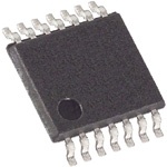
| 供应商器件封装 | 14-TSSOP |
| 共模抑制比—最小值 | 140 dB |
| 包装 | 管件 |
| 压摆率 | 1.2 V/µs |
| 可用增益调整 | 130 dB |
| 商标 | Analog Devices |
| 增益带宽生成 | 3.9 MHz |
| 增益带宽积 | 3.6MHz |
| 安装类型 | 表面贴装 |
| 安装风格 | SMD/SMT |
| 封装 | Tube |
| 封装/外壳 | 14-TSSOP(0.173",4.40mm 宽) |
| 封装/箱体 | TSSOP-14 |
| 工作温度 | -40°C ~ 125°C |
| 工作电源电压 | 5 V |
| 工厂包装数量 | 96 |
| 放大器类型 | 通用 |
| 最大工作温度 | + 125 C |
| 最小工作温度 | - 40 C |
| 标准包装 | 96 |
| 电压-电源,单/双 (±) | ±2.5 V ~ 15 V |
| 电压-输入失调 | 15µV |
| 电流-电源 | 400µA |
| 电流-输入偏置 | 400pA |
| 电流-输出/通道 | 10mA |
| 电源电压-最大 | 13 V |
| 电源电压-最小 | - 13.8 V |
| 电源电流 | 400 uA |
| 电路数 | 4 |
| 转换速度 | 1.2 V/us |
| 输入偏压电流—最大 | 1 nA |
| 输入电压范围—最大 | 36 V |
| 输入补偿电压 | 15 uV |
| 输出电流 | 10 mA |
| 输出类型 | - |
| 通道数量 | 4 Channel |


- 商务部:美国ITC正式对集成电路等产品启动337调查
- 曝三星4nm工艺存在良率问题 高通将骁龙8 Gen1或转产台积电
- 太阳诱电将投资9.5亿元在常州建新厂生产MLCC 预计2023年完工
- 英特尔发布欧洲新工厂建设计划 深化IDM 2.0 战略
- 台积电先进制程称霸业界 有大客户加持明年业绩稳了
- 达到5530亿美元!SIA预计今年全球半导体销售额将创下新高
- 英特尔拟将自动驾驶子公司Mobileye上市 估值或超500亿美元
- 三星加码芯片和SET,合并消费电子和移动部门,撤换高东真等 CEO
- 三星电子宣布重大人事变动 还合并消费电子和移动部门
- 海关总署:前11个月进口集成电路产品价值2.52万亿元 增长14.8%


PDF Datasheet 数据手册内容提取
4 MHz, 7 nV/√Hz, Low Offset and Drift, High Precision Amplifiers Data Sheet ADA4077-1/ADA4077-2/ADA4077-4 FEATURES PIN CONNECTION DIAGRAMS Offset voltage: NIC 1 8 NIC 25 μV maximum at 25°C (B grade, 8-lead SOIC, single/ dual) –IN 2 ADA4077-1 7 V+ 50 μV maximum at 25°C (A grade, 8-lead SOIC, single/ dual) +IN 3 TOP VIEW 6 OUT Of5fs0e μt Vvo mltaaxgiem durmift a: t 25°C (A grade, 14-lead SOIC, quad) NIC V= –NO4T IN(NToEtR tNoA SLcLaYle C)ON5NENCICTED. 10238-101 0.25 μV/°C maximum (B grade, 8-lead SOIC, single/dual) Figure 1. ADA4077-1, 8-Lead SOIC and 8-Lead MSOP 0.55 μV/°C maximum (A grade, 8-lead SOIC, single/dual) 0.75 μV/°C maximum (A grade, 14-lead SOIC, quad) OUT A 1 8 V+ ADA4077-2 MSL1 rated –IN A 2 7 OUT B TOP VIEW LLooww vinopltuatg bei anso cisuer rdeennts: i1t yn:A 6 .m9 anxVim/√uHmz t aytp TicA a=l 2at5 f° C= 1000 Hz +INV A– 34 (Not to Scale) 65 –+IINN BB 10238-001 CMRR, PSRR, and A > 120 dB minimum Figure 2. ADA4077-2, 8-Lead MSOP and 8-Lead SOIC V Low supply current: 400 μA per amplifier typical OUT A 1 14 OUT D Wide gain bandwidth product: 3.9 MHz at ±5 V –IN A 2 13 –IN D Dual-supply operation: +IN A 3 ADA4077-4 12 +IN D Specified at ±5 V to ±15 V TOP VIEW Operates at ±2.5 V to ±15 V V+ 4 (Not to Scale) 11 V– +IN B 5 10 +IN C Unity gain stable –IN B 6 9 –IN C NLoon pgh-taesrem r eovfefsresat lv oltage drift (10,000 hours): 0.5 μV typical OUT B 7 8 OUT C 10238-202 Temperature hysteresis: 1 μV typical Figure 3. ADA4077-4, 14-Lead TSSOP and 14-Lead SOIC APPLICATIONS The ADA4077-1 and ADA4077-2 are available in an 8-lead SOIC Process control front-end amplifiers package, including the B grade, and in an 8-lead MSOP (A grade Optical network control circuits only). The ADA4077-4 is offered in a 14-lead TSSOP and a 14-lead Instrumentation SOIC package. Precision sensors and controls 200 Precision filters VSY = ±5V 180 SOIC GENERAL DESCRIPTION 160 The single ADA4077-1, dual ADA4077-2, and quad ADA4077-4 ERS140 amplifiers feature extremely low offset voltage and drift, and low FI LI120 P input bias current, noise, and power consumption. Outputs are M A100 stable with capacitive loads of more than 1000 pF with no F O external compensation. ER 80 B Applications for this amplifier include sensor signal conditioning UM 60 N (such as thermocouples, resistance temperature detectors (RTDs), 40 strain gages), process control front-end amplifiers, and precision 20 diode power measurement in optical and wireless transmission 0 lsiynsete pmosw. Terheed A aDndA 4p0o7r7ta-1b/leA iDnAst4ru0m77e-n2t/aAtiDoAn,4 p0r7e7c-i4si oarne fuilsteefrus,l in –50–45–40–35–30–25–20–15–10–5VO0S (5µV10) 1520253035404550MORE 10238-103 and voltage or current measurement and level setting. Figure 4. Offset Voltage Distribution Unlike other amplifiers, the ADA4077-1/ADA4077-2/ Table 1. Evolution of Precision Devices by Generation ADA4077-4 have an MSL1 rating that is compliant with the most Op Amp First Second Third Fourth Fifth Sixth stringent of assembly processes, and they are specified over the Single OP07 OP77 OP177 OP1177 AD8677 ADA4077-1 extended industrial temperature range from −40°C to +125°C for Dual OP2177 ADA4077-2 Quad OP4177 ADA4077-4 the most demanding operating environments. R ev. E Document Feedback Information furnished by Analog Devices is believed to be accurate and reliable. However, no responsibility is assumed by Analog Devices for its use, nor for any infringements of patents or other One Technology Way, P.O. Box 9106, Norwood, MA 02062-9106, U.S.A. rights of third parties that may result from its use. Specifications subject to change without notice. No license is granted by implication or otherwise under any patent or patent rights of Analog Devices. Tel: 781.329.4700 ©2012–2017 Analog Devices, Inc. All rights reserved. Trademarks and registered trademarks are the property of their respective owners. Technical Support www.analog.com
ADA4077-1/ADA4077-2/ADA4077-4 Data Sheet TABLE OF CONTENTS Features .............................................................................................. 1 Typical Performance Characteristics ........................................... 11 Applications ....................................................................................... 1 Test Circuit ...................................................................................... 21 General Description ......................................................................... 1 Theory of Operation ...................................................................... 22 Pin Connection Diagrams ............................................................... 1 Applications Information .............................................................. 23 Revision History ............................................................................... 2 Output Phase Reversal ............................................................... 23 Specifications ..................................................................................... 3 Low Power Linearized RTD ...................................................... 23 Electrical Characteristics, ±5 V .................................................. 3 Proper Board Layout .................................................................. 23 Electrical Characteristics, ±15 V ................................................ 5 Long-Term Drift ......................................................................... 24 Absolute Maximum Ratings ....................................................... 7 Temperature Hysteresis ............................................................. 24 Thermal Resistance ...................................................................... 7 Outline Dimensions ....................................................................... 25 ESD Caution .................................................................................. 7 Ordering Guide .......................................................................... 27 Pin Configurations and Function Descriptions ........................... 8 REVISION HISTORY 5/2017—Rev. D to Rev. E 1/2014—Rev. A to Rev. B Changes to Features Section, Applications Section, and Figure 1 ... 1 Added ADA4077-1 ............................................................. Universal Added Maximum Reflow Temperature (MSL1 Rating) Changes to Features Section ............................................................ 1 Parameter and Note 2,Table 4; Renumbered Sequentially .......... 7 Added Figure 1; Renumbered Sequentially ................................... 1 Changes to Figure 5, Figure 6, and Table 6 ................................... 8 Changes to Table 2 ............................................................................. 3 Changes to Figure 24 and Figure 27 ............................................. 13 Changes to Table 3 ............................................................................. 4 Changes to Figure 29, Figure 30, Figure 31, Figure 32, Figure 33, Added Figure 5, Figure 6, and Table 6; Renumbered and Figure 34 ................................................................................... 14 Sequentially ........................................................................................ 7 Changes to Figure 66 ...................................................................... 20 Changes to Figure 17, Figure 20, and Figure 21 ......................... 11 Added Test Circuit Section and Figure 69; Renumbered Changes to Figure 65 ...................................................................... 19 Sequentially ..................................................................................... 22 Added Figure 67 and Figure 68 .................................................... 19 Added Long-Term Drift Section, Temperature Hysteresis Section, Changes to Output Phase Reversal Section and Figure 70 ....... 21 Figure 72, Figure 73, and Figure 74 ................................................. 24 Changes to Ordering Guide .......................................................... 24 Changes to Ordering Guide .......................................................... 27 10/2013—Rev. 0 to Rev. A 10/2016—Rev. C to Rev. D Added ADA4077-4 ............................................................. Universal Changes to Table 2 ............................................................................ 3 Changes to Features, General Description, and Figure 1 ............. 1 Changes to Table 3 ............................................................................ 5 Deleted Figure 2; Renumbered Sequentially ................................. 1 Changes to Figure 19 ...................................................................... 12 Added Figure 2 ................................................................................... 1 Changes to Figure 23 and Figure 26 ............................................. 13 Changes to Table 2 ............................................................................. 3 Changes to Figure 29, Figure 30, Figure 32, and Figure 33 ....... 14 Changes to Table 3 ............................................................................. 4 Changes to Table 4 ............................................................................. 6 6/2015—Rev. B to Rev. C Added Figure 6, Figure 7, and Table 7; Renumbered Change to Figure 63 ....................................................................... 18 Sequentially ........................................................................................ 8 Changes to Typical Performance Characteristics Section ........... 9 Changes to Figure 65 ...................................................................... 20 Updated Outline Dimensions ....................................................... 21 Changes to Ordering Guide .......................................................... 23 10/2012—Revision 0: Initial Version Rev. E | Page 2 of 27
Data Sheet ADA4077-1/ADA4077-2/ADA4077-4 SPECIFICATIONS ELECTRICAL CHARACTERISTICS, ±5 V V = ±5.0 V, V = 0 V, T = 25°C, unless otherwise noted. SY CM A Table 2. Parameter Symbol Test Conditions/Comments Min Typ Max Unit INPUT CHARACTERISTICS Offset Voltage V OS ADA4077-1/ADA4077-2 B Grade, SOIC 10 25 µV −40°C < T < +125°C 65 µV A A Grade, SOIC 15 50 µV −40°C < T < +125°C 105 µV A A Grade, MSOP 50 90 µV −40°C < T < +125°C 220 µV A ADA4077-4 A Grade, SOIC 15 50 µV −40°C < T < +125°C 105 µV A A Grade, TSSOP 15 120 µV −40°C < T < +125°C 220 µV A Offset Voltage Drift ∆V /∆T −40°C < T < +125°C OS A ADA4077-1/ADA4077-2 B Grade, SOIC 0.1 0.25 µV/°C A Grade, SOIC 0.25 0.55 µV/°C A Grade, MSOP 0.5 1.2 µV/°C ADA4077-4 A Grade, SOIC 0.4 0.75 µV/°C A Grade, TSSOP 0.5 1.2 µV/°C Input Bias Current I −1 −0.4 +1 nA B −40°C < T < +125°C −1.5 +1.5 nA A Input Offset Current I −0.5 +0.1 +0.5 nA OS −40°C < T < +125°C −1 +1 nA A Input Voltage Range −3.8 +3 V Common-Mode Rejection Ratio CMRR V = −3.8 V to +3 V 122 140 dB CM V = −3.8 V to +3 V, −40°C < T < +85°C 120 dB CM A V = −3.8 V to +2.8 V, 85°C < T < 125°C 120 dB CM A Large Signal Voltage Gain Av R = 2 kΩ, V = −3.0 V to +3.0 V 121 130 dB L O −40°C < T < +125°C 120 dB A Input Capacitance C Common mode 5 pF INCM Input Resistance R Common mode 70 GΩ IN OUTPUT CHARACTERISTICS Output Voltage High V I = 1 mA 3.8 V OH L −40°C < T < +125°C 3.7 V A Output Voltage Low V I = 1 mA −3.8 V OL L −40°C < T < +125°C −3.7 V A Output Current I V < 1.6 V ±10 mA OUT DROPOUT Short-Circuit Current I T = 25°C 22 mA SC A Closed-Loop Output Impedance Z f = 1 kHz, A = +1 0.05 Ω OUT V POWER SUPPLY Power Supply Rejection Ratio PSRR V = ±2.5 V to ±18 V 123 128 dB S −40°C < T < +125°C 120 dB A Supply Current per Amplifier I V = 0 V 400 450 µA SY O −40°C < T < +125°C 650 µA A Rev. E | Page 3 of 27
ADA4077-1/ADA4077-2/ADA4077-4 Data Sheet Parameter Symbol Test Conditions/Comments Min Typ Max Unit DYNAMIC PERFORMANCE Slew Rate SR R = 2 kΩ 1.2 V/µs L Settling Time to 0.1% t V = 1 V step, R = 2 kΩ, A = −1 3 µs S IN L V Gain Bandwidth Product GBP V = 10 mV p-p, R = 2 kΩ, A = +100 3.9 MHz IN L V Unity-Gain Crossover UGC V = 10 mV p-p, R = 2 kΩ, A = +1 3.9 MHz IN L V −3 dB Closed-Loop Bandwidth −3 dB A = +1, V = 10 mV p-p, R = 2 kΩ 5.9 MHz V IN L Phase Margin ΦM V = 10 mV p-p, R = 2 kΩ, A = +1 55 Degrees IN L V Total Harmonic Distortion Plus Noise THD + N V = 1 V rms, A = +1, R = 2 kΩ, f = 1 kHz 0.004 % IN V L NOISE PERFORMANCE Voltage Noise e p-p 0.1 Hz to 10 Hz 0.25 µV p-p n Voltage Noise Density e f = 1 Hz 13 nV/√Hz n f = 100 Hz 7 nV/√Hz f = 1000 Hz 6.9 nV/√Hz Current Noise Density i f = 1 kHz 0.2 pA/√Hz n MULTIPLE AMPLIFIERS CHANNEL SEPARATION C f = 1 kHz, R = 10 kΩ −125 dB S L Rev. E | Page 4 of 27
Data Sheet ADA4077-1/ADA4077-2/ADA4077-4 ELECTRICAL CHARACTERISTICS, ±15 V V = ±15 V, V = 0 V, T = 25°C, unless otherwise noted. SY CM A Table 3. Parameter Symbol Test Conditions/Comments Min Typ Max Unit INPUT CHARACTERISTICS Offset Voltage V OS ADA4077-1/ADA4077-2 B Grade, SOIC 10 35 µV −40°C < T < +125°C 65 µV A A Grade, SOIC 15 50 µV −40°C < T < +125°C 105 µV A A Grade, MSOP 50 90 µV −40°C < T < +125°C 220 µV A ADA4077-4 A Grade, SOIC 15 50 µV −40°C < T < +125°C 105 µV A A Grade, TSSOP 15 120 µV −40°C < T < +125°C 220 µV A Offset Voltage Drift ∆V /∆T OS ADA4077-1/ADA4077-2 B Grade, SOIC −40°C < T < +125°C 0.1 0.25 µV/°C A A Grade, SOIC −40°C < T < +125°C 0.25 0.55 µV/°C A A Grade, MSOP −40°C < T < +125°C 0.5 1.2 µV/°C A ADA4077-4 A Grade, SOIC −40°C < T < +125°C 0.4 0.75 µV/°C A A Grade, TSSOP −40°C < T < +125°C 0.5 1.2 µV/°C A Input Bias Current I −1 −0.4 +1 nA B −40°C < T < +125°C −1.5 +1.5 nA A Input Offset Current I −0.5 +0.1 +0.5 nA OS −40°C < T < +125°C −1 +1 nA A Input Voltage Range −13.8 +13 V Common-Mode Rejection Ratio CMRR V = −13.8 V to +13 V 132 150 dB CM −40°C < T < +125°C 130 dB A Large Signal Voltage Gain Av ADA4077-1/ADA4077-2 (SOIC, MSOP) R = 2 kΩ, V = −13.0 V to +13.0 V 125 130 dB L O −40°C < T < +125°C 120 dB A ADA4077-4 (SOIC, TSSOP) R = 2 kΩ, V = −13.0 V to +13.0 V 122 130 dB L O −40°C < T < +125°C 120 dB A Input Capacitance C Differential mode 3 pF INDM C Common mode 5 pF INCM Input Resistance R Common mode 70 GΩ IN OUTPUT CHARACTERISTICS Output Voltage High V I = 1 mA 13.8 V OH L −40°C < T < +125°C 13.7 V A Output Voltage Low V I = 1 mA −13.8 V OL L −40°C < T < +125°C −13.7 V A Output Current I V < 1.2 V ±10 mA OUT DROPOUT Short-Circuit Current I T = 25°C 22 mA SC A Closed-Loop Output Impedance Z f = 1 kHz, A = +1 0.05 Ω OUT V Rev. E | Page 5 of 27
ADA4077-1/ADA4077-2/ADA4077-4 Data Sheet Parameter Symbol Test Conditions/Comments Min Typ Max Unit POWER SUPPLY Power Supply Rejection Ratio PSRR V = ±2.5 V to ±18 V 123 128 dB S −40°C < T < +125°C 120 dB A Supply Current per Amplifier I V = 0 V 400 500 µA SY O −40°C < T < +125°C 650 µA A DYNAMIC PERFORMANCE Slew Rate SR R = 2 kΩ 1.2 V/µs L Settling Time to 0.01% t V = 10 V p-p, R = 2 kΩ, A = −1 16 µs s IN L V Settling Time to 0.1% t V = 10 V p-p, R = 2 kΩ, A = −1 10 µs s IN L V Gain Bandwidth Product GBP V = 10 mV p-p, R = 2 kΩ, A = +100 3.6 MHz IN L V Unity-Gain Crossover UGC V = 10 mV p-p, R = 2 kΩ, A = +1 3.9 MHz IN L V −3 dB Closed-Loop Bandwidth −3 dB A = +1, V = 10 mV p-p, R = 2 kΩ 5.5 MHz V IN L Phase Margin ΦM V = 10 mV p-p, R = 2 kΩ, A = +1 58 Degrees IN L V Total Harmonic Distortion Plus Noise THD + N V = 1 V rms, A = +1, R = 2 kΩ, 0.004 % IN V L f = 1 kHz NOISE PERFORMANCE Voltage Noise e p-p 0.1 Hz to 10 Hz 0.25 µV p-p n Voltage Noise Density e f = 1 Hz 13 nV/√Hz n f = 100 Hz 7 nV/√Hz f = 1000 Hz 6.9 nV/√Hz Current Noise Density i f = 1 kHz 0.2 pA/√Hz n MULTIPLE AMPLIFIERS CHANNEL SEPARATION C f = 1 kHz, R = 10 kΩ −125 dB S L Rev. E | Page 6 of 27
Data Sheet ADA4077-1/ADA4077-2/ADA4077-4 ABSOLUTE MAXIMUM RATINGS THERMAL RESISTANCE Table 4. Parameter Rating θ is specified for the worst case conditions, that is, a device JA Supply Voltage 36 V soldered in a circuit board for surface-mount packages. Input Voltage ±V SY Table 5. Thermal Resistance Input Current1 ±10 mA Package Type θ θ Unit Differential Input Voltage ±V JA JC SY 8-Lead MSOP 190 44 °C/W Output Short-Circuit Duration to GND Indefinite 8-Lead SOIC 158 43 °C/W Storage Temperature Range −65°C to +150°C 14-Lead TSSOP 240 43 °C/W Operating Temperature Range −40°C to +125°C 14-Lead SOIC 115 36 °C/W Junction Temperature Range −65°C to +150°C Maximum Reflow Temperature (MSL1 Rating)2 260°C Lead Temperature, Soldering (10 sec) 300°C ESD CAUTION Electrostatic Discharge (ESD) Human Body Model (HBM)3 6 kV Field Induced Charge Device Model (FICDM)4 1.25 kV 1 The input pins have clamp diodes to the power supply pins and to each other. Limit the input current to 10 mA or less whenever input signals exceed the power supply rail by 0.3 V. 2 IPC/JEDEC J-STD-020 applicable standard. 3 ESDA/JEDEC JS-001-2011 applicable standard. 4 JESD22-C101 (ESD FICDM standard of JEDEC) applicable standard. Stresses at or above those listed under Absolute Maximum Ratings may cause permanent damage to the product. This is a stress rating only; functional operation of the product at these or any other conditions above those indicated in the operational section of this specification is not implied. Operation beyond the maximum operating conditions for extended periods may affect product reliability. Rev. E | Page 7 of 27
ADA4077-1/ADA4077-2/ADA4077-4 Data Sheet PIN CONFIGURATIONS AND FUNCTION DESCRIPTIONS NIC 1 8 NIC NIC 1 8 NIC –IN 2 ADA4077-1 7 V+ –IN 2 ADA4077-1 7 V+ +IN 3 TOP VIEW 6 OUT +IN 3 TOP VIEW 6 OUT NIC V=– NO4T IN(NTEoRt tNoA SLcLaYl eC)ON5NENCITCED. 10238-205 NIC =V –NO4T IN(NTEoRt tNoA SLcLaYl eC)ON5NENCICTED. 10238-105 Figure 5. ADA4077-1 Pin Configuration, 8-Lead MSOP (RM-8) Figure 6. ADA4077-1 Pin Configuration, 8-Lead SOIC (R-8) Table 6. ADA4077-1 Pin Function Descriptions, 8-Lead MSOP and 8-Lead SOIC Pin No. Mnemonic Description 1, 5, 8 NIC Not internally connected. 2 −IN Inverting Input. 3 +IN Noninverting Input. 4 V− Negative Supply Voltage. 6 OUT Output. 7 V+ Positive Supply Voltage. Rev. E | Page 8 of 27
Data Sheet ADA4077-1/ADA4077-2/ADA4077-4 OUT A 1 8 V+ OUT A 1 8 V+ –IN A 2 ADA4077-2 7 OUT B –IN A 2 ADA4077-2 7 OUT B TOP VIEW +INV A– 34 (Not to Scale) 65 +–IINN BB 10238-004 +INV A– 34 (NToOt Pto V SIEcWale) 65 –+IINN BB 10238-005 Figure 7. ADA4077-2 Pin Configuration, 8-Lead MSOP Figure 8. ADA4077-2 Pin Configuration, 8-Lead SOIC Table 7. ADA4077-2 Pin Function Descriptions, 8-Lead MSOP and 8-Lead SOIC Pin No. Mnemonic Description 1 OUT A Output Channel A. 2 −IN A Inverting Input Channel A. 3 +IN A Noninverting Input Channel A. 4 V− Negative Supply Voltage. 5 +IN B Noninverting Input Channel B. 6 −IN B Inverting Input Channel B. 7 OUT B Output Channel B. 8 V+ Positive Supply Voltage. Rev. E | Page 9 of 27
ADA4077-1/ADA4077-2/ADA4077-4 Data Sheet OUT A 1 14 OUT D OUT A 1 14 OUT D –IN A 2 13 –IN D –IN A 2 13 –IN D +IN A 3 ADA4077-4 12 +IN D +IN A 3 ADA4077-4 12 +IN D TOP VIEW V+ 4 TOP VIEW 11 V– V+ 4 (Not to Scale) 11 V– +IN B 5 (Not to Scale) 10 +IN C O+–UIINNT BBB 567 1890 O–+IIUNNT CC C 10238-206 O–UINT BB 67 98 –OIUNT C C 10238-207 Figure 9. ADA4077-4 Pin Configuration, 14-Lead TSSOP Figure 10. ADA4077-4 Pin Configuration, 14-Lead SOIC Table 8. ADA4077-4 Pin Function Descriptions, 14-Lead TSSOP and 14-Lead SOIC Pin No. Mnemonic Description 1 OUT A Output Channel A. 2 −IN A Negative Input Channel A. 3 +IN A Positive Input Channel A. 4 V+ Positive Supply Voltage. 5 +IN B Positive Input Channel B. 6 −IN B Negative Input Channel B. 7 OUT B Output Channel B. 8 OUT C Output Channel C. 9 −IN C Negative Input Channel C. 10 +IN C Positive Input Channel C. 11 V− Negative Supply Voltage. 12 +IN D Positive Input Channel D. 13 −IN D Negative Input Channel D. 14 OUT D Output Channel D. Rev. E | Page 10 of 27
Data Sheet ADA4077-1/ADA4077-2/ADA4077-4 TYPICAL PERFORMANCE CHARACTERISTICS 120 140 MVSSYO =P ±5V VSY = ±15V 120 MSOP 100 S S R R100 E E FI 80 FI LI LI MP MP 80 A A F 60 F O O R R 60 E E MB 40 MB U U 40 N N 20 20 0 0 –50–45–40–35–30–25–20–15–10–5VO0S (5µV)101520253035404550MORE 10238-006 –50–45–40–35–30–25–20–15–10–5V0OS5 (µ10V)1520253035404550MORE 10238-003 Figure 11. ADA4077-2 Offset Voltage (VOS) Distribution, VSY = ±5 V Figure 14. ADA4077-2 Offset Voltage (VOS) Distribution, VSY = ±15 V 200 200 180 SVOSYIC = ±5V 180 SVOSYIC = ±15V 160 160 S S ER140 ER140 FI FI PLI120 PLI120 M M FA100 FA100 O O ER 80 ER 80 B B M M U 60 U 60 N N 40 40 20 20 0 0 –50–45–40–35–30–25–20–15–10–5VO0S (5µV)101520253035404550MORE 10238-144 –50–45–40–35–30–25–20–15–10–5VO0S (5µV)101520253035404550MORE 10238-009 Figure 12. Offset Voltage (VOS) Distribution, VSY = ±5 V Figure 15. Offset Voltage (VOS) Distribution, VSY = ±15 V 20 15 VSY = ±5V VSY = ±15V 15 10 10 5 V) V) (µOS 5 (µOS 0 V V 0 –5 –5 –10 –10–50 –25 0 TEMP25ERATUR5E0 (°C) 75 100 125 10238-210 –15–50 –25 0 TEMP25ERATUR5E0 (°C) 75 100 125 10238-213 Figure 13. Offset Voltage (VOS) vs. Temperature, VSY = ±5 V Figure 16. Offset Voltage (VOS) vs. Temperature, VSY = ±15 V Rev. E | Page 11 of 27
ADA4077-1/ADA4077-2/ADA4077-4 Data Sheet 50 70 45 VSY = ±15V, ±5V SVOSYIC =, ±A1 G5VR,A ±D5VE TSSOPAND MSOP, A GRADE 60 40 S S ER35 ER50 FI FI MPLI30 MPLI40 A A F25 F O O ER 20 ER 30 B B M M U15 U20 N N 10 10 5 0 0 00.050.100.150.200.250.300.35T0.40CV0.45OS0.50 (µ0.55V/°0.60C)0.650.700.750.800.850.900.951.00 10238-130 00.050.100.150.200.250.300.35T0.40CV0.45OS0.50 (µ0.55V/°0.60C)0.650.700.750.800.850.900.951.00 10238-008 Figure 17. TCVOS Distribution ([TSSOP and MSOP, A Grade) Figure 20. TCVOS Distribution (SOIC, A Grade) 10 140 VSY = ±15V, ±5V SOIC, B GRADE 120 5 S R100 E FI LI V (µV)OS 0 R OFAMP 6800 E B M –5 NU 40 20 –100 5 10 15VSY (V)20 25 30 35 10238-134 0 00.050.100.150.200.250.300.35T0.40CV0.45OS0.50 (µ0.55V/°0.60C)0.650.700.750.800.850.900.951.00 10238-308 Figure 18. Offset Voltage (VOS) vs. Power Supply Voltage (VSY) Figure 21. TCVOS Distribution (SOIC, B Grade) 100 0.6 VS = ±15V 80 –15V ≤ VCM ≤ +15V 60 40 0.4 20 V) A) V (µOS 0 I (mSY –20 0.2 –40 –40°C VO = 0V –60 +25°C +85°C AVERAGE +125°C –80 AVERAGE +3σ AVERAGE –3σ –100–15–13–11 –9 –7 –5 –3 V–C1M (1V) 3 5 7 9 11 13 15 10238-419 00 2 4 6 8 10121416V1S8Y 2(0V)222426283032343638 10238-218 Figure 19. Offset Voltage (VOS) vs. Common-Mode Voltage (VCM), VSY = ±15 V Figure 22. Supply Current per Amplifier (ISY) vs. Power Supply Voltage (VSY) Rev. E | Page 12 of 27
Data Sheet ADA4077-1/ADA4077-2/ADA4077-4 4.15 14.15 VOH = 1mA VOH = 1mA VOL = 1mA VOL = 1mA 4.10 14.10 V) V) G (4.05 G ( 14.05 N N WI WI S4.00 S 14.00 E E G G TA3.95 TA 13.95 L L O O V V T 3.90 T 13.90 U U P P T T U3.85 U 13.85 O O 3.80 13.80 VS = ±5V VS = ±15V 3.75–50 –25 0 TEM2P5ERATUR5E0 (°C) 75 100 125 10238-423 13.75–50 –25 0 TEM2P5ERATUR5E0 (°C) 75 100 125 10238-426 Figure 23. Output Voltage Swing vs. Temperature, VSY = ±5 V Figure 26. Output Voltage Swing vs. Temperature, VSY = ±15 V 350 400 VSY = ±5V VSY = ±15V 300 350 S S 300 R 250 R E E FI FI LI LI 250 MP 200 MP F A F A 200 R O 150 R O E E 150 B B M M U 100 U N N 100 50 50 0 0 –1.0 –0.9 –0.8 IN–0.7PUT B–0.6IAS C–0.5URRE–0.4NT (n–0.3A) –0.2 –0.1 0 10238-013 –1 –0.9 –0.8 IN–0.7PUT B–0.6IAS C–0.5URRE–0.4NT (n–0.3A) –0.2 –0.1 0 10238-016 Figure 24. Input Bias Current Distribution, VSY = ±5 V Figure 27. Input Bias Current Distribution, VSY = ±15 V 0 0 VSY = ±5V VSY = ±15V –0.1 –0.1 –0.2 –0.2 –IB +IB –IB A) –0.3 A) –0.3 n n (B (B I –0.4 I –0.4 +IB –0.5 –0.5 –0.6 –0.6 –0.7–50 –25 0 TEMP25ERATUR5E0 (°C) 75 100 125 10238-014 –0.7–50 –25 0 TEMP25ERATUR5E0 (°C) 75 100 125 10238-017 Figure 25. Input Bias Current (IB) vs. Temperature, VSY = ±5 V Figure 28. Input Bias Current (IB) vs. Temperature, VSY = ±15 V Rev. E | Page 13 of 27
ADA4077-1/ADA4077-2/ADA4077-4 Data Sheet 10k 100k ISINK = –40°C ISINK = –40°C ISINK = +25°C ISINK = +25°C ISINK = +85°C ISINK = +85°C V) ISINK = +125°C V) ISINK = +125°C m m E ( E ( G G LTA LTA10k O O V V T T U 1k U O O P P O O R R T D T D 1k U U P P T T U U O O VSY = ±5V VSY = ±15V –40°C ≤ T ≤ +125°C –40°C ≤ T ≤ +125°C 100 100 0.001 0.01 0.1ILOAD (mA)1 10 100 10238-429 0.001 0.01 0.1ILOAD (mA)1 10 100 10238-432 Figure 29. Output Dropout Voltage vs. ILOAD, Sink Current, VSY = ±5 V Figure 32. Output Dropout Voltage vs. ILOAD, Sink Current, VSY = ±15 V mV)10k IIIISSSSOOOOUUUURRRRCCCCEEEE ==== +++–428155025°°°CCC°C mV)100k IIIISSSSOOOOUUUURRRRCCCCEEEE ==== +++–428105525°°°CCC°C OUTPUT DROPOUT VOLTAGE (1k OUTPUT DROPOUT VOLTAGE (101kk –40°C ≤ TV ≤S Y+ 1=2 ±55°CV VSY = ±15V 1000.001 0.01 0.1ILOAD (mA)1 10 100 10238-430 1000.001 0.01 0.1ILOAD (mA)1 –40°C 1≤0 T ≤ +125°C100 10238-433 Figure 30. Output Dropout Voltage vs. ILOAD, Source Current, VSY = ±5 V Figure 33. Output Dropout Voltage vs. ILOAD, Source Current, VSY = ±15 V 150 150 150 150 GAIN=0pF GAIN=100pF GAIN=200pF GAIN=0pF GAIN=100pF GAIN=200pF PHASE=0pF PHASE=100pF PHASE=200pF PHASE=0pF PHASE=100pF PHASE=200pF 100 100 100 100 GAIN (dB) 50 50 N (Degrees) GAIN (dB) 50 50 N (Degrees) OOP 0 0 ARGI OOP 0 0 ARGI OPEN-L –50 AVRSVLY == = 2– k±1Ω5V –50 PHASE M OPEN-L –50 AVRSVLY == = 2– k±1Ω15V –50 PHASE M –100 –100 –100 –100 –15010k 100k FREQU1EMNCY (Hz) 10M 100M–150 10238-227 –15010k 100k FREQU1EMNCY (Hz) 10M 100M–150 10238-230 Figure 31. Open-Loop Gain and Phase Margin vs. Frequency, VSY = ±5 V Figure 34. Open-Loop Gain and Phase Margin vs. Frequency, VSY = ±15 V Rev. E | Page 14 of 27
Data Sheet ADA4077-1/ADA4077-2/ADA4077-4 133 140 132 VSY = ±5VTO ±15V VVSSYY == ±±155VV 120 131 100 130 PSRR (dB)112289 CMRR (dB) 6800 127 40 126 20 125 124–50 –25 0 TEMP2E5RATUR5E0 (°C) 75 100 125 10238-035 0100 1k F1R0EkQUENCY1 (0H0zk) 1M 10M 10238-029 Figure 35. PSRR vs. Temperature, VSY = ±5 V to ±15 V Figure 38. CMRR vs. Frequency, VSY = ±5 V and VSY = ±15 V 120 120 VSY = ±5V VSY = ±15V 100 100 80 80 dB) 60 dB) 60 PSRR– R ( R ( R R PS 40 PSRR– PS 40 PSRR+ PSRR+ 20 20 0 0 –20100 1k F1R0EkQUENCY1 (0H0zk) 1M 10M 10238-034 –20100 1k F1R0EkQUENCY1 (0H0zk) 1M 10M 10238-037 Figure 36. PSRR vs. Frequency, VSY = ±5 V Figure 39. PSRR vs. Frequency, VSY = ±15 V 152 159 151 VSY = ±5V VSY = ±15V 150 158 149 157 148 B) B) R (d147 R (d156 MR146 MR C C 145 155 144 143 154 142 141–50 –25 0 TEMP25ERATUR5E0 (°C) 75 100 125 10238-030 153–50 –25 0 TEMP25ERATUR5E0 (°C) 75 100 125 10238-033 Figure 37. CMRR vs. Temperature, VSY = ±5 V Figure 40. CMRR vs. Temperature, VSY = ±15 V Rev. E | Page 15 of 27
ADA4077-1/ADA4077-2/ADA4077-4 Data Sheet 50 50 G = 100 VSY = ±5V G = 100 VSY = ±15V 40 40 30 30 B) G = 10 B) G = 10 d 20 d 20 N ( N ( AI 10 AI 10 G G P G = 1 P G = 1 O 0 O 0 O O L L D- –10 D- –10 E E S S O –20 O –20 L L C C –30 –30 –40 –40 –501k 10k F1R00EkQUENCY (1HMz) 10M 100M 10238-028 –501k 10k F1R00EkQUENCY (1HMz) 10M 100M 10238-031 Figure 41. Closed-Loop Gain vs. Frequency, VSY = ±5 V Figure 44. Closed-Loop Gain vs. Frequency, VSY = ±15 V 1k 1k VSY = ±5V VSY = ±15V 100 100 AV = +100 AV = +100 10 AV = +10 10 AV = +10 Ω) Ω) (UT 1 AV = +1 (UT 1 AV = +1 O O Z Z 0.1 0.1 0.01 0.01 0.001 0.001 100 1k F1R0EkQUENCY1 (0H0zk) 1M 10M 10238-036 100 1k F1R0EkQUENCY1 (0H0zk) 1M 10M 10238-039 Figure 42. Output Impedance (ZOUT) vs. Frequency, VSY = ±5 V Figure 45. Output Impedance (ZOUT) vs. Frequency, VSY = ±15 V VOLTAGE (0.2V/DIV)0V VVACRSIVLLNY === == 23+ 1k0±1VΩ05 pVpF-p VOLTAGE (1V/DIV)0V CAVVRSIVLLNY === == 23+ 4±k01VΩ01 p5pVF-p TIME (100µs/DIV) 10238-040 TIME (100µs/DIV) 10238-043 Figure 43. Large Signal Transient Response, VSY = ±5 V Figure 46. Large Signal Transient Response, VSY = ±15 V Rev. E | Page 16 of 27
Data Sheet ADA4077-1/ADA4077-2/ADA4077-4 0.20 0.20 0.15 0.15 0.10 0.10 V) 0.05 V) 0.05 E ( E ( G G A 0 A 0 T T L L O O V–0.05 V–0.05 VSY = ±5V VSY = ±15V –0.10 VIN = 100mV p-p –0.10 VIN = 100mV p-p AV = +1 AV = +1 LOAD = 2kΩ||1000pF LOAD = 2kΩ||1000pF –0.15 –0.15 –0.20 –0.20 –0.2 –0.1 0 0.1 0.2TIM0E. 3(ms)0.4 0.5 0.6 0.7 0.8 10238-344 –0.2 –0.1 0 0.1 0.2TIM0E. 3(ms)0.4 0.5 0.6 0.7 0.8 10238-247 Figure 47. Small Signal Transient Response, VSY = ±5 V Figure 50. Small Signal Transient Response, VSY = ±15 V V) 0.5 0.5 35 E ( G TA INPUT 0 30 L 0 O V T –0.5 25 U INP–0.5 AVVRSIVLNY == == 1– 20±10k500ΩV0mV 5 GE (V) INPUT (V)–––211...050 VLVAOSIVNY A = ==D – 2 ±1=010 0150m0VkVΩ p-p 112050 OUTPUT (V) 3 A T L O –2.5 5 V OUTPUT 1 UT P –3.0 0 T U TIME (10µs/DIV) –1 O 10238-046 –3.5–10 0 10 20 30TIME40 (µs)50 60 70 80 90–5 10238-248 Figure 48. Positive Overload Recovery, VSY = ±5 V Figure 51. Positive Overload Recovery, VSY = ±15 V V) 0.5 V) 0.5 E ( E ( G G A INPUT A INPUT OLT 0 OLT 0 V V UT UT NP–0.5 NP–0.5 I I OUTPUT 1 0 OUTPUT V) V) E ( E ( G G –1 A –5 A AVVRSIVLNY == == 1– 20±10k500ΩV0mV –3 UTPUT VOLT AVVRSIVLNY == == 1– 20±10k100Ω50mVV –10 UTPUT VOLT TIME (10µs/DIV) –5 O 10238-047 TIME (10µs/DIV) –15 O 10238-051 Figure 49. Negative Overload Recovery, VSY = ±5 V Figure 52. Negative Overload Recovery, VSY = ±15 V Rev. E | Page 17 of 27
ADA4077-1/ADA4077-2/ADA4077-4 Data Sheet 40 40 VSY = ±5V VSY = ±15V 35 RL = 2kΩ 35 RL = 2kΩ 30 30 %) %) T ( 25 T ( 25 O O O O H 20 H 20 S S R R E E V 15 V 15 O O OS+ OS+ OS– OS– 10 10 5 5 01p 10p LOAD CAP1A00CpITANCE (F) 1n 10n 10238-250 01p 10p LOAD CAP1A00CpITANCE (F) 1n 10n 10238-253 Figure 53. Small Signal Overshoot vs. Load Capacitance, VSY = ±5 V Figure 56. Small Signal Overshoot vs. Load Capacitance, VSY = ±15 V 0.05 0.25 0.04 0.20 0.03 0.15 VSY = ±5V UT (V) VRILN == 21kVΩ p-p 00..0012 PUT (V) UT (V) 00..0150 PUT (V) P T P T N U N U I O I O 0 0 –0.01 VSY = ±15V –0.05 VIN = 10V p-p –0.02 RL = 2kΩ –0.10 TIME (1µs/DIV) –0.03 10238-251 TIME (1µs/DIV) –0.15 10238-254 Figure 54. Positive 0.1% Settling Time, VSY = ±5 V Figure 57. Positive 0.1% Settling Time, VSY = ±15 V 0.05 0.25 0.04 0.20 VSY = ±5V VSY = ±15V VIN = 1V p-p 0.03 VIN = 10V p-p 0.15 RL = 2kΩ RL = 2kΩ INPUT (V) 00..0012 OUTPUT (V) INPUT (V) 00..0150 OUTPUT (V) 0 0 –0.01 –0.05 –0.02 –0.10 TIME (1µs/DIV) –0.03 10238-252 TIME (1µs/DIV) –0.15 10238-255 Figure 55. Negative 0.1% Settling Time, VSY = ±5 V Figure 58. Negative 0.1% Settling Time, VSY = ±15 V Rev. E | Page 18 of 27
Data Sheet ADA4077-1/ADA4077-2/ADA4077-4 1k 100 VSY = ±15V VSY = ±5V 90 VSY = ±5V Hz) AV = +1 Hz) 80 VSY = ±15V √ √ V/ V/ Y (n 100 R (n 70 T E SI N 60 N R E O D C 50 E E S S OI OI 40 N N GE 10 GE 30 A A T T L L 20 O O V V 10 110 100 1kFREQU1E0NkCY (Hz1)00k 1M 10M 10238-053 00 0.5 1.0FREQUE1.N5CY (Hz)2.0 2.5 3.0 10238-153 Figure 59. Voltage Noise Density vs. Frequency, VSY = ±5 V and VSY = ±15 V Figure 62. Voltage Noise Corner vs. Frequency, VSY = ±15 V and VSY = ±5 V 1 100 VSY = ±5V VSY = ±15V 10 0.1 E (%) BANDWIDTH=80kHz E (%) 1 BBAANNDDWWIIDDTTHH==8500k0kHHzz NOIS 0.01 BANDWIDTH=500kHz NOIS 0.1 + + D D H H T T 0.01 0.001 0.001 0.000110 100 FREQUE1kNCY (Hz) 10k 100k 10238-155 0.000110 100 FREQUE1kNCY (Hz) 10k 100k 10238-158 Figure 60. THD + Noise vs. Frequency, VSY = ±5 V Figure 63. THD + Noise vs. Frequency, VSY = ±15 V VSY = ±5V VSY = ±15V V) V) DI DI V/ V/ GE (50n GE (50n OLTA OLTA UT V UT V NP NP I I TIME (1s/DIV) 10238-054 TIME (1s/DIV) 10238-058 Figure 61. 0.1 Hz to 10 Hz Noise, VSY = ±5 V Figure 64. 0.1 Hz to 10 Hz Noise, VSY = ±15 V Rev. E | Page 19 of 27
ADA4077-1/ADA4077-2/ADA4077-4 Data Sheet 200 100 100 VSY = ±15V VSY = ±15V –15V ≤ VCM ≤ +15V 0 TA = 25°C Hz) √ –100 A/ p –200 Y ( 10 T A) –300 ENSI I (pB ––540000 OISE D N –600 T 1 N E –700 R R –800 MEAN +3σ CU MEAN –900 MEAN –3σ –1000–20 –15 –10 –5 VCM0 (V) 5 10 15 20 10238-219 0.11 10 F1R0E0QUENCY (1Hkz) 10k 100k 10238-267 Figure 65. Input Bias Current (IB) vs. Common-Mode Voltage (VCM) Figure 67. Current Noise Density, VSY = ±15 V 0 100 VSY = ±5V –20 Hz) EPARATION (dB) –––864000 E DENSITY (pA/√ 10 S S EL –100 NOI CHANN ––114200 VVASIVNY = == + 1±101V5 Vp-p CURRENT 1 RL = 10kΩ –160100 1k FREQU1E0NkCY (Hz) 100k 1M 10238-244 0.11 10 F1R0E0QUENCY (1Hkz) 10k 100k 10238-268 Figure 66. Channel Separation, VSY = ±15 V (See Figure 69) Figure 68. Current Noise Density, VSY = ±5 V Rev. E | Page 20 of 27
Data Sheet ADA4077-1/ADA4077-2/ADA4077-4 TEST CIRCUIT 10kΩ VCC VCC 1kΩ – – + + VIN CHV AEE 2kΩ 2kΩ VECCCEHHH BCD,, 10238-469 Figure 69 Test Circuit for Channel Separation vs. Frequency Rev. E | Page 21 of 27
ADA4077-1/ADA4077-2/ADA4077-4 Data Sheet THEORY OF OPERATION The ADA4077-1/ADA4077-2/ADA4077-4 are the sixth generation The ADA4077-1/ADA4077-2/ADA4077-4 have an operating of the Analog Devices, Inc., industry-standard OP07 amplifier temperature range of −40°C to +125°C with an MSL1 rating, which family. The ADA4077-1/ADA4077-2/ADA4077-4 are high pre- is as wide as any similar device in a plastic surface-mount package. cision, low noise operational amplifiers with a combination of This MSL1 rating is increasingly important as printed circuit extremely low offset voltage and very low input bias currents. board (PCB) and overall system sizes continue to shrink, causing Unlike JFET amplifiers, the low bias and offset currents are internal system temperatures to rise. relatively insensitive to ambient temperatures, even up to 125°C. In the ADA4077-1/ADA4077-2/ADA4077-4, the power con- The Analog Devices proprietary process technology and linear sumption is reduced by a factor of four compared to the OP177, design expertise have produced high voltage amplifiers with and the bandwidth and slew rate are both increased by a factor superior performance to the OP07/OP77/OP177/OP1177 in of six. The low power dissipation and very stable performance tiny, 8-lead SOIC and 8-lead MSOP packages (ADA4077-1 and vs. temperature also reduce warmup drift errors to insignificant ADA4077-2) and 14-lead TSSOP and 14-lead SOIC packages levels. (ADA4077-4). Despite their small size, the ADA4077-1/ Inputs are protected internally from overvoltage conditions ADA4077-2/ADA4077-4 offer numerous improvements, referenced to either supply rail. Like any high performance including low wideband noise, wide bandwidth, lower offset and amplifier, maximum performance is achieved by following offset drift, lower input bias current, and complete freedom from appropriate circuit and PCB guidelines. phase inversion. Rev. E | Page 22 of 27
Data Sheet ADA4077-1/ADA4077-2/ADA4077-4 APPLICATIONS INFORMATION OUTPUT PHASE REVERSAL +15V 500Ω FULL-SCALE ADJ Phase reversal is defined as a change of polarity in the amplifier 0.1µF transfer function. Many operational amplifiers exhibit phase ADR4525 0.1µF reversal when the voltage applied to the input is greater than the 4.12kΩ 4.37kΩ 200Ω maximum common-mode voltage. In some instances, this phase 6 reversal can cause permanent damage to the amplifier. In feedback 4.12kΩ 100Ω ADA14/0277-2 7 VOUT loops, it can result in system lockups or equipment damage. The 5 ADA4077-1/ADA4077-2/ADA4077-4 are immune to phase 100Ω 20Ω RP, reversal problems even at input voltages beyond the power ZERO ADJ 5kΩ LINEARITY supply settings. 49.9kΩ ADJ 100Ω V+ RTD 2 8 1/2 1 ADA4077-2 3 4V– 10238-064 2 1 Figure 71. Low Power Linearized RTD Circuit PROPER BOARD LAYOUT The ADA4077-1/ADA4077-2/ADA4077-4 are high precision devices. To ensure optimum performance at the PCB level, care must be taken in the design of the board layout. CH1 5.00V CH2 5.00V MT 1 00..00m00s% A CH1 300mV 10238-063 Tboo aarvdo sidu rlfeaackea. gCeo cautrinregn tthse, msuarifnatcaein c rae calteeas na abnadrr miero itsot umreo ifsrteuer e Figure 70. No Phase Reversal accumulation, and reduces parasitic resistance on the board. LOW POWER LINEARIZED RTD Keeping supply traces short and properly bypassing the power A common application for a single element varying bridge is an supplies minimizes the power supply disturbances caused by RTD thermometer amplifier, as shown in Figure 71. The excitation the output current variation, such as when driving an ac signal is delivered to the bridge by a 2.5 V reference applied at the top into a heavy load. Connect bypass capacitors as closely as possible of the bridge. to the device supply pins. Stray capacitances are a concern at the outputs and the inputs of the amplifier. It is recommended that RTDs can have a thermal resistance as high as 0.5°C/mW to the signal traces be kept at least 5 mm from supply lines to 0.8°C/mW. To minimize errors due to resistor drift, keep the minimize coupling. current low through each leg of the bridge. In this circuit, the amplifier supply current flows through the bridge. However, at a A variation in temperature across the PCB can cause a mismatch maximum supply current of 500 µA for the ADA4077-2, the RTD in the Seebeck voltages at solder joints and other points where dissipates less than 0.1 mW of power, even at the highest dissimilar metals are in contact, resulting in thermal voltage errors. resistance. Therefore, errors due to power dissipation in the To minimize these thermocouple effects, orient resistors so that bridge are kept under 0.1°C. heat sources warm both ends equally. Ensure, where possible, that input signal paths contain matching numbers and types of Calibration of the bridge is made at the minimum value of the components, to match the number and type of thermocouple temperature to be measured by adjusting R until the output is P junctions. For example, dummy components such as zero value zero. resistors can be used to match real resistors in the opposite input To calibrate the output span, set the full-scale and linearity path. Place matching components in close proximity to each other, potentiometers to midpoint, and apply a 500°C temperature to and orient them in the same manner. Ensure that leads are of equal the sensor, or substitute the equivalent 500°C RTD resistance. length so that thermal conduction is in equilibrium. Keep heat Adjust the full-scale potentiometer for a 5 V output. Finally, sources on the PCB as far away from amplifier input circuitry as apply 250°C or the equivalent RTD resistance, and adjust the is practical. linearity potentiometer for a 2.5 V output. The circuit achieves The use of a ground plane is highly recommended. A ground higher than ±0.5°C accuracy after adjustment. plane reduces electromagnetic interference (EMI) noise and maintains a constant temperature across the circuit board. Rev. E | Page 23 of 27
ADA4077-1/ADA4077-2/ADA4077-4 Data Sheet LONG-TERM DRIFT TEMPERATURE HYSTERESIS The stability of a precision signal path over its lifetime or between In addition to stability over time as described in the Long-Term calibration procedures is dependent on the long-term stability Drift section, it is useful to know the temperature hysteresis, of the analog components in the path, such as op amps, references, that is, the stability vs. cycling of temperature. Hysteresis is an and data converters. To help system designers predict the long- important parameter because it tells the system designer how term drift of circuits that use the ADA4077-1/ADA4077-2/ closely the signal returns to its starting amplitude after the ADA4077-4, Analog Devices measured the offset voltage of ambient temperature changes and subsequent return to room multiple units for 10,000 hours (more than 13 months) using a temperature. Figure 73 shows the change in input offset voltage high precision measurement system, including an ultrastable oil as the temperature cycles three times from room temperature to bath. To replicate real-world system performance, the devices 125°C to −40°C and back to room temperature. The dotted line under test (DUTs) were soldered onto an FR4 PCB using a is an initial preconditioning cycle to eliminate the original standard reflow profile (as defined in the JEDEC J-STD-020D temperature-induced offset shift from exposure to production standard), as opposed to testing them in sockets. This manner solder reflow temperatures. In the three full cycles, the offset of testing is important because expansion and contraction of the hysteresis is typically only 1 µV, or 1.5% of its 65 µV maximum PCB can apply stress to the integrated circuit (IC) package and offset voltage over the full operating temperature range. The contribute to shifts in the offset voltage. histogram in Figure 74 shows that the hysteresis is larger when the device is cycled through only a half cycle, from room The ADA4077-1/ADA4077-2/ADA4077-4 have extremely low temperature to 125°C and back to room temperature. long-term drift (LTD). Figure 72 shows the LTD of the ADA4077-1 (SOIC package). The red, blue, and green traces 30 show sample units. Note that the mean drift over 10,000 hours VSY = 10V PRECONDITION is less than 0.5 µV, or less than 2% of their maximum specified µV) 20 CCYYCCLLEE 12 E ( CYCLE 3 offset voltage of 25 µV at room temperature. G A T 10 10 OL E (µV) 68 MMMEEEAAANNN PMLINUUSS O ONNEE S STTAANNDDAARRDD D DEEVVIAIATTIOIONN N OFFSET V 0 AG 4 E I–10 T G L N O 2 A V H T C–20 E 0 S F F O –2 NGE IN –4 –30–40 –20 0 T2E0MPER4A0TURE6 (0°C) 80 100 120 10238-072 CHA –6 SAMPLE 1 VSY = 10V Figure 73. Change in Offset Voltage over Three Full Temperature Cycles –8 SAMPLE 2 27 UNITS –10 SAMPLE 3 TA = 25°C 3450 V27S YU =N I1T0SV × 3 CYCLES HFUALLLF CCYYCCLLEE 0 000 000 000 000 000 000 000 000 000 000 30 FHUALLLF CCYYCCLLEE == ++2266°°CC,, ++112255°°CC,, ++2266°°CC,–40°C, +26°C 1 2 3 4TIME (5Hours6) 7 8 9 10, 10238-071 ES221505 Figure 72. MAeDaAs4u0re7d7 -L4o Onfgfs-Teet rVmo lDtargifet oofv tehr e1 A0,D0A0400 H7o7u-1r/sA DA4077-2/ DEVIC105 F 0 R O40 E35 B M30 U N25 20 15 10 5 –012 –10 –8 O–F6FSE–T4 VO–L2TAGE0 HYS2TERE4SIS (µ6V) 8 10 12 10238-073 Figure 74. Histogram Showing the Temperature Hysteresis of the Offset Voltage over Three Full Cycles and over Three Half Cycles Rev. E | Page 24 of 27
Data Sheet ADA4077-1/ADA4077-2/ADA4077-4 OUTLINE DIMENSIONS 3.20 3.00 2.80 8 5 5.15 3.20 4.90 3.00 4.65 2.80 1 4 PIN 1 IDENTIFIER 0.65 BSC 0.95 15° MAX 0.85 1.10 MAX 0.75 0.80 0.15 0.40 6° 0.23 0.55 CO0P.0L50A.1N0ARICTOYMPLIANT0. 2T5O JEDEC STA0°NDARDS 0M.0O9-187-AA 0.40 10-07-2009-B Figure 75. 8-Lead Mini Small Outline Package [MSOP] (RM-8) Dimensions shown in millimeters 5.00(0.1968) 4.80(0.1890) 8 5 4.00(0.1574) 6.20(0.2441) 3.80(0.1497) 1 4 5.80(0.2284) 1.27(0.0500) 0.50(0.0196) BSC 1.75(0.0688) 0.25(0.0099) 45° 0.25(0.0098) 1.35(0.0532) 8° 0.10(0.0040) 0° COPLANARITY 0.51(0.0201) 0.10 SEATING 0.31(0.0122) 0.25(0.0098) 10..2470((00..00515070)) PLANE 0.17(0.0067) COMPLIANTTOJEDECSTANDARDSMS-012-AA C(RINOEFNPEATRRREOENNLCLTEIHNEOGSNDELISYM)AEANNRDSEIAORRNOESUNANORDETEDAIN-POMPFRIFLOLMPIMIRLELIATIMTEEERTFSEO;RIRNECUQHSUEDIVIINMAELDENENSSTIIOGSNNFS.OR 012407-A Figure 76. 8-Lead Standard Small Outline Package [SOIC_N] Narrow Body (R-8) Dimensions shown in millimeters and (inches) Rev. E | Page 25 of 27
ADA4077-1/ADA4077-2/ADA4077-4 Data Sheet 5.10 5.00 4.90 14 8 4.50 4.40 6.40 BSC 4.30 1 7 PIN 1 0.65 BSC 1.05 1.00 1M.A20X 0.20 0.80 0.09 0.75 0.15 8° 0.60 0.05 0.30 SPLEAATNIENG 0° 0.45 COPLANARITY 0.19 0.10 COMPLIANT TO JEDEC STANDARDS MO-153-AB-1 061908-A Figure 77. 14-Lead Thin Shrink Small Outline Package [TSSOP] (RU-14) Dimensions shown in millimeters 8.75 (0.3445) 8.55 (0.3366) 4.00 (0.1575) 14 8 6.20 (0.2441) 3.80 (0.1496) 1 7 5.80 (0.2283) 1.27 (0.0500) 0.50 (0.0197) BSC 45° 1.75 (0.0689) 0.25 (0.0098) 0.25 (0.0098) 1.35 (0.0531) 8° 0.10 (0.0039) 0° COPLANARITY SEATING 0.10 0.51 (0.0201) PLANE 0.25 (0.0098) 1.27 (0.0500) 0.31 (0.0122) 0.17 (0.0067) 0.40 (0.0157) COMPLIANTTO JEDEC STANDARDS MS-012-AB C(RINEOFNPEATRRREOENNLCLTEIHN EOGSN EDLSIYM)AEANNRDSEI AORRNOESU NANORDEET DAIN-PO MPFRIFLO LMPIIMRLELIATIMTEEER TFSEO; RIRN ECUQHSU EDI VIINMA LEDENENSSTIIOGSN NFS.OR 060606-A Figure 78. 14-Lead Standard Small Outline Package [SOIC_N] Narrow Body (R-14) Dimensions shown in millimeters and (inches) Rev. E | Page 26 of 27
Data Sheet ADA4077-1/ADA4077-2/ADA4077-4 ORDERING GUIDE Model1 Temperature Range MSL Rating2 Package Description Package Option Branding ADA4077-1ARMZ −40°C to +125°C MSL1 8-Lead MSOP RM-8 A35 ADA4077-1ARMZ-R7 −40°C to +125°C MSL1 8-Lead MSOP RM-8 A35 ADA4077-1ARMZ-RL −40°C to +125°C MSL1 8-Lead MSOP RM-8 A35 ADA4077-1ARZ −40°C to +125°C MSL1 8-Lead SOIC_N R-8 ADA4077-1ARZ-R7 −40°C to +125°C MSL1 8-Lead SOIC_N R-8 ADA4077-1ARZ-RL −40°C to +125°C MSL1 8-Lead SOIC_N R-8 ADA4077-1BRZ −40°C to +125°C MSL1 8-Lead SOIC_N R-8 ADA4077-1BRZ-R7 −40°C to +125°C MSL1 8-Lead SOIC_N R-8 ADA4077-1BRZ-RL −40°C to +125°C MSL1 8-Lead SOIC_N R-8 ADA4077-2ARMZ −40°C to +125°C MSL1 8-Lead MSOP RM-8 A2X ADA4077-2ARMZ-R7 −40°C to +125°C MSL1 8-Lead MSOP RM-8 A2X ADA4077-2ARMZ-RL −40°C to +125°C MSL1 8-Lead MSOP RM-8 A2X ADA4077-2ARZ −40°C to +125°C MSL1 8-Lead SOIC_N R-8 ADA4077-2ARZ-R7 −40°C to +125°C MSL1 8-Lead SOIC_N R-8 ADA4077-2ARZ-RL −40°C to +125°C MSL1 8-Lead SOIC_N R-8 ADA4077-2BRZ −40°C to +125°C MSL1 8-Lead SOIC_N R-8 ADA4077-2BRZ-R7 −40°C to +125°C MSL1 8-Lead SOIC_N R-8 ADA4077-2BRZ-RL −40°C to +125°C MSL1 8-Lead SOIC_N R-8 ADA4077-4ARUZ −40°C to +125°C MSL1 14-Lead TSSOP RU-14 ADA4077-4ARUZ-R7 −40°C to +125°C MSL1 14-Lead TSSOP RU-14 ADA4077-4ARUZ-RL −40°C to +125°C MSL1 14-Lead TSSOP RU-14 ADA4077-4ARZ −40°C to +125°C MSL1 14-Lead SOIC_N R-14 ADA4077-4ARZ-R7 −40°C to +125°C MSL1 14-Lead SOIC_N R-14 ADA4077-4ARZ-RL −40°C to +125°C MSL1 14-Lead SOIC_N R-14 1 Z = RoHS Compliant Part. 2 See the Absolute Maximum Ratings section. ©2012–2017 Analog Devices, Inc. All rights reserved. Trademarks and registered trademarks are the property of their respective owners. D10238-0-5/17(E) Rev. E | Page 27 of 27