ICGOO在线商城 > 集成电路(IC) > 线性 - 放大器 - 仪表,运算放大器,缓冲器放大器 > ADA4096-4ACPZ-R7
 Datasheet下载
- 型号: ADA4096-4ACPZ-R7
- 制造商: Analog
- 库位|库存: xxxx|xxxx
- 要求:
| 数量阶梯 | 香港交货 | 国内含税 |
| +xxxx | $xxxx | ¥xxxx |
查看当月历史价格
查看今年历史价格
ADA4096-4ACPZ-R7产品简介:
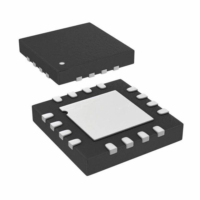
ICGOO电子元器件商城为您提供ADA4096-4ACPZ-R7由Analog设计生产,在icgoo商城现货销售,并且可以通过原厂、代理商等渠道进行代购。 ADA4096-4ACPZ-R7价格参考¥25.57-¥47.99。AnalogADA4096-4ACPZ-R7封装/规格:线性 - 放大器 - 仪表,运算放大器,缓冲器放大器, General Purpose Amplifier 4 Circuit Rail-to-Rail 16-LFCSP-WQ (3x3)。您可以下载ADA4096-4ACPZ-R7参考资料、Datasheet数据手册功能说明书,资料中有ADA4096-4ACPZ-R7 详细功能的应用电路图电压和使用方法及教程。
ADA4096-4ACPZ-R7是Analog Devices Inc.推出的一款四通道、微功耗、轨至轨输入/输出运算放大器,属于线性放大器类别,广泛应用于对功耗和精度要求较高的场合。其典型应用场景包括便携式和电池供电设备,如医疗仪器(心率监测器、血糖仪)、可穿戴设备(智能手表、健康传感器)等,得益于其低静态电流(每放大器仅45μA),可显著延长电池寿命。

该器件具有宽电源电压范围(2.2V至5.5V),适合单电源或双电源系统,适用于工业控制中的传感器信号调理电路,例如压力、温度、加速度传感器的信号放大与处理。其轨至轨输入输出特性确保在低电压下仍能最大化动态范围,提升测量精度。

此外,ADA4096-4ACPZ-R7具备良好的抗电磁干扰(EMI)能力,适用于电磁环境复杂的工业现场设备。它也常用于数据采集系统、低功耗ADC驱动、有源滤波电路以及音频信号预处理等应用中。工作温度范围为-40°C至+125°C,满足工业级环境要求。

综上,该型号因其低功耗、高稳定性和宽电压适应能力,特别适用于便携式医疗设备、工业传感、自动化控制及各类低功耗信号调理系统。
| 参数 | 数值 |
| -3db带宽 | 1.52MHz |
| 产品目录 | 集成电路 (IC) |
| 描述 | IC OPAMP GP 786KHZ RRO 16LFCSP |
| 产品分类 | Linear - Amplifiers - Instrumentation, OP Amps, Buffer Amps |
| 品牌 | Analog Devices Inc |
| 数据手册 | |
| 产品图片 | |
| 产品型号 | ADA4096-4ACPZ-R7 |
| PCN组件/产地 | |
| rohs | 无铅 / 符合限制有害物质指令(RoHS)规范要求 |
| 产品系列 | - |
| 产品培训模块 | http://www.digikey.cn/PTM/IndividualPTM.page?site=cn&lang=zhs&ptm=30008http://www.digikey.cn/PTM/IndividualPTM.page?site=cn&lang=zhs&ptm=26202 |
| 供应商器件封装 | 16-LFCSP-WQ(3x3) |
| 其它名称 | ADA4096-4ACPZ-R7CT |
| 包装 | 剪切带 (CT) |
| 压摆率 | 0.4 V/µs |
| 增益带宽积 | 786kHz |
| 安装类型 | 表面贴装 |
| 封装/外壳 | 16-WFQFN 裸露焊盘,CSP |
| 工作温度 | -40°C ~ 125°C |
| 放大器类型 | 通用 |
| 标准包装 | 1 |
| 电压-电源,单/双 (±) | 3 V ~ 30 V, ±1.5 V ~ 15 V |
| 电压-输入失调 | 35µV |
| 电流-电源 | 60µA |
| 电流-输入偏置 | 3nA |
| 电流-输出/通道 | 10mA |
| 电路数 | 4 |
| 视频文件 | http://www.digikey.cn/classic/video.aspx?PlayerID=1364138032001&width=640&height=505&videoID=2245193153001 |
| 输出类型 | 满摆幅 |


- 商务部:美国ITC正式对集成电路等产品启动337调查
- 曝三星4nm工艺存在良率问题 高通将骁龙8 Gen1或转产台积电
- 太阳诱电将投资9.5亿元在常州建新厂生产MLCC 预计2023年完工
- 英特尔发布欧洲新工厂建设计划 深化IDM 2.0 战略
- 台积电先进制程称霸业界 有大客户加持明年业绩稳了
- 达到5530亿美元!SIA预计今年全球半导体销售额将创下新高
- 英特尔拟将自动驾驶子公司Mobileye上市 估值或超500亿美元
- 三星加码芯片和SET,合并消费电子和移动部门,撤换高东真等 CEO
- 三星电子宣布重大人事变动 还合并消费电子和移动部门
- 海关总署:前11个月进口集成电路产品价值2.52万亿元 增长14.8%


PDF Datasheet 数据手册内容提取
30 V, Micropower, Overvoltage Protection, Rail-to-Rail Input/Output Amplifiers Data Sheet ADA4096-2/ADA4096-4 FEATURES PIN CONNECTION DIAGRAMS Input overvoltage protection, 32 V above and below the OUTA 1 8 V+ supply rails –INA 2 ADA4096-2 7 OUTB Nop pohwaesre s ruepvperlys al for input voltage up to ±32 V beyond the +INVA– 34 (NToOt Pto V SIEcaWle) 65 –+IINNBB 09241-001 Rail-to-rail input and output swing Figure 1. 8-Lead, MSOP (RM-8), ADA4096-2 Low power: 60 µA per amplifier typical Unity-gain bandwidth OUTA1 8V+ 800 kHz typical at VSY = ±15 V –INA2 ADA4096-2 7OUTB TOP VIEW 550 kHz typical at VSY = ±5 V +INA3 (Not to Scale) 6–INB 465 kHz typical at VSY = ±1.5 V V–4 5+INB Single-supply operation: 3 V to 30 V LLoarwg eo fsfisgenta vlo vlotaltgaeg:e 3 g00ai µnV: 1 m20a xdiBm tuympi cal N1.OCTTOOE NSVN–E.CT THE EXPOSED PAD 09241-002 Unity gain stable Figure 2. 8-Lead LFCSP (CP-8-10), ADA4096-2 Qualified for automotive applications Note: For the ADA4096-4, see the Pin Configurations and APPLICATIONS Function Descriptions section. Battery monitoring Sensor conditioners Portable power supply controls Portable instrumentation GENERAL DESCRIPTION T The ADA4096-2 dual and ADA4096-4 quad operational amplifiers feature micropower operation and rail-to-rail input and output ranges. The extremely low power requirements and guaranteed operation from 3 V to 30 V make these amplifiers perfectly suited to monitor battery usage and to control battery 1 charging. Their dynamic performance, including 27 nV/√Hz voltage noise density, recommends them for battery-powered audio applications. Capacitive loads to 200 pF are handled without oscillation. The ADA4096-2 and ADA4096-4 have overvoltage protection ianbpouvtes aanndd bdeiloodwe st hthe astu aplplolyw r tahiles ,v moltaakgien gin tphuist dtoe veixctee nidde a3l2 f oVr CH1 10.0V CH2 10.0V MT 2 . 0 304m.2s0% A CH1 –3.6V 09241-146 robust industrial applications. The ADA4096-2 and ADA4096-4 Figure 3. No Phase Reversal feature a unique input stage that allows the input voltage to The ADA4096-2 family is specified over the extended industrial exceed either supply safely without any phase reversal or latch- temperature range of (−40°C to +125°C) and is part of the up; this is called overvoltage protection, or OVP. growing selection of 30 V, low power op amps from Analog The dual ADA4096-2 is available in 8-lead LFCSP (2 mm × Devices, Inc. (see Table 1). 2 mm) and 8-lead MSOP packages. The ADA4096-2 is available Table 1. Low Power, 30 V Operational Amplifiers in 16-lead LFCSP (3 mm × 3 mm) and 14-lead TSSOP Op Amp Rail-to-Rail I/O PJFET Low Noise packages. The ADA4096-2W is qualified for automotive Dual ADA4091-2 AD8682 AD8622 applications and is available in an 8-lead MSOP package. Quad ADA4091-4 AD8684 AD8624 Rev. G Document Feedback Information furnished by Analog Devices is believed to be accurate and reliable. However, no responsibility is assumed by Analog Devices for its use, nor for any infringements of patents or other One Technology Way, P.O. Box 9106, Norwood, MA 02062-9106, U.S.A. rights of third parties that may result from its use. Specifications subject to change without notice. No license is granted by implication or otherwise under any patent or patent rights of Analog Devices. Tel: 781.329.4700 ©2011–2017 Analog Devices, Inc. All rights reserved. Trademarks and registered trademarks are the property of their respective owners. Technical Support www.analog.com
ADA4096-2/ADA4096-4 Data Sheet TABLE OF CONTENTS Features .............................................................................................. 1 ±1.5 V Characteristics ............................................................... 10 Applications ....................................................................................... 1 ±5 V Characteristics................................................................... 13 Pin Connection Diagrams ............................................................... 1 ±15 V Characteristics ................................................................ 16 General Description ......................................................................... 1 Comparative Voltage and Variable Voltage Graphs ............... 19 Revision History ............................................................................... 3 Theory of Operation ...................................................................... 20 Specifications ..................................................................................... 4 Input Stage ................................................................................... 20 Electrical Specifications, V = ±1.5 V ....................................... 4 Phase Inversion ........................................................................... 20 SY Electrical Specifications, V = ±5 V .......................................... 5 Input Overvoltage Protection ................................................... 21 SY Electrical Specifications, V = ±15 V ........................................ 6 Comparator Operation .............................................................. 21 SY Absolute Maximum Ratings ............................................................ 7 Outline Dimensions ....................................................................... 22 Thermal Resistance ...................................................................... 7 Ordering Guide .......................................................................... 24 ESD Caution .................................................................................. 7 Automotive Products ................................................................. 24 Pin Configurations and Function Descriptions ........................... 8 Typical Performance Characteristics ........................................... 10 Rev. G | Page 2 of 25
Data Sheet ADA4096-2/ADA4096-4 REVISION HISTORY 9/2017—Rev. F to Rev. G 8/2012—Rev. A to Rev. B Changed ADA409x to ADA4096-2 ............................ Throughout Added ADA4096-4 ............................................................ Universal Changed CP-16-27 to CP-16-22 .................................. Throughout Changes to Features Section ............................................................ 1 Changes to Figure 12 and Figure 13 ............................................. 10 Added Figure 3 .................................................................................. 1 Changes to Figure 26 ...................................................................... 13 Changes to Pin Connection Diagrams Section ............................. 1 Changes to Figure 39 ...................................................................... 16 Changes to Input Bias Current, Common-Mode Rejection Updated Outline Dimensions ........................................................ 22 Ratio, Large Signal Voltage Gain, and Supply Current per Changes to Ordering Guide ........................................................... 24 Amplifier Parameters, and −3 dB Closed-Loop Bandwidth Symbol, Table 2 .................................................................................. 3 12/2014—Rev. E to Rev. F Changes to Input Bias Current, Common-Mode Rejection Changes to EPAD Note, Figure 2 .................................................... 1 Ratio, Large Signal Voltage Gain, and Parameters, and −3 dB Changes to EPAD Note, Figure 5 and Table 7 ............................... 7 Closed-Loop Bandwidth Symbol, Table 3 ..................................... 4 Changes to EPAD Note, Figure 7 and Table 8 ............................... 8 Changes to Input Bias Current, Common-Mode Rejection Ratio, Large Signal Voltage Gain, Output Voltage High, and 3/2014—Rev. D to Rev. E Output Voltage Low Parameters, and −3 dB Closed-Loop Changes to Figure 10 and Figure 12 ............................................... 9 Bandwidth Symbol, Table 4 ............................................................. 5 Changes to Figure 23 and Figure 25 ............................................. 12 Changes to Table 6 ............................................................................ 7 Changes to Figure 36 and Figure 38 ............................................. 15 Added Pin Configurations and Function Descriptions Section ................................................................................................ 8 5/2013—Rev. C to Rev. D Added Figure 4 and Figure 5, Renumbered Sequentially ............ 8 Changes to Pin Connection Diagrams Section ............................. 1 Added Table 7, Renumbered Sequentially ..................................... 8 Changes to Pin Configurations and Function Descriptions Added Figure 6, Figure 7, and Table 8 ............................................ 9 Section ................................................................................................ 7 Updated Outline Dimensions........................................................ 18 Added Figure 10, Renumbered Sequentially ................................. 9 Changes to Ordering Guide ........................................................... 20 Added Figure 23 .............................................................................. 12 Added Figure 36 .............................................................................. 15 3/2012—Rev. 0 to Rev. A Changed −3 dB Closed-Loop Bandwidth from 97 kHz to 8/2012—Rev. B to Rev. C 970 kHz, Table 2 ................................................................................ 3 Changes to Table 8 ............................................................................ 8 Changed −3 dB Closed-Loop Bandwidth from 114 kHz to 1140 kHz, Table 3 .............................................................................. 4 Changed to −3 dB Closed-Loop Bandwidth from 152 kHz to 1520 kHz, Table 4 .............................................................................. 5 Updated Outline Dimensions........................................................ 18 7/2011—Revision 0: Initial Version Rev. G | Page 3 of 25
ADA4096-2/ADA4096-4 Data Sheet SPECIFICATIONS ELECTRICAL SPECIFICATIONS, V = ±1.5 V SY V = ±1.5 V, V = V /2, T = 25°C, unless otherwise noted. SY CM SY A Table 2. Parameter Symbol Test Conditions/Comments Min Typ Max Unit INPUT CHARACTERISTICS Offset Voltage V 35 300 µV OS 0°C ≤ T ≤ +125°C 450 µV A −40°C ≤ T ≤ +125°C 900 µV A Offset Voltage Drift ∆V /∆T −40°C ≤ T ≤ +125°C 1 µV/°C OS A Input Bias Current I ±10 ±25 nA B −40°C ≤ T ≤ +125°C ±30 nA A Input Offset Current I ±0.1 ±1.5 nA OS −40°C ≤ T ≤ +125°C ±3 nA A Input Voltage Range −1.5 +1.5 V Common-Mode Rejection Ratio CMRR V = 0 V to ±1.5 V 61 77 dB CM −40°C ≤ T ≤ +125°C 58 dB A Large Signal Voltage Gain A R = 10 kΩ, V = −1.4 V to +1.4 V 91 94 dB VO L O −40°C ≤ T ≤ +125°C 84 dB A R = 2 kΩ, V = −1.3 V to +1.3 V 86 92 dB L O −40°C ≤ T ≤ +125°C 77 dB A MATCHING CHARACTERISTICS Offset Voltage T = 25°C 100 300 µV A OUTPUT CHARACTERISTICS Output Voltage High V R = 10 kΩ to GND 1.48 1.49 V OH L −40°C ≤ T ≤ +125°C 1.45 V A R = 2 kΩ to GND 1.45 1.46 V L −40°C to +125°C 1.40 V Output Voltage Low V R = 10 kΩ to GND −1.49 −1.48 V OL L −40°C ≤ T ≤ +125°C −1.45 V A R = 2 kΩ to GND −1.48 −1.47 V L −40°C ≤ T ≤ +125°C −1.40 V A Short-Circuit Limit I Source/sink ±10 mA SC Closed-Loop Impedance Z f = 100 kHz, A = 1 102 Ω OUT V POWER SUPPLY Power Supply Rejection Ratio PSRR V = 3 V to 36 V 100 dB SY −40°C ≤ T ≤ +125°C 90 dB A Supply Current per Amplifier I V = V /2 40 50 µA SY O SY −40°C ≤ T ≤ +125°C 80 µA A DYNAMIC PERFORMANCE Slew Rate SR R = 100 kΩ, C = 30 pF 0.25 V/µs L L Gain Bandwidth Product GBP V = 5 mV p-p, R = 10 kΩ, A = 100 501 kHz IN L V Unity-Gain Crossover UGC V = 5 mV p-p, R = 10 kΩ, A = 1 465 kHz IN L V Phase Margin Φ 51 Degrees M −3 dB Closed-Loop Bandwidth f A = 1, V = 5 mV p-p 970 kHz −3 dB V IN NOISE PERFORMANCE Voltage Noise e p-p 0.1 Hz to 10 Hz 0.7 µV p-p n Voltage Noise Density e f = 1 kHz 27 nV/√Hz n Current Noise Density i f = 1 kHz 0.2 pA/√Hz n Rev. G | Page 4 of 25
Data Sheet ADA4096-2/ADA4096-4 ELECTRICAL SPECIFICATIONS, V = ±5 V SY V = ±5 V, V = V /2, T = 25°C, unless otherwise noted. SY CM SY A Table 3. Parameter Symbol Test Conditions/Comments Min Typ Max Unit INPUT CHARACTERISTICS Offset Voltage V 35 300 µV OS −40°C ≤ T ≤ +125°C 500 µV A Offset Voltage Drift ∆V /∆T 1 µV/°C OS Input Bias Current I ±10 ±25 nA B −40°C ≤ T ≤ +125°C ±30 nA A Input Offset Current I ±1.5 ±2 nA OS −40°C ≤ T ≤ +125°C ±3 nA A Input Voltage Range −5 +5 V Common-Mode Rejection Ratio CMRR V = −5 V to +5 V 72 86 dB CM −40°C ≤ T ≤ +125°C 68 dB A V = −3 V to +3 V 91 103 dB CM −40°C ≤ T ≤ +125°C 85 dB A Large Signal Voltage Gain A R = 10 kΩ, V = ±4.8 V 102 111 dB VO L O −40°C ≤ T ≤ +125°C 99 dB A R = 2 kΩ, V = ±4.7 V 93 103 dB L O −40°C ≤ T ≤ +125°C 88 dB A MATCHING CHARACTERISTICS Offset Voltage T = 25°C 100 300 µV A OUTPUT CHARACTERISTICS Output Voltage High V R = 10 kΩ to GND 4.96 4.97 V OH L −40°C ≤ T ≤ +125°C 4.95 V A R = 2 kΩ to GND 4.80 4.90 V L −40°C ≤ T ≤ +125°C 4.70 V A Output Voltage Low V R = 10 kΩ to GND −4.98 −4.97 V OL L −40°C ≤ T ≤ +125°C −4.95 V A R = 2 kΩ to GND −4.90 −4.80 V L −40°C ≤ T ≤ +125°C −4.75 V A Short-Circuit Limit I Source/sink ±10 mA SC Closed-Loop Impedance Z f = 100 kHz, A = 1 71 Ω OUT V POWER SUPPLY Power Supply Rejection Ratio PSRR V = 3 V to 36 V 100 dB SY −40°C ≤ T ≤ +125°C 90 dB A Supply Current per Amplifier I V = V /2 47 55 µA SY O SY −40°C ≤ T ≤ +125°C 75 µA A DYNAMIC PERFORMANCE Slew Rate SR R = 100 kΩ, C = 30 pF 0.3 V/µs L L Gain Bandwidth Product GBP V = 5 mV p-p, R = 10 kΩ, A = 100 595 kHz IN L V Unity-Gain Crossover UGC V = 5 mV p-p, R = 10 kΩ, A = 1 550 kHz IN L V Phase Margin Φ 52 Degrees M −3 dB Closed-Loop Bandwidth f A = 1, V = 5 mV p-p 1140 kHz −3 dB V IN NOISE PERFORMANCE Voltage Noise e p-p 0.1 Hz to 10 Hz 0.7 µV p-p n Voltage Noise Density e f = 1 kHz 27 nV/√Hz n Current Noise Density i f = 1 kHz 0.2 pA/√Hz n Rev. G | Page 5 of 25
ADA4096-2/ADA4096-4 Data Sheet ELECTRICAL SPECIFICATIONS, V = ±15 V SY V = ±15 V, V = V /2, V = 0.0 V, T = 25°C, unless otherwise noted. SY CM SY O A Table 4. Parameter Symbol Test Conditions/Comments Min Typ Max Unit INPUT CHARACTERISTICS Offset Voltage V 35 300 µV OS −40°C ≤ T ≤ +125°C 500 µV A Offset Voltage Drift ∆V /∆T 1 µV/°C OS Input Bias Current I ±3 ±25 nA B −40°C ≤ T ≤ +125°C ±30 nA A Input Offset Current I ±0.1 ±1.5 nA OS −40°C ≤ T ≤ +125°C ±3 nA A Input Voltage Range −15 +15 V Common-Mode Rejection Ratio CMRR V = −15 V to +15 V 81 95 dB CM −40°C ≤ T ≤ +125°C 75 dB A V = −13 V to +13 V 95 107 dB CM −40°C ≤ T ≤ +125°C 89 dB A Large Signal Voltage Gain A R = 10 kΩ, V = ±14.7 V 109 120 dB VO L O −40°C ≤ T ≤ +125°C 105 dB A R = 2 kΩ, V = ±11 V 99 112 dB L O −40°C ≤ T ≤ +125°C 90 dB A Input Capacitance Differential Mode C 2.5 pF DM Common Mode C 7 pF CM MATCHING CHARACTERISTICS Offset Voltage T = 25°C 100 300 µV A OUTPUT CHARACTERISTICS Output Voltage High V R = 10 kΩ to GND 14.92 14.94 V OH L −40°C ≤ T ≤ +125°C 14.90 V A R = 2 kΩ to GND 14.0 14.3 V L −40°C ≤ T ≤ +125°C 11.0 V A Output Voltage Low V R = 10 kΩ to GND −14.96 −14.80 V OL L −40°C ≤ T ≤ +125°C −14.75 V A R = 2 kΩ to GND −14.75 −14.60 V L −40°C ≤ T ≤ +125°C −14.0 V A Short-Circuit Limit I Source/sink ±10 mA SC Closed-Loop Impedance Z f = 100 kHz, A = 1 40 Ω OUT V POWER SUPPLY Power Supply Rejection Ratio PSRR V = 3 V to 36 V 100 dB SY −40°C ≤ T ≤ +125°C 90 dB A Supply Current per Amplifier I V = V /2 60 75 µA SY O SY −40°C ≤ T ≤ +125°C 100 µA A DYNAMIC PERFORMANCE Slew Rate SR R = 100 kΩ, C = 30 pF 0.4 V/µ L L Settling Time t To 0.1%, 10 V step 23.4 µs S Gain Bandwidth Product GBP V = 5 mV p-p, R = 10 kΩ, A = 100 786 kHz IN L V Unity-Gain Crossover UGC V = 5 mV p-p, R = 10 kΩ, A = 1 800 kHz IN L V Phase Margin Φ 60 Degrees M −3 dB Closed-Loop Bandwidth f A = 1, V = 5 mV p-p 1520 kHz −3 dB V IN Channel Separation CS f = 1 kHz 100 dB NOISE PERFORMANCE Voltage Noise e p-p 0.1 Hz to 10 Hz 0.7 µV p-p n Voltage Noise Density e f = 1 kHz 27 nV/√Hz n Current Noise Density i f = 1 kHz 0.2 pA/√Hz n Rev. G | Page 6 of 25
Data Sheet ADA4096-2/ADA4096-4 ABSOLUTE MAXIMUM RATINGS THERMAL RESISTANCE Table 5. Parameter Rating θ is specified for the device soldered on a 4-layer JEDEC JA Supply Voltage 36 V standard printed circuit board (PCB) with zero airflow. The Input Voltage exposed pad is soldered to the application board. Operating Condition −V ≤ V ≤ +V IN Table 6. Thermal Resistance Overvoltage Condition1 (−V) − 32 V ≤ V ≤ (+V) + 32 V IN Package Type θ θ Unit Differential Input Voltage2 ±V JA JC SY 8-Lead MSOP (RM-8) 142 45 °C/W Input Current ±5 mA 8-Lead LFCSP (CP-8-10) 76 43 °C/W Output Short-Circuit Duration to Indefinite GND 14-Lead TSSOP (RU-14) 112 35 °C/W Storage Temperature Range −65°C to +150°C 16-Lead LFCSP (CP-16-22) 75 12 °C/W Operating Temperature Range −40°C to +125°C Junction Temperature Range −65°C to +150°C ESD CAUTION Lead Temperature (Soldering, 300°C 60 seconds) 1 Performance not guaranteed during overvoltage conditions. 2 Limit the input current to ±5 mA. Stresses at or above those listed under Absolute Maximum Ratings may cause permanent damage to the product. This is a stress rating only; functional operation of the product at these or any other conditions above those indicated in the operational section of this specification is not implied. Operation beyond the maximum operating conditions for extended periods may affect product reliability. Rev. G | Page 7 of 25
ADA4096-2/ADA4096-4 Data Sheet PIN CONFIGURATIONS AND FUNCTION DESCRIPTIONS OUTA 1 8 V+ OUTA1 8V+ –INA 2 ADA4096-2 7 OUTB –INA2 ADA4096-2 7OUTB +INVA– 34 (NToOt Pto V SIEcaWle) 65 –+IINNBB 09241-201 +INVA–34 (NToOt Pto V SIEcaWle) 65–+IINNBB N1.OCTTOOE NSVN–E.CT THE EXPOSED PAD 09241-202 Figure 4. 8-Lead, MSOP (RM-8), ADA4096-2 Figure 5. 8-Lead LFCSP (CP-8-10), ADA4096-2 Table 7. Pin Function Descriptions, ADA4096-2 Pin No.1 8-Lead MSOP 8-Lead LFCSP Mnemonic Description 1 1 OUTA Output Channel A. 2 2 −INA Negative Input Channel A. 3 3 +INA Positive Input Channel A. 4 4 V− Negative Supply Voltage. 5 5 +INB Positive Input Channel B. 6 6 −INB Negative Input Channel B. 7 7 OUTB Output Channel B. 8 8 V+ Positive Supply Voltage. N/A EP2 EPAD Exposed Pad.2 For the ADA4096-2 (8-lead LFCSP only), connect the exposed pad to V−. 1 N/A means not applicable. 2 The exposed pad is not shown in the pin configuration diagram. Rev. G | Page 8 of 25
Data Sheet ADA4096-2/ADA4096-4 A D CNI TUO TUO CNI 6 5 4 3 1 1 1 1 OUTA 1 14 OUTD –INA 1 12 –IND –INA 2 13 –IND +INA 2 ADA4096-4 11 +IND +INA 3 ADA4096-4 12 +IND V+ 3 VTIOEWP 10 V– V+ 4 (NToOt Pto V SIEcaWle) 11 V– +INB 4 9 +INC +INB 5 10 +INC –INB 6 9 –INC 5 6 7 8 OUTB 7 8 OUTC 09241-101 BN–I BTUO CTUO CNI– 21N..O NCTIOCEN S=N NEOCTT TINHTEE ERXNPAOLLSYE DC OPANDN ETCOT VE–D.. 09241-103 Figure 6. 14-Lead TSSOP (RU-14), ADA4096-4 Figure 7. 16-Lead LFCSP (CP-16-22), ADA4096-4 Table 8. Pin Function Descriptions, ADA4096-4 Pin No.1 14-Lead TSSOP 16-Lead LFCSP Mnemonic Description 1 15 OUTA Output Channel A. 2 1 −INA Negative Input Channel A. 3 2 +INA Positive Input Channel A. 4 3 V+ Positive Supply Voltage. 5 4 +INB Positive Input Channel B. 6 5 −INB Negative Input Channel B. 7 6 OUTB Output Channel B. 8 7 OUTC Output Channel C. 9 8 −INC Negative Input Channel C. 10 9 +INC Positive Input Channel C. 11 10 V− Negative Supply Voltage. 12 11 +IND Positive Input Channel D. 13 12 −IND Negative Input Channel D. 14 14 OUTD Output Channel D. N/A 13 NIC No Internal Connection. N/A 16 NIC No Internal Connection. N/A EP2 EPAD Exposed Pad.2 For the ADA4096-4 (16-lead LFCSP only), connect the exposed pad to V−. 1 N/A means not applicable. 2 The exposed pad is not shown in the pin configuration diagram. Rev. G | Page 9 of 25
ADA4096-2/ADA4096-4 Data Sheet TYPICAL PERFORMANCE CHARACTERISTICS T = 25°C, unless otherwise noted. All typical performance characteristics shown are for the ADA4096-2 only. A ±1.5 V CHARACTERISTICS 180 30 ADA4096-2 ADA4096-2 160 VSY = ±1.5V VSY = ±1.5V TA = 25°C 20 140 S R 10 E LIFI 120 TA = +25°C TA = +125°C R OF AMP 10800 I (nA)B –100 TA = +85°C E MB 60 TA = 0°C U –20 N 40 –30 20 TA = –40°C 0 –40 –200 –175 –150 –125 –100 –75 –50 –25VO0S (µ25V)50 75 100 125 150 175 200 MORE 09241-003 –1.5 –1.0 –0.5 VCM0 (V) 0.5 1.0 1.5 09241-005 Figure 8. Input Offset Voltage (VOS) Distribution Figure 11. Input Bias Current (IB) vs. VCM for Various Temperatures 25 10k ADA4096-2 ADA4096-2 VSY = ±1.5V mV) VSY = ±1.5V 20 TA = –40°C TO +125°C AIL ( TA = 25°C S R 1k FIER PLY AMPLI 15 O SUP OF E T 100 MBER 10 OLTAG SOURCING U V N T 10 SINKING 5 PU T U O 0–2.5 –2.0 –1.5 –1.0 –0T.5CVOS0 (µV/0°.C5) 1.0 1.5 2.0 2.5 09241-004 01.001 0.01 LOAD CU0R.1RENT (mA) 1 10 09241-006 Figure 9. Offset Voltage Drift (TCVOS) Distribution Figure 12. Output Voltage to Supply Rail vs. Load Current 800 100 225 ADA4096-2 600 80 TVASY = = 2 5±°1C.5V 180 400 60 135 200 40 90 es) V (µV)OS –2000 GAIN (dB) 200 GAIN PHASE 045 HASE (Degre P –400 –20 –45 ––860000–1.5 –1.3 –1.0 –01V.08S YC– =H0A.±51N.–N50VE.3LVSCM0 (V)0.3 0.5 0.8 1.0 1.3 1.509241-210 ––4600100 1k F1R0EkQUENCY1 (0H0zk) 1M 10M––19305 09241-007 Figure 10. Input Offset Voltage (VOS) vs. Common-Mode Voltage (VCM) Figure 13. Open-Loop Gain and Phase vs. Frequency Rev. G | Page 10 of 25
Data Sheet ADA4096-2/ADA4096-4 50 120 G = +100 ADA4096-2 ADA4096-2 40 VSY = ±1.5V VSY = ±1.5V TA = 25°C 100 TA = 25°C 30 B) G = +10 d 20 80 N ( PSRR+ GAI 10 B) 60 OOP 0 G = +1 RR (d PSRR– D-L–10 PS 40 E S LO–20 20 C –30 0 –40 –5010 100 1kFREQU1E0NkCY (Hz1)00k 1M 10M 09241-008 –2010 100 1kFREQU1E0NkCY (Hz1)00k 1M 10M 09241-052 Figure 14. Closed-Loop Gain vs. Frequency Figure 16. PSRR vs. Frequency 10k 2.0 ADA4096-2 ADA4096-2 1k TVASY = = 2 5±°1C.5V 1.5 TVASY = = 2 5±°1C.5V RL = 10kΩ 1.0 CL = 100pF G = +1 100 0.5 Ω) G = +100 V) (UT 10 (UT 0 O O Z G = +10 V –0.5 1 –1.0 G = +1 0.1 –1.5 0.0110 100 1kFREQU1E0NkCY (Hz1)00k 1M 10M 09241-009 –2.00 20 40 TIM6E0 (µs) 80 100 120 09241-010 Figure 15. Output Impedance (ZOUT) vs. Frequency Figure 17. Large Signal Transient Response Rev. G | Page 11 of 25
ADA4096-2/ADA4096-4 Data Sheet 0.08 0.2 ADA4096-2 ADA4096-2 0.06 VSY = ±1.5V 0 VSY = ±1.5V TA = 25°C TA = 25°C 0.04 RCLL == 1100k0ΩpF –0.2 RRFS == 1100k0ΩΩ G = +1 0.02 –0.4 V) 0 V) –0.6 (UT (UT VO–0.02 VO –0.8 –0.04 –1.0 –0.06 –1.2 –0.08 –1.4 –0.100 5 10 TIM1E5 (µs) 20 25 30 09241-011 –1.60 20 40TIME (µs)60 80 100 09241-056 Figure 18. Small Signal Transient Response Figure 20. Negative Overload Recovery 1.6 ADA4096-2 1.4 VTASY = = 2 5±°1C.5V RF = 10kΩ 1.2 RS = 100Ω 1.0 V) (UT 0.8 O V 0.6 0.4 0.2 00 20 40TIME (µs)60 80 100 09241-055 Figure 19. Positive Overload Recovery Rev. G | Page 12 of 25
Data Sheet ADA4096-2/ADA4096-4 ±5 V CHARACTERISTICS 250 30 ADA4096-2 ADA4096-2 TVASY = = 2 5±°5CV 20 VSY = ±5V 200 S 10 ER TA = +125°C FI PLI 150 0 TA = +85°C OF AM (nA)B –10 R 100 I E –20 B M NU –30 TA = +25°C 50 TA = 0°C –40 TA = –40°C 0 –50 –200 –175 –150 –125 –100 –75 –50 –25VO0S (µ25V)50 75 100 125 150 175 200 MORE 09241-015 –5 –4 –3 –2 –1 VCM0 (V) 1 2 3 4 5 09241-050 Figure 21. Input Offset Voltage (VOS) Distribution Figure 24. Input Bias Current (IB) vs. VCM for Various Temperatures 40 10k ADA4096-2 ADA4096-2 35 TVASY = = – 4±05°VC TO +125°C L (mV) TVASY = = 2 5±°5CV AI S 30 R 1k FIER PLY OF AMPLI 2205 E TO SUP 100 MBER 15 OLTAG SOURCING NU 10 T V 10 SINKING U P T 5 U O 0–2.5 –2.0 –1.5 –1.0 –0T.5CVOS0 (µV/0°.C5) 1.0 1.5 2.0 2.5 09241-016 01.001 0.01 LOA0.D1 CURRENT1 (mA) 10 100 09241-023 Figure 22. Offset Voltage Drift (TCVOS) Distribution Figure 25. Output Voltage to Supply Rail vs. Load Current 800 100 225 ADA4096-2 600 V10S YC =HA±5NVNELS 80 VTASY = = 2 5±°5CV 180 400 60 135 200 40 90 es) V (µV)OS –2000 GAIN (dB) 200 GAIN PHASE 045 HASE (Degre P –400 –20 –45 ––860000–5 –4 –3 –2 –1 VCM0 (V) 1 2 3 4 509241-223 ––4600100 1k F1R0EkQUENCY1 (0H0zk) 1M 10M––19305 09241-020 Figure 23. Input Offset Voltage (VOS) vs. Common-Mode Voltage (VCM) Figure 26. Open-Loop Gain and Phase vs. Frequency Rev. G | Page 13 of 25
ADA4096-2/ADA4096-4 Data Sheet 50 140 G = +100 ADA4096-2 ADA4096-2 40 TVASY = = 2 5±°5CV 120 TVASY = = 2 5±°5CV 30 B) G = +10 100 d 20 N ( GAI 10 B) 80 PSRR+ OP 0 G = +1 R (d 60 O R D-L–10 PS PSRR– E 40 S LO–20 C 20 –30 0 –40 –5010 100 1kFREQU1E0NkCY (Hz1)00k 1M 10M 09241-024 –2010 100 1kFREQU1E0NkCY (Hz1)00k 1M 10M 09241-053 Figure 27. Closed-Loop Gain vs. Frequency Figure 29. PSRR vs. Frequency 10k 6 ADA4096-2 ADA4096-2 VSY = ±5V VSY = ±5V 1k TA = 25°C 4 TA = 25°C RL = 10kΩ CL = 100pF G = +1 100 2 Ω) G = +100 V) (UT 10 (UT 0 O O Z V G = +10 1 –2 G = +1 0.1 –4 0.0110 100 1kFREQU1E0NkCY (Hz1)00k 1M 10M 09241-021 –60 50 100 150 TIM2E0 0(µs) 250 300 350 400 09241-017 Figure 28. Output Impedance (ZOUT) vs. Frequency. Figure 30. Large Signal Transient Response Rev. G | Page 14 of 25
Data Sheet ADA4096-2/ADA4096-4 0.08 1 ADA4096-2 ADA4096-2 0.06 VSY = ±5V VSY = ±5V TA = 25°C 0 TA = 25°C 0.04 RCLL == 1100k0ΩpF RRFS == 1100k0ΩΩ G = +1 0.02 –1 V) 0 V) (UT (UT –2 VO–0.02 VO –0.04 –3 –0.06 –4 –0.08 –0.100 5 10 TIM1E5 (µs) 20 25 30 09241-018 –50 20 40TIME (µs)60 80 100 09241-058 Figure 31. Small Signal Transient Response Figure 33. Negative Overload Recovery 6 ADA4096-2 VSY = ±5V 5 TA = 25°C RF = 10kΩ RS = 100Ω 4 V) (UT 3 O V 2 1 00 20 40TIME (µs)60 80 100 09241-057 Figure 32. Positive Overload Recovery Rev. G | Page 15 of 25
ADA4096-2/ADA4096-4 Data Sheet ±15 V CHARACTERISTICS 250 40 ADA4096-2 ADA4096-2 VSY = ±15V 30 VSY = ±15V TA = 25°C 200 20 ERS 10 TA = +85°C TA = +125°C FI PLI 150 0 OF AM (nA)B –10 R 100 I –20 BE TA = +25°C UM –30 TA = 0°C N 50 –40 –50 TA = –40°C 0 –60 –200 –175 –150 –125 –100 –75 –50 –25VO0S (µ25V)50 75 100 125 150 175 200 MORE 09241-027 –15 –10 –5 VCM0 (V) 5 10 15 09241-051 Figure 34. Input Offset Voltage (VOS) Distribution Figure 37. Input Bias Current (IB) vs. VCM for Various Temperatures 35 10k ADA4096-2 ADA4096-2 30 TVASY = = – 4±01°5CV TO +125°C L (mV) TVASY = = 2 5±°1C5V AI S R 1k FIER 25 PLY MPLI 20 SUP A O OF E T 100 MBER 15 OLTAG SOURCING NU 10 T V 10 SINKING U P 5 UT O 0–2.5 –2.0 –1.5 –1.0 –0T.5CVOS0 (µV/0°.C5) 1.0 1.5 2.0 2.5 09241-028 01.001 0.01 LOA0.D1 CURRENT1 (mA) 10 100 09241-034 Figure 35. Offset Voltage Drift (TCVOS) Distribution Figure 38. Output Voltage to Supply Rail vs. Load Current 800 100 225 ADA4096-2 600 1V0S YC =HA±1N5NVELS 80 VTASY = = 2 5±°1C5V 180 400 60 135 200 40 90 es) V (µV)OS 0 GAIN (dB) 20 GAIN PHASE 45 ASE (Degre –200 0 0 H P –400 –20 –45 ––860000–15 –12 –9 –6 –3 VCM0 (V) 3 6 9 12 1509241-236 ––4600100 1k F1R0EkQUENCY1 (0H0zk) 1M 10M––19305 09241-030 Figure 36. Input Offset Voltage (VOS) vs. Common-Mode Voltage (VCM) Figure 39. Open-Loop Gain and Phase vs. Frequency Rev. G | Page 16 of 25
Data Sheet ADA4096-2/ADA4096-4 50 120 ADA4096-2 ADA4096-2 G = +100 40 VSY = ±15V VSY = ±15V TA = 25°C 100 TA = 25°C 30 B) d G = +10 80 N ( 20 PSRR+ OOP GAI 10 G = +1 RR (dB) 60 PSRR– D-L 0 PS 40 E OS–10 L 20 C –20 0 –30 –4010 100 1kFREQU1E0NkCY (Hz1)00k 1M 10M 09241-036 –2010 100 1kFREQU1E0NkCY (Hz1)00k 1M 10M 09241-054 Figure 40. Closed-Loop Gain vs. Frequency Figure 42. PSRR vs. Frequency 10k 15 ADA4096-2 ADA4096-2 VSY = ±15V VSY = ±15V 1k TA = 25°C 10 TA = 25°C RL = 10kΩ CL = 100pF G = +1 100 5 Ω) V) (UT 10 G = +100 (UT 0 O O Z V G = +10 1 –5 G = +1 0.1 –10 0.0110 100 1kFREQU1E0NkCY (Hz1)00k 1M 10M 09241-035 –150 50 100 150 TIM2E0 0(µs) 250 300 350 400 09241-031 Figure 41. Output Impedance (ZOUT) vs. Frequency Figure 43. Large Signal Transient Response Rev. G | Page 17 of 25
ADA4096-2/ADA4096-4 Data Sheet 0.08 0 ADA4096-2 ADA4096-2 0.06 VTASY = = 2 5±°1C5V –2 VTASY = = 2 5±°1C5V 0.04 RCLL == 1100k0ΩpF –4 RRFS == 1100k0ΩΩ G = +1 0.02 –6 V) 0 V) (UT (UT –8 VO–0.02 VO –10 –0.04 –12 –0.06 –0.08 –14 –0.100 5 10 TIM1E5 (µs) 20 25 30 09241-032 –160 20 40TIME (µs)60 80 100 09241-060 Figure 44. Small Signal Transient Response Figure 46. Negative Overload Recovery 16 ADA4096-2 14 VTASY = = 2 5±°1C5V RF = 10kΩ 12 RS = 100Ω 10 V) (UT 8 O V 6 4 2 00 20 40TIME (µs)60 80 100 09241-059 Figure 45. Positive Overload Recovery Rev. G | Page 18 of 25
Data Sheet ADA4096-2/ADA4096-4 COMPARATIVE VOLTAGE AND VARIABLE VOLTAGE GRAPHS 0.5 70 ADA4096-2 ADA4096-2 0.4 VTASY = = 2 5±°1C5V R (µA) 60 TRAL == ∞25°C 0.3 E LIFI 50 0.2 P M µV) 0.1 R A 40 E ( PE OIS 0 NT 30 N E R –0.1 UR C 20 Y –0.2 L P P U 10 –0.3 S –0.4–10 –8 –6 –4 –2 TIM0E (s) 2 4 6 8 10 09241-039 00 4 8 1S2UPPL1Y6 VOLT20AGE (2V4) 28 32 36 09241-043 Figure 47. Input Voltage Noise, 0.1 Hz to 10 Hz Bandwidth Figure 50. Supply Current per Amplifier vs. Supply Voltage –80 100 ADA4096-2 ADA4096-2 VSY = ±15V VSY = ±15V –90 TA = 25°C TA = 25°C B) d ON ( –100 L SEPARATI –110 e (nV/ Hz)n E 10kΩ N –120 N 1kΩ A H C –130 2kΩ VIN = 10V p-p –14020 100 FREQUE1kNCY (Hz) 10k 50k 09241-040 100.1 1 FREQUE10NCY (Hz) 100 1k 09241-044 Figure 48. Channel Separation vs. Frequency Figure 51. Voltage Noise Density (eN) vs. Frequency 120 50 ADA4096-2 ADA4096-2 110 TA = 25°C VSY = ±15V TA = 25°C 100 40 RL = 2kΩ G = +1 90 VIN = 100mV p-p VSY = ±15V %) B) 80 T ( 30 MRR (d 70 VSY = ±V1.S5YV = ±5V RSHOO C 60 E 20 OV OS– 50 40 10 OS+ 30 20100 1k F1R0EkQUENCY1 (0H0zk) 1M 10M 09241-041 00.01 CLO0A.D1 (nF) 1 09241-100 Figure 49. CMRR vs. Frequency Figure 52. Overshoot vs. Load Capacitance (CLOAD) Rev. G | Page 19 of 25
ADA4096-2/ADA4096-4 Data Sheet THEORY OF OPERATION INPUT STAGE VCC R1 R2 R5 R7 I1 I3 D6 D10 Q20 Q5 Q6 Q11 Q12 D3 C2 D9 Q18 Q3 Q4 OUT Q13 Q14 D4 Q7 Q8 C1 Q9 Q10 D8 Q17 ×1 Q19 +IN OVP Q1 Q2 R6 D2 I2 Q16 V–EINE OVP D1 R3 R4 Q15 D7 D11 09241-045 Figure 53. Simplified Schematic, ADA4096-2 Figure 53 shows a simplified schematic of the ADA4096-2. The Although phase inversion persists for only as long as the inputs input stage comprises two differential pairs (Q1 to Q4 and Q5 are saturated, it can be detrimental to applications where the to Q8) operating in parallel. When the input common-mode amplifier is part of a closed-loop system. The ADA4096-2 family voltage approaches VCC − 1.5 V, Q1 to Q4 shut down as I1 is free from phase inversion over the entire common-mode reaches its minimum voltage compliance. Conversely, when the voltage range, as well as the overvoltage protected range that is input common-mode voltage approaches V + 1.5 V, Q5 to Q8 stated in the Absolute Maximum Ratings section, Table 5. EE shut down as I2 reaches its minimum voltage compliance. This Figure 54 shows the ADA4096-2 in a unity-gain configuration topology allows for maximum input dynamic range because the with the input signal at ±40 V and the amplifier supplies at amplifier can function with its inputs at 200 mV outside the rail ±10 V. (at room temperature). T As with any rail-to-rail input amplifier, V mismatch between OS the two input pairs determines the CMRR of the amplifier. If the input common-mode voltage range is kept within 1.5 V of each rail, transitions between the input pairs are avoided, thus improving the CMRR by approximately 10 dB (see Table 3 and Table 4). 1 PHASE INVERSION Some single-supply amplifiers exhibit phase inversion when the input signal extends beyond the common-mode voltage range of the amplifier. When the input devices become saturated, the inverting and noninverting inputs exchange functions, causing the output to move in the opposing CH1 10.0V CH2 10.0V MT 2 . 0 304m.2s0% A CH1 –3.6V 09241-046 direction. Figure 54. No Phase Reversal Rev. G | Page 20 of 25
Data Sheet ADA4096-2/ADA4096-4 INPUT OVERVOLTAGE PROTECTION Note that Figure 55 represents input protection under abnormal conditions only. The correct amplifier operation input voltage The ADA4096-2 family inputs are protected from input voltage range (IVR) is specified in Table 2 to Table 4. excursions up to 32 V outside each rail. This feature is of particular importance in applications with power supply COMPARATOR OPERATION sequencing issues that could cause the signal source to be active Although op amps are quite different from comparators, before the power supplies. occasionally an unused section of a dual or a quad op amp may Figure 55 shows the input current limiting capability of the be pressed into service as a comparator; however, this is not ADA4096-2 (green curves) compared to using a 5 kΩ series recommended for any rail-to-rail output op amps. For rail-to- resistor (red curves). rail output op amps, the output stage is generally a ratioed current mirror with bipolar or metal-oxide semiconductor 7 V V A) 456 V = –15EE V = 0VEE V = +15CC foriapetleidon-e eldof fomepci,tr tr(hoMer OstoeSc FcolEnoTsde) s ttthraaegn els oiinostcpor,r ebsa.us Wte siti ttchhae nt hcnueo rdtr,ee wvnithc diec rhoivp reee rstaout littnhs gei n in m 3 NT ( 2 an increase in supply current. With the op amp configured as a E comparator, the supply current can be significantly higher (see R 1 R CU 0 Figure 56). AS –1 500 T BI –2 INPU ––43 R (µA) 400 E ––65 LOW RDSON SERIES FET PLIFI VOUT = HIGH –7 –48F–i4g0ur–e3 525.– I2n4pu–1t 6Cu–rr8eVnINt0 L(Vim)i8t5inkΩg1 6CSEaRp2Ia4EbSi lR3it2EyS I4S0TOR48 09241-047 RENT PER AM 320000 VOUT = LOW R U Figure 55 was generated with the ADA4096-2 in a buffer Y C configuration with the supplies connected to GND (or ±15 V) PL 100 P U BUFFER and the positive input swept until it exceeds the supplies by S u3p2no sdViet.i rIvvneo goltevanegreevr caooll,tn aidngipet uicoto ncnsud. rFirtoeionrn te sxi saa nlmimdp 2liet0e, 0da tµt oaAn 1 d omuvreAirn vdgo unltreainggaget oivfe 2 0 V, 00 4 8 1S2UPPL1Y6 VOLT20AGE (2V4) 28 32 36 09241-048 Figure 56. Comparator Supply Current the ADA4096-2 input current is limited to 1 mA, providing a current-limit equivalent to a series 20 kΩ resistor. Figure 55 also shows that the current limiting circuitry is active whether the amplifier is powered or not. Rev. G | Page 21 of 25
ADA4096-2/ADA4096-4 Data Sheet OUTLINE DIMENSIONS 3.20 3.00 2.80 8 5 5.15 3.20 4.90 3.00 4.65 2.80 1 4 PIN 1 IDENTIFIER 0.65 BSC 0.95 15° MAX 0.85 1.10 MAX 0.75 0.80 0.15 0.40 6° 0.23 0.55 CO0P.0L50A.1N0ARICTOYMPLIANT0. 2T5O JEDEC STA0°NDARDS 0M.0O9-187-AA 0.40 10-07-2009-B Figure 57. 8-Lead Mini Small Outline Package [MSOP] (RM-8) Dimensions shown in millimeters DETAIL A (JEDEC 95) 1.70 2.10 1.60 2.00 SQ 1.50 1.90 0.50 BSC 0.15 REF 5 8 PIN 1 INDEX 1.10 AREA EXPOSED 1.00 PAD 0.425 0.90 0.350 0.275 4 11 TOP VIEW BOTTOM VIEW PIN 1 INDICATOR AREA OPTIONS (SEE DETAIL A) 0.60 0.55 SIDE VIEW 0.05 MAX FOR PROPER CONNECTION OF 0.50 0.02 NOM THE EXPOSED PAD, REFER TO THE PIN CONFIGURATION AND FUNCTION DESCRIPTIONS PKG-003580 SEPALTAINNGE 000...322050 0.20 REF SECTION OF THIS DATA SHEET 02-08-2017-C Figure 58. 8-Lead Lead Frame Chip Scale Package [LFCSP] 2 mm × 2 mm Body and 0.55 mm Package Height (CP-8-10) Dimensions shown in millimeters Rev. G | Page 22 of 25
Data Sheet ADA4096-2/ADA4096-4 5.10 5.00 4.90 14 8 4.50 4.40 6.40 BSC 4.30 1 7 PIN 1 0.65 BSC 1.05 1.00 1M.A20X 0.20 0.80 0.09 0.75 0.15 8° 0.60 0.05 0.30 SPLEAATNIENG 0° 0.45 COPLANARITY 0.19 0.10 COMPLIANT TO JEDEC STANDARDS MO-153-AB-1 061908-A Figure 59. 14-Lead Thin Shrink Small Outline Package [TSSOP] (RU-14) Dimensions shown in millimeters DETAIL A 3.10 0.30 (JEDEC 95) 3.00 SQ 0.23 PIN 1 2.90 0.18 INDICATOR 0.50 13 16 PI(NSIENDE I 1DCAETTAOILR A A)REA OPTIONS BSC 12 1 1.75 EXPPAODSED 1.60 SQ 1.45 9 4 0.50 8 5 0.20 MIN TOP VIEW 0.40 BOTTOM VIEW 0.30 0.80 FOR PROPER CONNECTION OF 0.75 TOP VIEW THE EXPOSED PAD, REFER TO 0.05 MAX THE PIN CONFIGURATION AND 0.70 0.02 NOM FUNCTION DESCRIPTIONS COPLANARITY SECTION OF THIS DATA SHEET. SEATING 0.08 PLANE 0.20 REF PKG-005138 COMPLIANTTOJEDEC STANDARDS MO-220-WEED-6. 02-23-2017-E Figure 60. 16-Lead Lead Frame Chip Scale Package [LFCSP] 3 mm × 3 mm Body and 0.75 mm Package Height (CP-16-22) Dimensions shown in millimeters Rev. G | Page 23 of 25
ADA4096-2/ADA4096-4 Data Sheet ORDERING GUIDE Model1, 2 Temperature Range Package Description Package Option Branding ADA4096-2ARMZ −40°C to +125°C 8-Lead Mini Small Outline Package [MSOP] RM-8 A2T ADA4096-2ARMZ-R7 −40°C to +125°C 8-Lead Mini Small Outline Package [MSOP] RM-8 A2T ADA4096-2ARMZ-RL −40°C to +125°C 8-Lead Mini Small Outline Package [MSOP] RM-8 A2T ADA4096-2ACPZ-R7 −40°C to +125°C 8-Lead Lead Frame Chip Scale Package [LFCSP_UD] CP-8-10 A4 ADA4096-2ACPZ-RL −40°C to +125°C 8-Lead Lead Frame Chip Scale Package [LFCSP_UD] CP-8-10 A4 ADA4096-2WARMZ-R7 −40°C to +125°C 8-Lead Mini Small Outline Package [MSOP] RM-8 A2T ADA4096-2WARMZ-RL −40°C to +125°C 8-Lead Mini Small Outline Package [MSOP] RM-8 A2T ADA4096-4ARUZ −40°C to +125°C 14-Lead Thin Shrink Small Outline Package [TSSOP] RU-14 ADA4096-4ARUZ-R7 −40°C to +125°C 14-Lead Thin Shrink Small Outline Package [TSSOP] RU-14 ADA4096-4ARUZ-RL −40°C to +125°C 14-Lead Thin Shrink Small Outline Package [TSSOP] RU-14 ADA4096-4ACPZ-R7 −40°C to +125°C 16-Lead Lead Frame Chip Scale Package [LFCSP_WQ] CP-16-22 A30 ADA4096-4ACPZ-RL −40°C to +125°C 16-Lead Lead Frame Chip Scale Package [LFCSP_WQ] CP-16-22 A30 1 Z = RoHS Compliant Part. 2 W = Qualified for Automotive Applications. AUTOMOTIVE PRODUCTS The ADA4096-2W models are available with controlled manufacturing to support the quality and reliability requirements of automotive applications. Note that these automotive models may have specifications that differ from the commercial models; therefore, designers should review the Specifications section of this data sheet carefully. Only the automotive grade products shown are available for use in automotive applications. Contact your local Analog Devices account representative for specific product ordering information and to obtain the specific Automotive Reliability reports for these models. Rev. G | Page 24 of 25
Data Sheet ADA4096-2/ADA4096-4 NOTES ©2011–2017 Analog Devices, Inc. All rights reserved. Trademarks and registered trademarks are the property of their respective owners. D09241-0-9/17(G) Rev. G | Page 25 of 25