ICGOO在线商城 > 集成电路(IC) > 线性 - 放大器 - 仪表,运算放大器,缓冲器放大器 > TLV2764IPWR
 Datasheet下载
- 型号: TLV2764IPWR
- 制造商: Texas Instruments
- 库位|库存: xxxx|xxxx
- 要求:
| 数量阶梯 | 香港交货 | 国内含税 |
| +xxxx | $xxxx | ¥xxxx |
查看当月历史价格
查看今年历史价格
TLV2764IPWR产品简介:
ICGOO电子元器件商城为您提供TLV2764IPWR由Texas Instruments设计生产,在icgoo商城现货销售,并且可以通过原厂、代理商等渠道进行代购。 TLV2764IPWR价格参考¥15.51-¥19.22。Texas InstrumentsTLV2764IPWR封装/规格:线性 - 放大器 - 仪表,运算放大器,缓冲器放大器, 通用 放大器 4 电路 满摆幅 14-TSSOP。您可以下载TLV2764IPWR参考资料、Datasheet数据手册功能说明书,资料中有TLV2764IPWR 详细功能的应用电路图电压和使用方法及教程。
Texas Instruments(德州仪器)的TLV2764IPWR是一款低功耗、双通道运算放大器,专为电池供电设备和便携式应用设计。其主要应用场景包括:

1. 便携式医疗设备:如血糖仪、心率监测器等,这些设备需要低功耗和高精度的信号处理能力。TLV2764IPWR的低静态电流(每通道典型值为350 nA)使其非常适合这类应用,能够延长电池寿命。

2. 传感器信号调理:在工业自动化和物联网(IoT)应用中,传感器采集的微弱信号需要经过放大和滤波处理。TLV2764IPWR具有轨到轨输入输出特性,可以处理接近电源电压的信号,适用于各种传感器接口电路。

3. 音频信号处理:在便携式音频设备中,如耳机放大器或麦克风前置放大器,TLV2764IPWR可以提供低噪声和高增益带宽积(GBP),确保音频信号的清晰度和保真度。

4. 消费电子:如智能手表、健身追踪器等可穿戴设备,TLV2764IPWR的小封装(SOIC-8)和低功耗特性使得它可以在有限的空间内提供可靠的信号处理功能。

5. 汽车电子:在汽车传感器和控制模块中,TLV2764IPWR的宽工作温度范围(-40°C至+125°C)使其能够在严苛的环境中稳定工作,适用于车用传感器信号调理和诊断系统。

6. 通信设备:如无线传感器网络节点,TLV2764IPWR的低功耗和高性能特性有助于减少系统的整体功耗,延长设备的工作时间。

总之,TLV2764IPWR凭借其低功耗、小尺寸和高性能,广泛应用于各类便携式、低功耗需求的电子设备中,特别是在需要精确信号处理的场合。
| 参数 | 数值 |
| -3db带宽 | - |
| 产品目录 | 集成电路 (IC)半导体 |
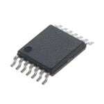
| 描述 | IC OPAMP GP 500KHZ RRO 14TSSOP运算放大器 - 运放 Quad Micropwr Rail-to-Rail |
| 产品分类 | Linear - Amplifiers - Instrumentation, OP Amps, Buffer Amps集成电路 - IC |
| 品牌 | Texas Instruments |
| 产品手册 | http://www.ti.com/litv/slos326f |
| 产品图片 |
|
| rohs | 符合RoHS无铅 / 符合限制有害物质指令(RoHS)规范要求 |
| 产品系列 | 放大器 IC,运算放大器 - 运放,Texas Instruments TLV2764IPWR- |
| 数据手册 | |
| 产品型号 | TLV2764IPWR |
| 产品目录页面 | |
| 产品种类 | 运算放大器 - 运放 |
| 供应商器件封装 | 14-TSSOP |
| 共模抑制比—最小值 | 63 dB |
| 关闭 | No Shutdown |
| 其它名称 | 296-10671-2 |
| 包装 | 带卷 (TR) |
| 单位重量 | 57.200 mg |
| 压摆率 | 0.23 V/µs |
| 商标 | Texas Instruments |
| 增益带宽生成 | 0.5 MHz |
| 增益带宽积 | 500kHz |
| 安装类型 | 表面贴装 |
| 安装风格 | SMD/SMT |
| 封装 | Reel |
| 封装/外壳 | 14-TSSOP(0.173",4.40mm 宽) |
| 封装/箱体 | TSSOP-14 |
| 工作温度 | -40°C ~ 85°C |
| 工作电源电压 | 1.8 V to 3.6 V, +/- 0.8 V to +/- 1.8 V |
| 工厂包装数量 | 2000 |
| 技术 | CMOS |
| 放大器类型 | 通用 |
| 最大双重电源电压 | +/- 1.8 V |
| 最大工作温度 | + 85 C |
| 最小双重电源电压 | +/- 0.8 V |
| 最小工作温度 | - 40 C |
| 标准包装 | 2,000 |
| 电压-电源,单/双 (±) | 1.8 V ~ 3.6 V, ±0.9 V ~ 1.8 V |
| 电压-输入失调 | 550µV |
| 电流-电源 | 20µA |
| 电流-输入偏置 | 3pA |
| 电流-输出/通道 | 10.2mA |
| 电源电流 | 0.112 mA |
| 电路数 | 4 |
| 系列 | TLV2764 |
| 转换速度 | 0.23 V/us |
| 输入偏压电流—最大 | 15 pA |
| 输入参考电压噪声 | 95 nV |
| 输入补偿电压 | 3.5 mV |
| 输出电流 | 10.2 mA |
| 输出类型 | 满摆幅 |
| 通道数量 | 4 Channel |


- 商务部:美国ITC正式对集成电路等产品启动337调查
- 曝三星4nm工艺存在良率问题 高通将骁龙8 Gen1或转产台积电
- 太阳诱电将投资9.5亿元在常州建新厂生产MLCC 预计2023年完工
- 英特尔发布欧洲新工厂建设计划 深化IDM 2.0 战略
- 台积电先进制程称霸业界 有大客户加持明年业绩稳了
- 达到5530亿美元!SIA预计今年全球半导体销售额将创下新高
- 英特尔拟将自动驾驶子公司Mobileye上市 估值或超500亿美元
- 三星加码芯片和SET,合并消费电子和移动部门,撤换高东真等 CEO
- 三星电子宣布重大人事变动 还合并消费电子和移动部门
- 海关总署:前11个月进口集成电路产品价值2.52万亿元 增长14.8%


PDF Datasheet 数据手册内容提取
TLV2760, TLV2761, TLV2762, TLV2763, TLV2764, TLV2765 FAMILY OF 1.8 V MICROPOWER RAIL-TO-RAIL INPUT/OUTPUT OPERATIONAL AMPLIFIERS WITH SHUTDOWN SLOS326F − JUNE 2000 − REVISED AUGUST 2013 (cid:2) Low Supply Voltage...1.8 V to 3.6 V Operational Amplifier (cid:2) Very Low Supply Current...20 μA (per channel) − (cid:2) Ultralow Power Shut-Down Mode + − I = 10 nA/Channel DD(SHDN) (cid:2) CMOS Rail-to-Rail Input/Output (cid:2) Input Common-Mode Voltage SUPPLY CURRENT Range ... −0.2 V to VDD + 0.2 V vs (cid:2) Input Offset Voltage...550 μV SUPPLY VOLTAGE 20 (cid:2) Wide Bandwidth...500 kHz 18 AVVIC= = 1 VDD/2 (cid:2) Slew Rate...0.20 V/μs A 16 TA = 25° C (cid:2) S0°pCe ctoif i7e0d° CTe.m.p.eCroamtumree Rrcaianlg Ge:rade μurrent − 1124 −40°C to 85°C...Industrial Grade y C 10 (cid:2) Ultrasmall Packaging uppl 8 5 or 6 Pin SOT-23 (TLV2760/1) S−D 6 D 4 8 or 10 Pin MSOP (TLV2762/3) I (cid:2) 2 Universal Op-Amp EVM 0 0 0.6 1.2 1.8 2.4 3 3.6 description VDD − Supply Voltage − V The TLV276x single supply operational amplifiers provide 500 kHz bandwidth from only 20 μA while operating down to 1.8 V over the industrial temperature range. The maximum recommended supply voltage is 3.6 V, which allows the devices to be operated from ((cid:2)1.8 V supplies down to (cid:2)0.9 V) two AA or AAA cells. The devices have been characterized at 1.8 V (end of life of 2 AA(A) cells) and at 2.4 V (nominal voltage of 2 NiCd/NiMH cells). The TLV276x have rail-to-rail input and output capability which is a necessity at 1.8 V. The low supply current is coupled with extremely low input bias currents enabling them to be used with mega-ohm resistors. Low shutdown current of only 10 nA make these devices ideal for low frequency measurement applications desiring long active battery life. All members are available in PDIP and SOIC with the singles in the small SOT-23 package, duals in the MSOP, and quads in the TSSOP package. SELECTION OF SINGLE SUPPLY AMPLIFIER PRODUCTS DEVICE V(VDD) (VμIVO) ID(Dμ/AC)h (pIIAB) (GMBHWz) (VS/μRs) (VnnV,1/√kHHzz) (mIOA) DSOHUWTN- RARILA-ITLO- TLV224x 2.5 − 12 600 1 100 0.0055 0.002 NA 0.2 — I/O TLV2211 2.7 − 10 450 13 1 0.065 0.025 21 0.4 — O TLV276x 1.8 − 3.6 550 20 3 0.5 0.23 95 5 Y I/O TLV245x(A) 2.7 − 6 20 23 500 0.22 0.11 49 2.5 Y I/O TLV246x(A) 2.7 − 6 150 550 1300 6.4 1.6 11 25 Y I/O TLV278x(A) 1.8 − 3.6 250 650 2.5 8 5 18 10 Y I/O Please be aware that an important notice concerning availability, standard warranty, and use in critical applications of TexasInstruments semiconductor products and disclaimers thereto appears at the end of this data sheet. PRODUCTION DATA information is current as of publication date. Copyright © 2000−2013, Texas Instruments Incorporated Products conform to specifications per the terms of Texas Instruments standard warranty. Production processing does not necessarily include testing of all parameters. • POST OFFICE BOX 655303 DALLAS, TEXAS 75265 1
TLV2760, TLV2761, TLV2762, TLV2763, TLV2764, TLV2765 FAMILY OF 1.8 V MICROPOWER RAIL-TO-RAIL INPUT/OUTPUT OPERATIONAL AMPLIFIERS WITH SHUTDOWN SLOS326F − JUNE 2000 − REVISED AUGUST 2013 TLV2760 and TLV2761 AVAILABLE OPTIONS(1) PACKAGED DEVICES TTAA AAVTTIO 22m55a°°CCx SSMMAALLLL OOUUTTLLIINNEE SOT-23 PPLLAASSTTIICC DDIIPP (D)† (DBV)‡ SYMBOL (P) TLV2760CD — — — 0°C to 70°C 3500 μV TLV2761CD — — — TLV2760ID TLV2760IDBV VANI TLV2760IP −40°C to 85°C 3500 μV TLV2761ID TLV2761IDBV VAXI TLV2761IP †This package is available taped and reeled. To order this packaging option, add an R suffix to the part number (e.g., TLV2760CDR). ‡This package is only available taped and reeled. For standard quantities (3,000 pieces per reel), add an R suffix (i.e., TLV2760CDBVR). For smaller quantities (250 pieces per mini-reel), add a T suffix to the part number (e.g. TLV2760CDBVT). TLV2762 and TLV2763 AVAILABLE OPTIONS(1) PACKAGED DEVICES TTAA AAVTTIO 22m55a°°CCx OOSUUMTTALLLIINNLEE MSOP PLADDSIIPPTIC PLADDSIIPPTIC (D)† DGK† SYMBOL DGS† SYMBOL (N) (P) TLV2762CD — — — — — — 0°C to 70°C 3500 μV TLV2763CD TLV2762CDGK AJO — — — — TLV2762ID TLV2762IDGK xxTIAJP — — — TLV2762IP −40°C to 85°C 3500 μV TLV2763ID — — TLV2763IDGS xxTIAJR TLV2763IN — †This package is available taped and reeled. To order this packaging option, add an R suffix to the part number (e.g., TLV2762CDR). TLV2764 and TLV2765 AVAILABLE OPTIONS(1) PACKAGED DEVICES TA AVVTIO 2mm5aa°Cx SMALL OUTLINE PLASTIC DIP TSSOP (D)† (N) (PW)† TLV2764CD — — 0°C to 70°C 3500 μV TLV2765CD — — TLV2764ID TLV2764IN TLV2764IPW −40°C to 85°C 3500 μV TLV2765ID TLV2765IN TLV2765IPW †This package is available taped and reeled. To order this packaging option, add an R suffix to the part number (e.g., TLV2764CDR). 1. For the most current package and ordering information, see the Package Option Addendum at the end of this document, or see the TI website at www.ti.com. • 2 POST OFFICE BOX 655303 DALLAS, TEXAS 75265
TLV2760, TLV2761, TLV2762, TLV2763, TLV2764, TLV2765 FAMILY OF 1.8 V MICROPOWER RAIL-TO-RAIL INPUT/OUTPUT OPERATIONAL AMPLIFIERS WITH SHUTDOWN SLOS326F − JUNE 2000 − REVISED AUGUST 2013 TLV276x PACKAGE PINOUTS TLV2760 TLV2760 TLV2761 DBV PACKAGE D OR P PACKAGE DBV PACKAGE (TOP VIEW) (TOP VIEW) (TOP VIEW) OUT 1 6 VDD NC 1 8 SHDN OUT 1 5 VDD IN− 2 7 VDD GND 2 5 SHDN IN+ 3 6 OUT GND 2 GND 4 5 NC IN+ 3 4 IN− IN+ 3 4 IN− TLV2761 TLV2762 TLV2763 D OR P PACKAGE D, DGK, OR P PACKAGE DGS PACKAGE (TOP VIEW) (TOP VIEW) (TOP VIEW) NC 1 8 NC 1OUT 1 8 VDD 1OUT 1 10 VDD IN− 2 7 VDD 1IN− 2 7 2OUT 1IN− 2 9 2OUT IN+ 3 6 OUT 1IN+ 3 6 2IN− 1IN+ 3 8 2IN− GND 4 5 NC GND 4 5 2IN+ GND 4 7 2IN+ 1SHDN 5 6 2SHDN TLV2763 TLV2764 TLV2765 D OR N PACKAGE D, N, OR PW PACKAGE D, N, OR PW PACKAGE (TOP VIEW) (TOP VIEW) (TOP VIEW) 1OUT 1 14 VDD 1OUT 1 14 4OUT 1OUT 1 16 4OUT 1IN− 2 13 2OUT 1IN− 2 13 4IN− 1IN− 2 15 4IN− 1IN+ 3 12 2IN− 1IN+ 3 12 4IN+ 1IN+ 3 14 4IN+ GND 4 11 2IN+ VDD 4 11 GND VDD 4 13 GND NC 5 10 NC 2IN+ 5 10 3IN+ 2IN+ 5 12 3IN+ 1SHDN 6 9 2SHDN 2IN− 6 9 3IN− 2IN− 6 11 3IN− NC 7 8 NC 2OUT 7 8 3OUT 2OUT 7 10 3OUT 1/2SHDN 8 9 3/4SHDN NC − No internal connection • POST OFFICE BOX 655303 DALLAS, TEXAS 75265 3
TLV2760, TLV2761, TLV2762, TLV2763, TLV2764, TLV2765 FAMILY OF 1.8 V MICROPOWER RAIL-TO-RAIL INPUT/OUTPUT OPERATIONAL AMPLIFIERS WITH SHUTDOWN SLOS326F − JUNE 2000 − REVISED AUGUST 2013 absolute maximum ratings over operating free-air temperature range (unless otherwise noted)† Supply voltage, V (see Note 1) . . . . . . . . . . . . . . . . . . . . . . . . . . . . . . . . . . . . . . . . . . . . . . . . . . . . . . . . . . . . . 4 V DD Differential input voltage range, V . . . . . . . . . . . . . . . . . . . . . . . . . . . . . . . . . . . . . . . . . . . . . . . . . . . . . . . . . ±V ID DD Input current range, I . . . . . . . . . . . . . . . . . . . . . . . . . . . . . . . . . . . . . . . . . . . . . . . . . . . . . . . . . . . . . . . . . . . . ±10 mA I Output current range, I . . . . . . . . . . . . . . . . . . . . . . . . . . . . . . . . . . . . . . . . . . . . . . . . . . . . . . . . . . . . . . . . . ±10 mA O Continuous total power dissipation . . . . . . . . . . . . . . . . . . . . . . . . . . . . . . . . . . . . . See Dissipation Rating Table Operating free-air temperature range, T : C-suffix . . . . . . . . . . . . . . . . . . . . . . . . . . . . . . . . . . . . . . 0°C to 70°C A I-suffix . . . . . . . . . . . . . . . . . . . . . . . . . . . . . . . . . . . . −40°C to 85°C Maximum junction temperature, T . . . . . . . . . . . . . . . . . . . . . . . . . . . . . . . . . . . . . . . . . . . . . . . . . . . . . . . . . 150°C J Storage temperature range, T . . . . . . . . . . . . . . . . . . . . . . . . . . . . . . . . . . . . . . . . . . . . . . . . . . . −65°C to 150°C stg Lead temperature 1,6 mm (1/16 inch) from case for 10 seconds . . . . . . . . . . . . . . . . . . . . . . . . . . . . . . . 260°C †Stresses beyond those listed under “absolute maximum ratings” may cause permanent damage to the device. These are stress ratings only, and functional operation of the device at these or any other conditions beyond those indicated under “recommended operating conditions” is not implied. Exposure to absolute-maximum-rated conditions for extended periods may affect device reliability. NOTE 1: All voltage values, except differential voltages, are with respect to GND DISSIPATION RATING TABLE PPAACCKKAAGGEE ΘΘJJCC ΘΘJJAA TTAA ≤≤ 2255°CC TTAA == 8855°CC (°C/W) (°C/W) POWER RATING POWER RATING D (8) 38.3 176 710 mW 369 mW D (14) 26.9 122 1022 mW 531 mW D (16) 25.7 114 1090 mW 567 mW DBV (5) 55 324 385 mW 201 mW DBV (6) 55 294 425 mW 221 mW DGK(8) 54.2 260 481 mW 250 mW DGS(10) 54.1 258 485 mW 252 mW N (14,16) 32 78 1600 mW 833 mW P 41 104 1200 mW 625 mW PW (14) 29.3 174 720 mW 374 mW PW (16) 28.7 161 774 mW 403 mW recommended operating conditions MIN MAX UNIT Single supply 1.8 3.6 SSuuppppllyy vvoollttaaggee, VVDD Split supply ±0.8 ±1.8 VV Common-mode input voltage range, VICR −0.2 VDD+0.2 V C-suffix 0 70 OOppeerraattiinngg ffrreeee-aaiirr tteemmppeerraattuurree, TTA °°CC I-suffix −40 85 VDD < 2.7 V 0.75 VDD VVIH Shutdown on//off voltagge level ((see Note 2)) VDD = 2.7 to 3.6 V 2 V VIL 0.6 NOTE 2: Relative to GND • 4 POST OFFICE BOX 655303 DALLAS, TEXAS 75265
TLV2760, TLV2761, TLV2762, TLV2763, TLV2764, TLV2765 FAMILY OF 1.8 V MICROPOWER RAIL-TO-RAIL INPUT/OUTPUT OPERATIONAL AMPLIFIERS WITH SHUTDOWN SLOS326F − JUNE 2000 − REVISED AUGUST 2013 electrical characteristics at recommended operating conditions, V = 1.8 V, 2.4 V (unless DD otherwise noted) dc performance PARAMETER TEST CONDITIONS TA† MIN TYP MAX UNIT VIC = VDD/2, 25°C 550 3500 VVIO IInnppuutt ooffffsseett vvoollttaaggee VVO = VVDD//22, TTLLVV227766xx Full range 6800 μVV RRLL == 330000 kkΩΩ, αVIO Offset voltage drift RS = 50 Ω 9 μV/°C 25°C 50 70 VVDD = 11.88 VV ddBB Full range 48 VVRIISCC RR= ==5 000 ΩVV ttoo VVDDDD,, VVDD = 22.44 VV Fu2ll 5r°aCnge 5530 72 ddBB CCMMRRRR CCoommmmoonn-mmooddee rreejjeeccttiioonn rraattiioo 25°C 55 76 VVDD = 33.66 VV ddBB Full range 55 RVVIISCC RR= ==5 011..Ω22 VV ttoo VVDDDD,, VVDD = 22.44 VV, 33.66 VV Fu2ll 5r°aCnge 6630 82 ddBB 25°C 20 60 VVDD = 11.88 VV Full range 18 VV//mmVV AAVD LLaaamrrpggleeif-issciiaggtnnioaanll ddiiffffeerreennttiiaall vvoollttaaggee RRVOOLL ((==P P11))00 = kk VΩΩD,,D/2 VVDD = 22.44 VV Fu2ll 5r°aCnge 2283 78 25°C 45 120 VVDD = 33.66 VV Full range 37 VV//mmVV †Full range is 0°C to 70°C for the C-suffix and −40°C to 85°C for the I-suffix. If not specified, full range is −40°C to 85°C. input characteristics PARAMETER TEST CONDITIONS TA† MIN TYP MAX UNIT 25°C 3 15 IIIIOO IInnppuutt ooffffsseett ccuurrrreenntt VVIICC == VVDDDD//22,, TLV276xC Full range 100 ppAA VVOO == VVDDDD//22,, TLV276xI Full range 200 RLL = 300 kΩ, 25°C 3 15 IIIIBB IInnppuutt bbiiaass ccuurrrreenntt RS = 50 Ω TLV276xC Full range 100 ppAA TLV276xI Full range 200 ri(d) Differential input resistance 25°C 1000 GΩ ci(c) Common-mode input capacitance f = 16 kHz 25°C 10 pF †Full range is 0°C to 70°C for the C-suffix and −40°C to 85°C for the I-suffix. If not specified, full range is −40°C to 85°C. • POST OFFICE BOX 655303 DALLAS, TEXAS 75265 5
TLV2760, TLV2761, TLV2762, TLV2763, TLV2764, TLV2765 FAMILY OF 1.8 V MICROPOWER RAIL-TO-RAIL INPUT/OUTPUT OPERATIONAL AMPLIFIERS WITH SHUTDOWN SLOS326F − JUNE 2000 − REVISED AUGUST 2013 electrical characteristics at recommended operating conditions, V = 1.8 V, 2.4 V (unless DD otherwise noted) (continued) output characteristics PARAMETER TEST CONDITIONS TA† MIN TYP MAX UNIT 25°C 1.77 1.79 VVDD = 11.88VV Full range 1.76 VVIOOIICCH === −VVDD10DD0//22 μ,,A VVDD = 22.44VV Fu2ll 5r°aCnge 22..3387 2.39 25°C 3.58 3.59 VVDD = 33.66VV Full range 3.57 VVOH HHiigghh-lleevveell oouuttppuutt vvoollttaaggee 25°C 1.725 1.75 VV VVDD = 11.88VV Full range 1.7 VVIOOIICCH === −VVDD50DD0//22 μ,,A VVDD = 22.44VV Fu2ll 5r°aCnge 2.322.53 2.35 25°C 3.525 3.55 VVDD = 33.66VV Full range 3.5 25°C 10 20 VVIC = VVDD//22, IIOL = 110000 μAA Full range 30 VVOL LLooww-lleevveell oouuttppuutt vvoollttaaggee 25°C 50 75 mmVV VVIC = VVDD//22, IIOL = 550000 μAA Full range 100 VVDDDD == 11..88 VV,, Positive rail 2255°°CC 4.8 VO = 0.5 V from Negative rail 7.2 IIO OOuuttppuutt ccuurrrreenntt VVDDDD == 22..44 VV,, Positive rail 2255°°CC 7.3 mmAA VO = 0.5 V from Negative rail 10.2 Sourcing 7 VVDD = 11.88 VV Sinking 2255°°CC 10 IIOS SShhoorrtt-cciirrccuuiitt oouuttppuutt ccuurrrreenntt Sourcing 15 mmAA VVDD = 22.44 VV Sinking 2255°°CC 19 †Full range is 0°C to 70°C for the C-suffix and −40°C to 85°C for the I-suffix. If not specified, full range is −40°C to 85°C. power supply, V = 1.8 V, 2.4 V, 3.6 V (unless otherwise noted) DD PARAMETER TEST CONDITIONS TA† MIN TYP MAX UNIT 25°C 20 28 IIDD SSuuppppllyy ccuurrrreenntt ((ppeerr cchhaannnneell)) VVO = VVDD//22, SHDN = VDD Full range 30 μAA VVDDDD == 11..88 VV ttoo 22..44 VV,, 25°C 65 85 VIC = VDD/2 Full range 63 kkSVR SS(ΔuuVppDppDllyy /vvΔooVllttIaaOOgg)ee rreejjeeccttiioonn rraattiioo VVVDDICDD = == V 22D..44D /VV2 ttoo 33..66 VV,, NNoo llooaadd Fu2ll 5r°aCnge 6653 85 ddBB VVDDDD == 11..88 VV ttoo 33..66 VV,, 25°C 65 85 VIC = VDD/2 Full range 63 †Full range is 0°C to 70°C for the C-suffix and −40°C to 85°C for the I-suffix. If not specified, full range is −40°C to 85°C. • 6 POST OFFICE BOX 655303 DALLAS, TEXAS 75265
TLV2760, TLV2761, TLV2762, TLV2763, TLV2764, TLV2765 FAMILY OF 1.8 V MICROPOWER RAIL-TO-RAIL INPUT/OUTPUT OPERATIONAL AMPLIFIERS WITH SHUTDOWN SLOS326F − JUNE 2000 − REVISED AUGUST 2013 electrical characteristics at recommended operating conditions, V = 1.8 V, 2.4 V (unless DD otherwise noted) (continued) dynamic performance PARAMETER TEST CONDITIONS TA† MIN TYP MAX UNIT UGBW Unity gain bandwidth RL = 300 kΩ, CL = 10 pF 25°C 500 kHz 25°C 0.11 0.20 VVDD = 11.88 VV Full range 0.09 VV//μss SSRR+ PPunooisstyiitt iigvvaeei nsslleeww rraattee aatt VVCOOL ((=PP PP5))0 == p 11F ,VV,, RRLL == 330000 kkΩΩ,, VVDD = 22.44 VV Fu2ll 5r°aCnge 00..0119 0.22 25°C 0.11 0.23 VVDD = 33.66 VV Full range 0.09 VV//μss 25°C 0.08 0.15 VVDD = 11.88 VV Full range 0.07 VV//μss SSRR− NNuneeiggtyaa gttiivvaeein sslleeww rraattee aatt VVCOOL ((=PP PP5))0 == p 11F ,VV,, RRLL == 330000 kkΩΩ,, VVDD = 22.44 VV Fu2ll 5r°aCnge 00..1009 0.18 25°C 0.10 0.22 VVDD = 33.66 VV Full range 0.09 VV//μss φm PGhaains em maragrignin RRL = 330000 kkΩΩ, CCL = 110000 ppFF 2255°°CC 6230 d°B VVDDDD == 11..88 VV,, VV((SSTTEEPP))PPPP == 11 VV,, 0.1% 6.4 AV = −1, CL = 10 pF, RL = 300 kΩ 0.01% 13.7 tts SSeettttlliinngg ttiimmee VVDDDD == 22..44 VV,, VV((SSTTEEPP))PPPP == 11 VV,, 0.1% 2255°°CC 6 μss AV = −1, CL = 10 pF, RL = 300 kΩ 0.01% 13.9 †Full range is 0°C to 70°C for the C-suffix and −40°C to 85°C for the I-suffix. If not specified, full range is −40°C to 85°C. noise/distortion PARAMETER TEST CONDITIONS TA MIN TYP MAX UNIT VDDDD = 1.8 V,, AV = 1 0.08% VRROLL (==P P33)00 =00 VkkΩΩDD,/2 V, AV = 10 25°C 0.10% f = 1 kHz AV = 100 0.27% TTHHDD + NN TToottaall hhaarrmmoonniicc ddiissttoorrttiioonn pplluuss nnooiissee VDDDD = 2.4 V,, AV = 1 0.06% VRROLL (==P P33)00 =00 VkkΩΩDD,/2 V, AV = 10 25°C 0.08% f = 1 kHz AV = 100 0.24% f = 1 kHz 25°C 95 VVn EEqquuiivvaalleenntt iinnppuutt nnooiissee vvoollttaaggee f = 10 kHz 25°C 75 nnVV//√√HHzz In Equivalent input noise current f = 1 kHz 25°C 0.8 fA/√Hz shutdown characteristics PARAMETER TEST CONDITIONS TA† MIN TYP MAX UNIT SSuuppppllyy ccuurrrreenntt,, aallll cchhaannnneellss iinn sshhuuttddoowwnn mmooddee 25°C 10 50 IIDD(SHDN) (TLV2760, TLV2763, TLV2765) (per channel) SSHHDDNN = 00 VV Full range 400 nnAA t(on) Amplifier turnon time (see Note 3) RL = 300 kΩ 25°C 5 μs t(off) Amplifier turnoff time (see Note 3) RL = 300 kΩ 25°C 0.8 μs †Full range is 0°C to 70°C for the C-suffix and −40°C to 85°C for the I-suffix. If not specified, full range is −40°C to 85°C. NOTE 3: Disable time and enable time are defined as the interval between application of the logic signal to SHDN and the point at which the supply current has reached half its final value. • POST OFFICE BOX 655303 DALLAS, TEXAS 75265 7
TLV2760, TLV2761, TLV2762, TLV2763, TLV2764, TLV2765 FAMILY OF 1.8 V MICROPOWER RAIL-TO-RAIL INPUT/OUTPUT OPERATIONAL AMPLIFIERS WITH SHUTDOWN SLOS326F − JUNE 2000 − REVISED AUGUST 2013 TYPICAL CHARACTERISTICS Table of Graphs FIGURE VIO Input offset voltage vs Common-mode input voltage 1, 2 CMRR Common-mode rejection ratio vs Frequency 3 VOH High-level output voltage vs High-level output current 4, 6 VOL Low-level output voltage vs Low-level output current 5, 7 VO(PP) Maximum peak-to-peak output voltage vs Frequency 8 IDD Supply current vs Supply voltage 9 IDD Supply current vs Free-air temperature 10 PSRR Power supply rejection ratio vs Frequency 11 AVD Differential voltage amplification & phase vs Frequency 12 vs Temperature 13 GGaaiinn-bbaannddwwiiddtthh pprroodduucctt vs Supply voltage 14 vs Supply voltage 15 SSRR SSlleeww rraattee vs Free-air temperature 16, 17 φm Phase margin vs Load capacitance 18 Vn Equivalent input noise voltage vs Frequency 19 Supply current and output voltage vs Time 20 Voltage-follower large-signal pulse response vs Time 21 Voltage-follower small-signal pulse response vs Time 22 Inverting large-signal response vs Time 23 Inverting small-signal response vs Time 24 Crosstalk vs Frequency 25 Shutdown forward & reverse isolation vs Frequency 26 IDD(SHDN) Shutdown supply current vs Supply voltage 27 IDD(SHDN) Shutdown supply current vs Free-air temperature 28 IDD(SHDN) Shutdown pin leakage current vs Shutdown pin voltage 29 IDD(SHDN) Shutdown supply current/output voltage vs Time 30 • 8 POST OFFICE BOX 655303 DALLAS, TEXAS 75265
TLV2760, TLV2761, TLV2762, TLV2763, TLV2764, TLV2765 FAMILY OF 1.8 V MICROPOWER RAIL-TO-RAIL INPUT/OUTPUT OPERATIONAL AMPLIFIERS WITH SHUTDOWN SLOS326F − JUNE 2000 − REVISED AUGUST 2013 TYPICAL CHARACTERISTICS INPUT OFFSET VOLTAGE INPUT OFFSET VOLTAGE COMMON-MODE REJECTION RATIO vs vs vs COMMON-MODE INPUT VOLTAGE COMMON-MODE INPUT VOLTAGE FREQUENCY 300 350 B140 VDD=1.8 V VDD=2.4 V − d130 μoltage −V 122505000 TA=25° C μVoltage −V 223050000 TA=25 °C Rejection Ratio 1110128900000 VDD = 2.4 V Input Offset V− 105000 Input Offset −O 11055000 Common-Mode 3456700000 VDD = 1.8 V VIO −50 VI 0 R − 20 R 10 −100 −50 CM 0 −0.2 0 0.2 0.40.60.8 1 1.2 1.4 1.6 1.8 2 −0.2 0.2 0.6 1 1.4 1.8 2.2 2.6 1 10 100 1k 10k 100k 1M VICR − Common-Mode Input Voltage − V VICR − Common-Mode Input Voltage − V f − Frequency − Hz Figure 1 Figure 2 Figure 3 HIGH-LEVEL OUTPUT VOLTAGE LOW-LEVEL OUTPUT VOLTAGE HIGH-LEVEL OUTPUT VOLTAGE vs vs vs HIGH-LEVEL OUTPUT CURRENT LOW-LEVEL OUTPUT CURRENT HIGH-LEVEL OUTPUT CURRENT 1.8 1.8 2.4 − High-Level Output Voltage − VH 00001111........24680246 TTTTTAAAAA=====−28704550°0°C°°°CCCC VDD=1.8 V − Low-Level Output Voltage − VL 00001111........24680246 VDD=T1AT.A=T8=A−TT V=24AA500==°°°87CCC50°°CC − High-Level Output Voltage − VH 0001112.......3692581 TTTATAAA=T===A−87=2450500°°°°°CCCCC VDD = 2.4 V O O O V 0.0 V 0.0 V 0 0 1 2 3 4 5 6 7 8 0 1 2 3 4 5 6 7 8 9 10 11 12 0 2 4 6 8 10 12 14 16 18 20 IOH − High-Level Output Current − mA IOL − Low-Level Output Current − mA IOH − High-Level Output Current − mA Figure 4 Figure 5 Figure 6 MAXIMUM PEAK-TO-PEAK LOW-LEVEL OUTPUT VOLTAGE OUTPUT VOLTAGE vs vs LOW-LEVEL OUTPUT CURRENT − V FREQUENCY 2.4 ge 2.8 el Output Voltage − V 1112....2581 VDDTTT=ATAA A=T2===A−. 48=247 55000V°°°°°CCCCC k-To-Peak Output Volta 1112222.......4680246 VOV(OP(PP)P=) =1 .28. 4V V v a Le 0.9 Pe 1.2 ow- um 1.0 V− LOL 000...036 − MaximPP) 0000....4682 ARTCAVLL = ===3 210−5001° 0pk CΩF 0 2.5 5 7.5 10 12.5 1517.5 20 22.525 O( 10 100 1k 10k 100k 1M IOL − Low-Level Output Current − mA V f − Frequency − Hz Figure 7 Figure 8 • POST OFFICE BOX 655303 DALLAS, TEXAS 75265 9
TLV2760, TLV2761, TLV2762, TLV2763, TLV2764, TLV2765 FAMILY OF 1.8 V MICROPOWER RAIL-TO-RAIL INPUT/OUTPUT OPERATIONAL AMPLIFIERS WITH SHUTDOWN SLOS326F − JUNE 2000 − REVISED AUGUST 2013 TYPICAL CHARACTERISTICS SUPPLY CURRENT SUPPLY CURRENT POWER SUPPLY REJECTION RATIO vs vs vs SUPPLY VOLTAGE FREE-AIR TEMPERATURE FREQUENCY 20 24 B 100 μISupply Current − −ADD 1111102486468 TAVAVI C== = 81 5V°DCD/2 TATT ATA= A = =7 = 0−0 °42°C0C5°°CC I− Supply Current − mADD 111122246802 VDD = 2.4 V VVDDDD = = 1 3.8.6 V V − Power Supply Rejection Ratio − d 246800000 VTAD=D2=52°.C4 V 2 RR S 0 10 P −20 0 0.6 1.2 1.8 2.4 3 3.6 −40 −15 10 35 60 85 10 100 1k 10k 100k 1M VDD − Supply Voltage − V TA − Free-Air Temperature − °C f − Frequency − Hz Figure 9 Figure 10 Figure 11 DIFFERENTIAL VOLTAGE GAIN AND PHASE GAIN BANDWIDTH PRODUCT vs vs FREQUENCY TEMPERATURE 100 180 700 ge Gain − dB 8600 Phase 1196520000 °n − Product − kHz 560000 VDD = 2.4 V RCf =LL 1==0 13 k00H 0p zFkΩ ntial Volta 2400 30−030 ase Margi andwidth 340000 VDD = 1.8 V e h B er Gain −60 P n − Diff 0 VRDL=D 3=0 10. 8k ΩV & 2.4 V −90 − Gai 200 AVD −20 CTAL == 2150° p CF −−112500 BWP 100 G −40 −180 0 10 100 1k 10k 100k 1M −40 −25 −10 5 20 35 50 65 80 85 f − Frequency − Hz TA − Temperature − °C Figure 12 Figure 13 GAIN-BANDWIDTH PRODUCT SLEW RATE vs vs SUPPLY VOLTAGE SUPPLY VOLTAGE 560 0.36 Hz RL = 300 kΩ − k 540 CL = 10 pF 0.32 ct f = 10 kHz odu 520 Ta = 25°C μs 0.28 SR+ P − Gain Bandwidth Pr 444546800000 SR − Slew Rate − V/ 00000.....0112282604 SR− ARCTAVLL ==== 5213050 °0p FCkΩ W B 420 0.04 G 400 0.00 11.21.41.61.8 2 2.22.42.62.8 3 3.23.43.6 1.8 2 2.2 2.4 2.6 2.8 3 3.2 3.4 3.6 VDD − Supply Voltage − V VDD − Supply Voltage − V Figure 14 Figure 15 • 10 POST OFFICE BOX 655303 DALLAS, TEXAS 75265
TLV2760, TLV2761, TLV2762, TLV2763, TLV2764, TLV2765 FAMILY OF 1.8 V MICROPOWER RAIL-TO-RAIL INPUT/OUTPUT OPERATIONAL AMPLIFIERS WITH SHUTDOWN SLOS326F − JUNE 2000 − REVISED AUGUST 2013 TYPICAL CHARACTERISTICS SLEW RATE SLEW RATE PHASE MARGIN vs vs vs FREE-AIR TEMPERATURE FREE-AIR TEMPERATURE LOAD CAPACITANCE 0.32 0.32 90 0.28 0.28 SR+ 80 Rnull=0 Ω μSR − Slew Rate − V/s 000000......001122482604 SSRR+− VARCVVDILLC ==D= 35= =100 V 0 1pD .kF8DΩ /V2 μSR − Slew Rate − V/s 000000......011220826044 SR− AVRCVDVILLC= D== = 3=51 0V 020D .p 4DkF Ω/V2 φ°− Phase Margin − m 12345670000000 VRATADVL D=== =23O 502p°0.eC4 kn VΩ L oop Rnull=100 Ω 0.00 0.00 0 −40 −25 −10 5 20 35 50 65 8085 −40 −15 10 35 60 85 10 100 1k TA − Free-Air Temperature − °C TA − Free-Air Temperature − °C CL − Load Capacitance − pF Figure 16 Figure 17 Figure 18 SUPPLY CURRENT AND OUTPUT VOLTAGE EQUIVALENT INPUT NOISE VOLTAGE vs vs TIME FREQUENCY 20 Hz 500 nV/quivalent Input Noise Voltage − 12233441505050505000000000 VDD = 1.8V VDD = 2.4 V TA = 25°C μ− Supply Current −IADD 110505 IDVDO VAVRCTAVDILLN D==== = 2131 =V500 3D°0 pC.D 6kF/ Ω2V 00112..55 − Output Voltage − VVO E −0.5 − 0 0 1 2 3 4 5 n 10 100 1k 10k 100k V f − Frequency − Hz t − Time − μs Figure 19 Figure 20 VOLTAGE-FOLLOWER LARGE-SIGNAL PULSE RESPONSE VOLTAGE-FOLLOWER SMALL-SIGNAL PULSE RESPONSE vs vs TIME TIME − Input Voltage − VVI 102...102555 0 0.2VARCTAVDLL0 D====.4 1 231=5000 2°0 .pC6. 4kF ΩV0.8 1 1.2VVI1O.4 1.6 1.8011220...555 − Output Voltage − VVO − Input Voltage − VVI1111111.......11122224680246 0 1 CTVARAVDLL2 D==== 2131=500 32°0 pC. 4kF ΩV4 5 VV6OI 7 81111111.......12222118024646 − Output Voltage − VVO t − Time − μs t − Time − μs Figure 21 Figure 22 • POST OFFICE BOX 655303 DALLAS, TEXAS 75265 11
TLV2760, TLV2761, TLV2762, TLV2763, TLV2764, TLV2765 FAMILY OF 1.8 V MICROPOWER RAIL-TO-RAIL INPUT/OUTPUT OPERATIONAL AMPLIFIERS WITH SHUTDOWN SLOS326F − JUNE 2000 − REVISED AUGUST 2013 TYPICAL CHARACTERISTICS INVERTING LARGE-SIGNAL RESPONSE INVERTING SMALL-SIGNAL PULSE RESPONSE vs vs TIME TIME − Input Voltage − VVI 012...012555 VRCTAAVDLL D==== 2131=500 2°0 pC. 4kF ΩV VVIO 01122...555 − Output Voltage − V − Input Voltage − VVI11111.....1122226048 VVIVRCATOAVDLL D==== 2131=500 2°0 pC. 4kF ΩV 1111....12226048 − Output Voltage − V 0 10 20 30 40 50 60 70 80 900 VO 0 5 10 15 20 25 30 35 40 451.12 VO t − Time − μs t − Time − μs Figure 23 Figure 24 SHUTDOWN FORWARD AND CROSSTALK REVERSE ISOLATION vs vs FREQUENCY FREQUENCY B 0 d 100 Crosstalk − dB −−−−−10864200000 CVVART ArADIVLo l =l= Ds ==C s V 3=21th0a D5a10lDk°.n 8C/ kn2i nΩVe lS s&h u2t.d4o Vwn n Forward and Reverse Isolation − 2345678900000000 CVVRDILL = =D= V 1=30D 01 D0p.8 FF/k 2o&Ωr w2.a4r dV and Reverse Isolation −120 Crosstalk/No Shutdown utdow 10 ATAV = = 2+51°C −140 h 0 10 100 1k 10k 100k S 10 100 1k 10k 100k 1M f − Frequency − Hz f − Frequency − Hz Figure 25 Figure 26 SHUTDOWN SUPPLY CURRENT SHUTDOWN SUPPLY CURRENT SHUTDOWN PIN LEAKAGE CURRENT vs vs vs SUPPLY VOLTAGE FREE-AIR TEMPERATURE SHUTDOWN PIN VOLTAGE .014 .12 A 20 p μCurrent − A ..001102 SVAVHIN D= = N1 V =D D0/ 2V TA = 25°C μCurrent −A ..0180 VSVA VHDIN DD == N= 1V 1=D. 8D0,/V 22.4, 3.6 V ge Current − 1105 VTAD D= =8 53°.C6 V Supply .008 Supply .06 n Leaka 5 − Shutdown DD ...000000246 TA = 0T°AC = −40°C Shutdown −DD ..0024 Shutdown Pi−D −−1005 I I D 0 0 I −15 0 0.4 0.8 1.2 1.6 2 2.4 2.8 3.2 3.6 −40 −25 −10 5 20 35 50 65 80 85 0 0.4 0.8 1.2 1.6 2 2.4 2.8 3.2 3.6 VDD − Supply Voltage − V TA − Free-Air Temperature − °C Shutdown Pin Voltage − V Figure 27 Figure 28 Figure 29 • 12 POST OFFICE BOX 655303 DALLAS, TEXAS 75265
TLV2760, TLV2761, TLV2762, TLV2763, TLV2764, TLV2765 FAMILY OF 1.8 V MICROPOWER RAIL-TO-RAIL INPUT/OUTPUT OPERATIONAL AMPLIFIERS WITH SHUTDOWN SLOS326F − JUNE 2000 − REVISED AUGUST 2013 TYPICAL CHARACTERISTICS SHUTDOWN SUPPLY CURRENT / OUTPUT VOLTAGE vs TIME − V 3.0 se 2.5 ul P 2.0 n ow 1.5 d ut 1.0 SHDN h − S 0.5 DN 0.0 H S −0.5 1.5 − V 1.3 oltage 01..80 VO V put 0.5 ut O 0.3 − O 0.0 V −0.3 VDD = 2.4 V AV = 1 μnt − A 111648 RCLL == 31000 p kFΩ Curre 1102 VTAIC = = 2 V5D°DC/2 y pl 8 p − Su 46 IDD(SHDN = 0) D D 2 I 0 −2 20 40 60 80 100 120 140 160 t − Time − μs Figure 30 • POST OFFICE BOX 655303 DALLAS, TEXAS 75265 13
TLV2760, TLV2761, TLV2762, TLV2763, TLV2764, TLV2765 FAMILY OF 1.8 V MICROPOWER RAIL-TO-RAIL INPUT/OUTPUT OPERATIONAL AMPLIFIERS WITH SHUTDOWN SLOS326F − JUNE 2000 − REVISED AUGUST 2013 APPLICATION INFORMATION driving a capacitive load When the amplifier is configured in this manner, capacitive loading directly on the output will decrease the device’s phase margin leading to high frequency ringing or oscillations. Therefore, for capacitive loads of greater than 10 pF, it is recommended that a resistor be placed in series (R ) with the output of the amplifier, as NULL shown in Figure 31. A minimum value of 20 Ω should work well for most applications. RF RG Input − RNULL Output + CLOAD VDD/2 Figure 31. Driving a Capacitive Load offset voltage The output offset voltage, (V ) is the sum of the input offset voltage (V ) and both input bias currents (I ) times OO IO IB the corresponding gains. The following schematic and formula can be used to calculate the output offset voltage: RF IIB− RG + − VI VO + RS (cid:4) IIB+(cid:6) (cid:4) (cid:6) (cid:4) (cid:6) (cid:4) (cid:6) R R VOO(cid:3)VIO 1(cid:5) RF (cid:2)IIB(cid:5)RS 1(cid:5) RF (cid:2)IIB–RF G G Figure 32. Output Offset Voltage Model general configurations When receiving low-level signals, limiting the bandwidth of the incoming signals into the system is often required. The simplest way to accomplish this is to place an RC filter at the noninverting terminal of the amplifier (see Figure 33). • 14 POST OFFICE BOX 655303 DALLAS, TEXAS 75265
TLV2760, TLV2761, TLV2762, TLV2763, TLV2764, TLV2765 FAMILY OF 1.8 V MICROPOWER RAIL-TO-RAIL INPUT/OUTPUT OPERATIONAL AMPLIFIERS WITH SHUTDOWN SLOS326F − JUNE 2000 − REVISED AUGUST 2013 APPLICATION INFORMATION general configurations (continued) RG RF VDD/2 − + VO VI R1 C1 f (cid:3) 1 –3dB 2(cid:2)R1C1 (cid:4) (cid:6) V R (cid:4) (cid:6) O (cid:3) 1(cid:5) F 1 V R 1(cid:5)2(cid:2)fR1C1 I G Figure 33. Single-Pole Low-Pass Filter If even more attenuation is needed, a multiple pole filter is required. The Sallen-Key filter can be used for this task. For best results, the amplifier should have a bandwidth that is 8 to 10 times the filter frequency bandwidth. Failure to do this can result in phase shift of the amplifier. C1 R1 = R2 = R C1 = C2 = C Q = Peaking Factor (Butterworth Q = 0.707) VI + R1 R2 _ f (cid:3) 1 –3dB 2(cid:2)RC C2 RG = RF RF (2 − 1 ) RG Q VDD/2 Figure 34. 2-Pole Low-Pass Sallen-Key Filter circuit layout considerations To achieve the levels of high performance of the TLV276x, follow proper printed-circuit board design techniques. A general set of guidelines is given in the following. (cid:2) Ground planes—It is highly recommended that a ground plane be used on the board to provide all components with a low inductive ground connection. However, in the areas of the amplifier inputs and output, the ground plane can be removed to minimize the stray capacitance. (cid:2) Proper power supply decoupling—Use a 6.8-μF tantalum capacitor in parallel with a 0.1-μF ceramic capacitor on each supply terminal. It may be possible to share the tantalum among several amplifiers depending on the application, but a 0.1-μF ceramic capacitor should always be used on the supply terminal of every amplifier. In addition, the 0.1-μF capacitor should be placed as close as possible to the supply terminal. As this distance increases, the inductance in the connecting trace makes the capacitor less effective. The designer should strive for distances of less than 0.1 inches between the device power terminals and the ceramic capacitors. • POST OFFICE BOX 655303 DALLAS, TEXAS 75265 15
TLV2760, TLV2761, TLV2762, TLV2763, TLV2764, TLV2765 FAMILY OF 1.8 V MICROPOWER RAIL-TO-RAIL INPUT/OUTPUT OPERATIONAL AMPLIFIERS WITH SHUTDOWN SLOS326F − JUNE 2000 − REVISED AUGUST 2013 APPLICATION INFORMATION circuit layout considerations (continued) (cid:2) Sockets—Sockets can be used but are not recommended. The additional lead inductance in the socket pins will often lead to stability problems. Surface-mount packages soldered directly to the printed-circuit board is the best implementation. (cid:2) Short trace runs/compact part placements—Optimum high performance is achieved when stray series inductance has been minimized. To realize this, the circuit layout should be made as compact as possible, thereby minimizing the length of all trace runs. Particular attention should be paid to the inverting input of the amplifier. Its length should be kept as short as possible. This will help to minimize stray capacitance at the input of the amplifier. (cid:2) Surface-mount passive components—Using surface-mount passive components is recommended for high performance amplifier circuits for several reasons. First, because of the extremely low lead inductance of surface-mount components, the problem with stray series inductance is greatly reduced. Second, the small size of surface-mount components naturally leads to a more compact layout thereby minimizing both stray inductance and capacitance. If leaded components are used, it is recommended that the lead lengths be kept as short as possible. shutdown function Three members of the TLV276x family (TLV2760/3/5) have a shutdown terminal for conserving battery life in portable applications. When the shutdown terminal is pulled low, the supply current is reduced to 10 nA/channel, the amplifier is disabled, and the outputs are placed in a high impedance mode. To enable the amplifier, the shutdown terminal must be pulled high. The shutdown terminal should never be left floating. If the shutdown feature is not desired, directly tie the shutdown terminal to the positive rail. The shutdown terminal threshold is always referenced to the GND terminal of the device. Therefore, when operating the device with split supply voltages (e.g. ±1.8 V), the shutdown terminal needs to be pulled to the negative rail, not the system ground, to disable the operational amplifier. The amplifier is powered with a single 2.4-V supply and configured as a noninverting configuration with a unity gain. Turnon and turnoff times are defined as the interval between application of the logic signal to the shutdown pin and the point at which the supply current has reached half its final value. The times for the single, dual, and quad are listed in the data tables. general power dissipation considerations For a given θ , the maximum power dissipation is shown in Figure 35 and is calculated by the following formula: JA (cid:4) (cid:6) T (cid:7)T P (cid:3) MAX A D (cid:2) JA Where: P = Maximum power dissipation of TLV276x IC (watts) D T = Absolute maximum junction temperature (150°C) MAX T = Free-ambient air temperature (°C) A θJA = θJC + θCA θ = Thermal coefficient from junction to case JC θ = Thermal coefficient from case to ambient air (°C/W) CA • 16 POST OFFICE BOX 655303 DALLAS, TEXAS 75265
TLV2760, TLV2761, TLV2762, TLV2763, TLV2764, TLV2765 FAMILY OF 1.8 V MICROPOWER RAIL-TO-RAIL INPUT/OUTPUT OPERATIONAL AMPLIFIERS WITH SHUTDOWN SLOS326F − JUNE 2000 − REVISED AUGUST 2013 APPLICATION INFORMATION general power dissipation considerations (continued) MAXIMUM POWER DISSIPATION vs FREE-AIR TEMPERATURE 2 PDIP Package TJ = 150°C 1.75 Low-K Test PCB θJA = 104°C/W W n − 1.5 MSOP Package o pati 1.25 SOIC Package LθJoAw =-K 2 6T0e°sCt /PWCB si Low-K Test PCB Dis θJA = 176°C/W r 1 e w o P m 0.75 u m xi 0.5 a M 0.25 SOT-23 Package Low-K Test PCB 0 θJA = 324°C/W −55−40−25 −10 5 20 35 50 65 80 95 110 125 TA − Free-Air Temperature − °C NOTE A: Results are with no air flow and using JEDEC Standard Low-K test PCB. Figure 35. Maximum Power Dissipation vs Free-Air Temperature • POST OFFICE BOX 655303 DALLAS, TEXAS 75265 17
TLV2760, TLV2761, TLV2762, TLV2763, TLV2764, TLV2765 FAMILY OF 1.8 V MICROPOWER RAIL-TO-RAIL INPUT/OUTPUT OPERATIONAL AMPLIFIERS WITH SHUTDOWN SLOS326F − JUNE 2000 − REVISED AUGUST 2013 APPLICATION INFORMATION macromodel information Macromodel information provided was derived using Microsim Parts™ Release 9.1, the model generation software used with Microsim PSpice™. The Boyle macromodel (see Note 4) and subcircuit in Figure 36 are generated using TLV276x typical electrical and operating characteristics at T = 25°C. Using this information, A output simulations of the following key parameters can be generated to a tolerance of 20% (in most cases): (cid:2) (cid:2) Maximum positive output voltage swing Unity-gain frequency (cid:2) (cid:2) Maximum negative output voltage swing Common-mode rejection ratio (cid:2) (cid:2) Slew rate Phase margin (cid:2) (cid:2) Quiescent power dissipation DC output resistance (cid:2) (cid:2) Input bias current AC output resistance (cid:2) (cid:2) Open-loop voltage amplification Short-circuit output current limit NOTE 4: G. R. Boyle, B. M. Cohn, D. O. Pederson, and J. E. Solomon, “Macromodeling of Integrated Circuit Operational Amplifiers,” IEEE Journal of Solid-State Circuits, SC-9, 353 (1974). 3 99 VDD + rp rd1 rd2 rss css egnd fb ro2 c1 − 7 11 12 + c2 1 vlim IN+ + 9 r2 6 − vc D D + 8 − 2 vb ga G G IN− 53 − gcm ioff ro1 S S OUT dp dlp dln 5 10 91 90 92 iss dc + + − vlp hlim vln GND − − + 4 − ve + 54 de *DEVICE=amp_tlv276x_highVdd,OPAMP,NJF,INT ga 6 0 11 12 16.272E−6 * amp_tlv_276x_highVdd operational amplifier ”macromodel” gcm 0 6 10 99 6.8698E−9 * subcircuit updated using Model Editor release 9.1 on 05/15/00 iss 10 4 dc 1.3371E−6 * at 14:40 Model Editor is an OrCAD product. hlim 90 0 vlim 1K * j1 11 2 10 jx1 * connections: non-inverting input J2 12 1 10 jx2 * | inverting input r2 6 9 100.00E3 * | | positive power supply rd1 3 11 61.456E3 * | | | negative power supply rd2 3 12 61.456E3 * | | | | output ro1 8 5 10 * | | | | | ro2 7 99 10 .subckt amp_tlv276x_highVdd 1 2 3 4 5 rp 3 4 150.51E3 * rss 10 99 149.58E6 c1 11 12 457.48E−15 vb 9 0 dc 0 c2 6 7 5.0000E−12 vc 3 53 dc .78905 css 10 99 1.1431E−12 ve 54 4 dc .78905 dc 5 53 dy vlim 7 8 dc 0 de 54 5 dy vlp 91 0 dc 14.200 dlp 90 91 dx vln 0 92 dc 14.200 dln 92 90 dx .model dx D(Is=800.00E−18) dp 4 3 dx .model dy D(Is=800.00E−18 Rs=1m Cjo=10p) egnd 99 0 poly(2) (3,0) (4,0) 0 .5 .5 .model jx1 NJF(Is=500.00E−15 Beta=198.03E−6 Vto=−1) fb 7 99 poly(5) vb vc ve vlp vln 0 .model jx2 NJF(Is=500.00E−15 Beta=198.03E−6 Vto=−1) 176.02E6 −1E3 1E3 180E6 .ends −180E6 Figure 36. Boyle Macromodel and Subcircuit PSpice and Parts are trademarks of MicroSim Corporation. • 18 POST OFFICE BOX 655303 DALLAS, TEXAS 75265
Revision History DATE REV PAGE SECTION DESCRIPTION 8/2013 F 2 2nd Available Options Table Added TLVZ762CDGK and AJO to Available Options Table. NOTE: Page numbers for previous revisions may differ from page numbers in the current version.
PACKAGE OPTION ADDENDUM www.ti.com 6-Feb-2020 PACKAGING INFORMATION Orderable Device Status Package Type Package Pins Package Eco Plan Lead/Ball Finish MSL Peak Temp Op Temp (°C) Device Marking Samples (1) Drawing Qty (2) (6) (3) (4/5) TLV2760ID ACTIVE SOIC D 8 75 Green (RoHS NIPDAU Level-1-260C-UNLIM -40 to 85 T2760I & no Sb/Br) TLV2760IDBVR ACTIVE SOT-23 DBV 6 3000 Green (RoHS NIPDAU Level-1-260C-UNLIM -40 to 85 VANI & no Sb/Br) TLV2760IDBVT ACTIVE SOT-23 DBV 6 250 Green (RoHS NIPDAU Level-1-260C-UNLIM -40 to 85 VANI & no Sb/Br) TLV2760IDBVTG4 ACTIVE SOT-23 DBV 6 250 Green (RoHS NIPDAU Level-1-260C-UNLIM -40 to 85 VANI & no Sb/Br) TLV2760IP ACTIVE PDIP P 8 50 Green (RoHS NIPDAU N / A for Pkg Type -40 to 85 T2760I & no Sb/Br) TLV2761CD ACTIVE SOIC D 8 75 Green (RoHS NIPDAU Level-1-260C-UNLIM 0 to 70 T2761C & no Sb/Br) TLV2761ID ACTIVE SOIC D 8 75 Green (RoHS NIPDAU Level-1-260C-UNLIM -40 to 85 T2761I & no Sb/Br) TLV2761IDBVR ACTIVE SOT-23 DBV 5 3000 Green (RoHS NIPDAU Level-1-260C-UNLIM -40 to 85 VAXI & no Sb/Br) TLV2761IDBVT ACTIVE SOT-23 DBV 5 250 Green (RoHS NIPDAU Level-1-260C-UNLIM -40 to 85 VAXI & no Sb/Br) TLV2761IP ACTIVE PDIP P 8 50 Green (RoHS NIPDAU N / A for Pkg Type -40 to 85 T2761I & no Sb/Br) TLV2762CD ACTIVE SOIC D 8 75 Green (RoHS NIPDAU Level-1-260C-UNLIM 0 to 70 2762C & no Sb/Br) TLV2762CDGK ACTIVE VSSOP DGK 8 80 Green (RoHS NIPDAUAG Level-1-260C-UNLIM 0 to 70 AJO & no Sb/Br) TLV2762CDGKR ACTIVE VSSOP DGK 8 2500 Green (RoHS NIPDAUAG Level-1-260C-UNLIM 0 to 70 AJO & no Sb/Br) TLV2762CDR ACTIVE SOIC D 8 2500 Green (RoHS NIPDAU Level-1-260C-UNLIM 0 to 70 2762C & no Sb/Br) TLV2762ID ACTIVE SOIC D 8 75 Green (RoHS NIPDAU Level-1-260C-UNLIM -40 to 85 2762I & no Sb/Br) TLV2762IDG4 ACTIVE SOIC D 8 75 Green (RoHS NIPDAU Level-1-260C-UNLIM -40 to 85 2762I & no Sb/Br) TLV2762IDGK ACTIVE VSSOP DGK 8 80 Green (RoHS NIPDAU | NIPDAUAG Level-1-260C-UNLIM -40 to 85 AJP & no Sb/Br) Addendum-Page 1
PACKAGE OPTION ADDENDUM www.ti.com 6-Feb-2020 Orderable Device Status Package Type Package Pins Package Eco Plan Lead/Ball Finish MSL Peak Temp Op Temp (°C) Device Marking Samples (1) Drawing Qty (2) (6) (3) (4/5) TLV2762IDGKR ACTIVE VSSOP DGK 8 2500 Green (RoHS NIPDAU | NIPDAUAG Level-1-260C-UNLIM -40 to 85 AJP & no Sb/Br) TLV2762IDR ACTIVE SOIC D 8 2500 Green (RoHS NIPDAU Level-1-260C-UNLIM -40 to 85 2762I & no Sb/Br) TLV2763IDGS ACTIVE VSSOP DGS 10 80 Green (RoHS NIPDAU | NIPDAUAG Level-1-260C-UNLIM -40 to 85 AJR & no Sb/Br) TLV2763IDGSR ACTIVE VSSOP DGS 10 2500 Green (RoHS NIPDAU | NIPDAUAG Level-1-260C-UNLIM -40 to 85 AJR & no Sb/Br) TLV2764CD ACTIVE SOIC D 14 50 Green (RoHS NIPDAU Level-1-260C-UNLIM 0 to 70 TLV2764C & no Sb/Br) TLV2764CDR ACTIVE SOIC D 14 2500 Green (RoHS NIPDAU Level-1-260C-UNLIM 0 to 70 TLV2764C & no Sb/Br) TLV2764ID ACTIVE SOIC D 14 50 Green (RoHS NIPDAU Level-1-260C-UNLIM -40 to 85 TLV2764I & no Sb/Br) TLV2764IDR ACTIVE SOIC D 14 2500 Green (RoHS NIPDAU Level-1-260C-UNLIM -40 to 85 TLV2764I & no Sb/Br) TLV2764IN ACTIVE PDIP N 14 25 Green (RoHS NIPDAU N / A for Pkg Type -40 to 85 TLV2764I & no Sb/Br) TLV2764IPW ACTIVE TSSOP PW 14 90 Green (RoHS NIPDAU Level-1-260C-UNLIM -40 to 85 2764I & no Sb/Br) TLV2764IPWR ACTIVE TSSOP PW 14 2000 Green (RoHS NIPDAU Level-1-260C-UNLIM -40 to 85 2764I & no Sb/Br) TLV2764IPWRG4 ACTIVE TSSOP PW 14 2000 Green (RoHS NIPDAU Level-1-260C-UNLIM -40 to 85 2764I & no Sb/Br) TLV2765CDR ACTIVE SOIC D 16 2500 Green (RoHS NIPDAU Level-1-260C-UNLIM 0 to 70 TLV2765C & no Sb/Br) TLV2765ID ACTIVE SOIC D 16 40 Green (RoHS NIPDAU Level-1-260C-UNLIM -40 to 85 TLV2765I & no Sb/Br) TLV2765IDG4 ACTIVE SOIC D 16 40 Green (RoHS NIPDAU Level-1-260C-UNLIM -40 to 85 TLV2765I & no Sb/Br) TLV2765IPW ACTIVE TSSOP PW 16 90 Green (RoHS NIPDAU Level-1-260C-UNLIM -40 to 85 2765I & no Sb/Br) TLV2765IPWR ACTIVE TSSOP PW 16 2000 Green (RoHS NIPDAU Level-1-260C-UNLIM -40 to 85 2765I & no Sb/Br) (1) The marketing status values are defined as follows: Addendum-Page 2
PACKAGE OPTION ADDENDUM www.ti.com 6-Feb-2020 ACTIVE: Product device recommended for new designs. LIFEBUY: TI has announced that the device will be discontinued, and a lifetime-buy period is in effect. NRND: Not recommended for new designs. Device is in production to support existing customers, but TI does not recommend using this part in a new design. PREVIEW: Device has been announced but is not in production. Samples may or may not be available. OBSOLETE: TI has discontinued the production of the device. (2) RoHS: TI defines "RoHS" to mean semiconductor products that are compliant with the current EU RoHS requirements for all 10 RoHS substances, including the requirement that RoHS substance do not exceed 0.1% by weight in homogeneous materials. Where designed to be soldered at high temperatures, "RoHS" products are suitable for use in specified lead-free processes. TI may reference these types of products as "Pb-Free". RoHS Exempt: TI defines "RoHS Exempt" to mean products that contain lead but are compliant with EU RoHS pursuant to a specific EU RoHS exemption. Green: TI defines "Green" to mean the content of Chlorine (Cl) and Bromine (Br) based flame retardants meet JS709B low halogen requirements of <=1000ppm threshold. Antimony trioxide based flame retardants must also meet the <=1000ppm threshold requirement. (3) MSL, Peak Temp. - The Moisture Sensitivity Level rating according to the JEDEC industry standard classifications, and peak solder temperature. (4) There may be additional marking, which relates to the logo, the lot trace code information, or the environmental category on the device. (5) Multiple Device Markings will be inside parentheses. Only one Device Marking contained in parentheses and separated by a "~" will appear on a device. If a line is indented then it is a continuation of the previous line and the two combined represent the entire Device Marking for that device. (6) Lead/Ball Finish - Orderable Devices may have multiple material finish options. Finish options are separated by a vertical ruled line. Lead/Ball Finish values may wrap to two lines if the finish value exceeds the maximum column width. Important Information and Disclaimer:The information provided on this page represents TI's knowledge and belief as of the date that it is provided. TI bases its knowledge and belief on information provided by third parties, and makes no representation or warranty as to the accuracy of such information. Efforts are underway to better integrate information from third parties. TI has taken and continues to take reasonable steps to provide representative and accurate information but may not have conducted destructive testing or chemical analysis on incoming materials and chemicals. TI and TI suppliers consider certain information to be proprietary, and thus CAS numbers and other limited information may not be available for release. In no event shall TI's liability arising out of such information exceed the total purchase price of the TI part(s) at issue in this document sold by TI to Customer on an annual basis. Addendum-Page 3
PACKAGE MATERIALS INFORMATION www.ti.com 17-Jul-2020 TAPE AND REEL INFORMATION *Alldimensionsarenominal Device Package Package Pins SPQ Reel Reel A0 B0 K0 P1 W Pin1 Type Drawing Diameter Width (mm) (mm) (mm) (mm) (mm) Quadrant (mm) W1(mm) TLV2760IDBVR SOT-23 DBV 6 3000 180.0 9.0 3.15 3.2 1.4 4.0 8.0 Q3 TLV2760IDBVT SOT-23 DBV 6 250 180.0 9.0 3.15 3.2 1.4 4.0 8.0 Q3 TLV2761IDBVR SOT-23 DBV 5 3000 180.0 9.0 3.15 3.2 1.4 4.0 8.0 Q3 TLV2761IDBVT SOT-23 DBV 5 250 180.0 9.0 3.15 3.2 1.4 4.0 8.0 Q3 TLV2762CDGKR VSSOP DGK 8 2500 330.0 12.4 5.3 3.4 1.4 8.0 12.0 Q1 TLV2762CDR SOIC D 8 2500 330.0 12.4 6.4 5.2 2.1 8.0 12.0 Q1 TLV2762IDGKR VSSOP DGK 8 2500 330.0 12.4 5.3 3.4 1.4 8.0 12.0 Q1 TLV2762IDR SOIC D 8 2500 330.0 12.4 6.4 5.2 2.1 8.0 12.0 Q1 TLV2763IDGSR VSSOP DGS 10 2500 330.0 12.4 5.3 3.4 1.4 8.0 12.0 Q1 TLV2763IDGSR VSSOP DGS 10 2500 330.0 12.4 5.3 3.4 1.4 8.0 12.0 Q1 TLV2764CDR SOIC D 14 2500 330.0 16.4 6.5 9.0 2.1 8.0 16.0 Q1 TLV2764IDR SOIC D 14 2500 330.0 16.4 6.5 9.0 2.1 8.0 16.0 Q1 TLV2764IPWR TSSOP PW 14 2000 330.0 12.4 6.9 5.6 1.6 8.0 12.0 Q1 TLV2765CDR SOIC D 16 2500 330.0 16.4 6.5 10.3 2.1 8.0 16.0 Q1 TLV2765IPWR TSSOP PW 16 2000 330.0 12.4 6.9 5.6 1.6 8.0 12.0 Q1 PackMaterials-Page1
PACKAGE MATERIALS INFORMATION www.ti.com 17-Jul-2020 *Alldimensionsarenominal Device PackageType PackageDrawing Pins SPQ Length(mm) Width(mm) Height(mm) TLV2760IDBVR SOT-23 DBV 6 3000 182.0 182.0 20.0 TLV2760IDBVT SOT-23 DBV 6 250 182.0 182.0 20.0 TLV2761IDBVR SOT-23 DBV 5 3000 182.0 182.0 20.0 TLV2761IDBVT SOT-23 DBV 5 250 182.0 182.0 20.0 TLV2762CDGKR VSSOP DGK 8 2500 364.0 364.0 27.0 TLV2762CDR SOIC D 8 2500 340.5 338.1 20.6 TLV2762IDGKR VSSOP DGK 8 2500 358.0 335.0 35.0 TLV2762IDR SOIC D 8 2500 340.5 338.1 20.6 TLV2763IDGSR VSSOP DGS 10 2500 358.0 335.0 35.0 TLV2763IDGSR VSSOP DGS 10 2500 364.0 364.0 27.0 TLV2764CDR SOIC D 14 2500 333.2 345.9 28.6 TLV2764IDR SOIC D 14 2500 333.2 345.9 28.6 TLV2764IPWR TSSOP PW 14 2000 367.0 367.0 35.0 TLV2765CDR SOIC D 16 2500 333.2 345.9 28.6 TLV2765IPWR TSSOP PW 16 2000 367.0 367.0 35.0 PackMaterials-Page2
PACKAGE OUTLINE DBV0006A SOT-23 - 1.45 mm max height SCALE 4.000 SMALL OUTLINE TRANSISTOR C 3.0 2.6 0.1 C 1.75 1.45 B A 1.45 MAX PIN 1 INDEX AREA 1 6 2X 0.95 3.05 2.75 1.9 5 2 4 3 0.50 6X 0.25 0.15 0.2 C A B (1.1) TYP 0.00 0.25 GAGE PLANE 0.22 TYP 0.08 8 TYP 0.6 0 0.3 TYP SEATING PLANE 4214840/B 03/2018 NOTES: 1. All linear dimensions are in millimeters. Any dimensions in parenthesis are for reference only. Dimensioning and tolerancing per ASME Y14.5M. 2. This drawing is subject to change without notice. 3. Body dimensions do not include mold flash or protrusion. Mold flash and protrusion shall not exceed 0.15 per side. 4. Leads 1,2,3 may be wider than leads 4,5,6 for package orientation. 5. Refernce JEDEC MO-178. www.ti.com
EXAMPLE BOARD LAYOUT DBV0006A SOT-23 - 1.45 mm max height SMALL OUTLINE TRANSISTOR PKG 6X (1.1) 1 6X (0.6) 6 SYMM 2 5 2X (0.95) 3 4 (R0.05) TYP (2.6) LAND PATTERN EXAMPLE EXPOSED METAL SHOWN SCALE:15X SOLDER MASK SOLDER MASK METAL UNDER METAL OPENING OPENING SOLDER MASK EXPOSED METAL EXPOSED METAL 0.07 MAX 0.07 MIN ARROUND ARROUND NON SOLDER MASK SOLDER MASK DEFINED DEFINED (PREFERRED) SOLDER MASK DETAILS 4214840/B 03/2018 NOTES: (continued) 6. Publication IPC-7351 may have alternate designs. 7. Solder mask tolerances between and around signal pads can vary based on board fabrication site. www.ti.com
EXAMPLE STENCIL DESIGN DBV0006A SOT-23 - 1.45 mm max height SMALL OUTLINE TRANSISTOR PKG 6X (1.1) 1 6X (0.6) 6 SYMM 2 5 2X(0.95) 3 4 (R0.05) TYP (2.6) SOLDER PASTE EXAMPLE BASED ON 0.125 mm THICK STENCIL SCALE:15X 4214840/B 03/2018 NOTES: (continued) 8. Laser cutting apertures with trapezoidal walls and rounded corners may offer better paste release. IPC-7525 may have alternate design recommendations. 9. Board assembly site may have different recommendations for stencil design. www.ti.com
None
None
PACKAGE OUTLINE PW0016A TSSOP - 1.2 mm max height SCALE 2.500 SMALL OUTLINE PACKAGE SEATING PLANE C 6.6 TYP 6.2 A 0.1 C PIN 1 INDEX AREA 14X 0.65 16 1 2X 5.1 4.55 4.9 NOTE 3 8 9 0.30 B 4.5 16X 0.19 1.2 MAX 4.3 0.1 C A B NOTE 4 (0.15) TYP SEE DETAIL A 0.25 GAGE PLANE 0.15 0.05 0.75 0.50 0 -8 DETA 20AIL A TYPICAL 4220204/A 02/2017 NOTES: 1. All linear dimensions are in millimeters. Any dimensions in parenthesis are for reference only. Dimensioning and tolerancing per ASME Y14.5M. 2. This drawing is subject to change without notice. 3. This dimension does not include mold flash, protrusions, or gate burrs. Mold flash, protrusions, or gate burrs shall not exceed 0.15 mm per side. 4. This dimension does not include interlead flash. Interlead flash shall not exceed 0.25 mm per side. 5. Reference JEDEC registration MO-153. www.ti.com
EXAMPLE BOARD LAYOUT PW0016A TSSOP - 1.2 mm max height SMALL OUTLINE PACKAGE 16X (1.5) SYMM (R0.05) TYP 1 16X (0.45) 16 SYMM 14X (0.65) 8 9 (5.8) LAND PATTERN EXAMPLE EXPOSED METAL SHOWN SCALE: 10X SOLDER MASK METAL UNDER SOLDER MASK OPENING METAL SOLDER MASK OPENING EXPOSED METAL EXPOSED METAL 0.05 MAX 0.05 MIN ALL AROUND ALL AROUND NON-SOLDER MASK SOLDER MASK DEFINED DEFINED (PREFERRED) SOLDE15.000R MASK DETAILS 4220204/A 02/2017 NOTES: (continued) 6. Publication IPC-7351 may have alternate designs. 7. Solder mask tolerances between and around signal pads can vary based on board fabrication site. www.ti.com
EXAMPLE STENCIL DESIGN PW0016A TSSOP - 1.2 mm max height SMALL OUTLINE PACKAGE 16X (1.5) SYMM (R0.05) TYP 1 16X (0.45) 16 SYMM 14X (0.65) 8 9 (5.8) SOLDER PASTE EXAMPLE BASED ON 0.125 mm THICK STENCIL SCALE: 10X 4220204/A 02/2017 NOTES: (continued) 8. Laser cutting apertures with trapezoidal walls and rounded corners may offer better paste release. IPC-7525 may have alternate design recommendations. 9. Board assembly site may have different recommendations for stencil design. www.ti.com
PACKAGE OUTLINE DBV0005A SOT-23 - 1.45 mm max height SCALE 4.000 SMALL OUTLINE TRANSISTOR C 3.0 2.6 0.1 C 1.75 1.45 1.45 B A 0.90 PIN 1 INDEX AREA 1 5 2X 0.95 3.05 2.75 1.9 1.9 2 4 3 0.5 5X 0.3 0.15 0.2 C A B (1.1) TYP 0.00 0.25 GAGE PLANE 0.22 TYP 0.08 8 TYP 0.6 0 0.3 TYP SEATING PLANE 4214839/E 09/2019 NOTES: 1. All linear dimensions are in millimeters. Any dimensions in parenthesis are for reference only. Dimensioning and tolerancing per ASME Y14.5M. 2. This drawing is subject to change without notice. 3. Refernce JEDEC MO-178. 4. Body dimensions do not include mold flash, protrusions, or gate burrs. Mold flash, protrusions, or gate burrs shall not exceed 0.15 mm per side. www.ti.com
EXAMPLE BOARD LAYOUT DBV0005A SOT-23 - 1.45 mm max height SMALL OUTLINE TRANSISTOR PKG 5X (1.1) 1 5 5X (0.6) SYMM (1.9) 2 2X (0.95) 3 4 (R0.05) TYP (2.6) LAND PATTERN EXAMPLE EXPOSED METAL SHOWN SCALE:15X SOLDER MASK SOLDER MASK METAL UNDER METAL OPENING OPENING SOLDER MASK EXPOSED METAL EXPOSED METAL 0.07 MAX 0.07 MIN ARROUND ARROUND NON SOLDER MASK SOLDER MASK DEFINED DEFINED (PREFERRED) SOLDER MASK DETAILS 4214839/E 09/2019 NOTES: (continued) 5. Publication IPC-7351 may have alternate designs. 6. Solder mask tolerances between and around signal pads can vary based on board fabrication site. www.ti.com
EXAMPLE STENCIL DESIGN DBV0005A SOT-23 - 1.45 mm max height SMALL OUTLINE TRANSISTOR PKG 5X (1.1) 1 5 5X (0.6) SYMM 2 (1.9) 2X(0.95) 3 4 (R0.05) TYP (2.6) SOLDER PASTE EXAMPLE BASED ON 0.125 mm THICK STENCIL SCALE:15X 4214839/E 09/2019 NOTES: (continued) 7. Laser cutting apertures with trapezoidal walls and rounded corners may offer better paste release. IPC-7525 may have alternate design recommendations. 8. Board assembly site may have different recommendations for stencil design. www.ti.com
PACKAGE OUTLINE DGS0010A VSSOP - 1.1 mm max height SCALE 3.200 SMALL OUTLINE PACKAGE C 5.05 4.75 TYP SEATING PLANE A PIN 1 ID 0.1 C AREA 8X 0.5 10 1 3.1 2X 2.9 NOTE 3 2 5 6 0.27 10X 0.17 B 3.1 0.1 C A B 1.1 MAX 2.9 NOTE 4 0.23 TYP SEE DETAIL A 0.13 0.25 GAGE PLANE 0.15 0.7 0 - 8 0.05 0.4 DETAIL A TYPICAL 4221984/A 05/2015 NOTES: 1. All linear dimensions are in millimeters. Any dimensions in parenthesis are for reference only. Dimensioning and tolerancing per ASME Y14.5M. 2. This drawing is subject to change without notice. 3. This dimension does not include mold flash, protrusions, or gate burrs. Mold flash, protrusions, or gate burrs shall not exceed 0.15 mm per side. 4. This dimension does not include interlead flash. Interlead flash shall not exceed 0.25 mm per side. 5. Reference JEDEC registration MO-187, variation BA. www.ti.com
EXAMPLE BOARD LAYOUT DGS0010A VSSOP - 1.1 mm max height SMALL OUTLINE PACKAGE 10X (1.45) 10X (0.3) SYMM (R0.05) TYP 1 10 SYMM 8X (0.5) 5 6 (4.4) LAND PATTERN EXAMPLE SCALE:10X SOOPLEDNEINRG MASK METAL MSOELTDAEL RU NMDAESRK SOOPLEDNEINRG MASK 0.05 MAX 0.05 MIN ALL AROUND ALL AROUND NON SOLDER MASK SOLDER MASK DEFINED DEFINED SOLDER MASK DETAILS NOT TO SCALE 4221984/A 05/2015 NOTES: (continued) 6. Publication IPC-7351 may have alternate designs. 7. Solder mask tolerances between and around signal pads can vary based on board fabrication site. www.ti.com
EXAMPLE STENCIL DESIGN DGS0010A VSSOP - 1.1 mm max height SMALL OUTLINE PACKAGE 10X (1.45) SYMM (R0.05) TYP 10X (0.3) 1 10 SYMM 8X (0.5) 5 6 (4.4) SOLDER PASTE EXAMPLE BASED ON 0.125 mm THICK STENCIL SCALE:10X 4221984/A 05/2015 NOTES: (continued) 8. Laser cutting apertures with trapezoidal walls and rounded corners may offer better paste release. IPC-7525 may have alternate design recommendations. 9. Board assembly site may have different recommendations for stencil design. www.ti.com
None
None
None
None
PACKAGE OUTLINE D0008A SOIC - 1.75 mm max height SCALE 2.800 SMALL OUTLINE INTEGRATED CIRCUIT C SEATING PLANE .228-.244 TYP [5.80-6.19] .004 [0.1] C A PIN 1 ID AREA 6X .050 [1.27] 8 1 2X .189-.197 [4.81-5.00] .150 NOTE 3 [3.81] 4X (0 -15 ) 4 5 8X .012-.020 B .150-.157 [0.31-0.51] .069 MAX [3.81-3.98] .010 [0.25] C A B [1.75] NOTE 4 .005-.010 TYP [0.13-0.25] 4X (0 -15 ) SEE DETAIL A .010 [0.25] .004-.010 0 - 8 [0.11-0.25] .016-.050 [0.41-1.27] DETAIL A (.041) TYPICAL [1.04] 4214825/C 02/2019 NOTES: 1. Linear dimensions are in inches [millimeters]. Dimensions in parenthesis are for reference only. Controlling dimensions are in inches. Dimensioning and tolerancing per ASME Y14.5M. 2. This drawing is subject to change without notice. 3. This dimension does not include mold flash, protrusions, or gate burrs. Mold flash, protrusions, or gate burrs shall not exceed .006 [0.15] per side. 4. This dimension does not include interlead flash. 5. Reference JEDEC registration MS-012, variation AA. www.ti.com
EXAMPLE BOARD LAYOUT D0008A SOIC - 1.75 mm max height SMALL OUTLINE INTEGRATED CIRCUIT 8X (.061 ) [1.55] SYMM SEE DETAILS 1 8 8X (.024) [0.6] SYMM (R.002 ) TYP [0.05] 5 4 6X (.050 ) [1.27] (.213) [5.4] LAND PATTERN EXAMPLE EXPOSED METAL SHOWN SCALE:8X SOLDER MASK SOLDER MASK METAL OPENING OPENING METAL UNDER SOLDER MASK EXPOSED METAL EXPOSED METAL .0028 MAX .0028 MIN [0.07] [0.07] ALL AROUND ALL AROUND NON SOLDER MASK SOLDER MASK DEFINED DEFINED SOLDER MASK DETAILS 4214825/C 02/2019 NOTES: (continued) 6. Publication IPC-7351 may have alternate designs. 7. Solder mask tolerances between and around signal pads can vary based on board fabrication site. www.ti.com
EXAMPLE STENCIL DESIGN D0008A SOIC - 1.75 mm max height SMALL OUTLINE INTEGRATED CIRCUIT 8X (.061 ) [1.55] SYMM 1 8 8X (.024) [0.6] SYMM (R.002 ) TYP [0.05] 5 4 6X (.050 ) [1.27] (.213) [5.4] SOLDER PASTE EXAMPLE BASED ON .005 INCH [0.125 MM] THICK STENCIL SCALE:8X 4214825/C 02/2019 NOTES: (continued) 8. Laser cutting apertures with trapezoidal walls and rounded corners may offer better paste release. IPC-7525 may have alternate design recommendations. 9. Board assembly site may have different recommendations for stencil design. www.ti.com
None
None
None
None
IMPORTANTNOTICEANDDISCLAIMER TI PROVIDES TECHNICAL AND RELIABILITY DATA (INCLUDING DATASHEETS), DESIGN RESOURCES (INCLUDING REFERENCE DESIGNS), APPLICATION OR OTHER DESIGN ADVICE, WEB TOOLS, SAFETY INFORMATION, AND OTHER RESOURCES “AS IS” AND WITH ALL FAULTS, AND DISCLAIMS ALL WARRANTIES, EXPRESS AND IMPLIED, INCLUDING WITHOUT LIMITATION ANY IMPLIED WARRANTIES OF MERCHANTABILITY, FITNESS FOR A PARTICULAR PURPOSE OR NON-INFRINGEMENT OF THIRD PARTY INTELLECTUAL PROPERTY RIGHTS. These resources are intended for skilled developers designing with TI products. You are solely responsible for (1) selecting the appropriate TI products for your application, (2) designing, validating and testing your application, and (3) ensuring your application meets applicable standards, and any other safety, security, or other requirements. These resources are subject to change without notice. TI grants you permission to use these resources only for development of an application that uses the TI products described in the resource. Other reproduction and display of these resources is prohibited. No license is granted to any other TI intellectual property right or to any third party intellectual property right. TI disclaims responsibility for, and you will fully indemnify TI and its representatives against, any claims, damages, costs, losses, and liabilities arising out of your use of these resources. TI’s products are provided subject to TI’s Terms of Sale (www.ti.com/legal/termsofsale.html) or other applicable terms available either on ti.com or provided in conjunction with such TI products. TI’s provision of these resources does not expand or otherwise alter TI’s applicable warranties or warranty disclaimers for TI products. Mailing Address: Texas Instruments, Post Office Box 655303, Dallas, Texas 75265 Copyright © 2020, Texas Instruments Incorporated