ICGOO在线商城 > 集成电路(IC) > 线性 - 放大器 - 仪表,运算放大器,缓冲器放大器 > INA131BP
 Datasheet下载
- 型号: INA131BP
- 制造商: Texas Instruments
- 库位|库存: xxxx|xxxx
- 要求:
| 数量阶梯 | 香港交货 | 国内含税 |
| +xxxx | $xxxx | ¥xxxx |
查看当月历史价格
查看今年历史价格
INA131BP产品简介:
ICGOO电子元器件商城为您提供INA131BP由Texas Instruments设计生产,在icgoo商城现货销售,并且可以通过原厂、代理商等渠道进行代购。 INA131BP价格参考¥168.10-¥168.10。Texas InstrumentsINA131BP封装/规格:线性 - 放大器 - 仪表,运算放大器,缓冲器放大器, 仪表 放大器 1 电路 8-PDIP。您可以下载INA131BP参考资料、Datasheet数据手册功能说明书,资料中有INA131BP 详细功能的应用电路图电压和使用方法及教程。
INA131BP是德州仪器(Texas Instruments)生产的一款仪表放大器,属于线性放大器系列。其主要应用场景包括需要高精度、低噪声和高共模抑制比(CMRR)的信号调理电路。以下是INA131BP的一些典型应用场景:

 1. 工业自动化与控制
   - 在工业传感器中,INA131BP可用于放大微弱的传感器信号,例如压力传感器、温度传感器或应变片输出信号。
   - 其高共模抑制能力使其适合处理来自复杂工业环境中的强干扰信号。

 2. 医疗设备
   - 用于心电图(ECG)、脑电图(EEG)等生物医学信号的采集和放大。这些信号通常非常微弱且容易受到干扰,而INA131BP的低噪声特性和高输入阻抗非常适合此类应用。
   - 放大超声波探头或其他医疗成像设备中的信号。

 3. 数据采集系统
   - 在多通道数据采集系统中,INA131BP可以用来放大来自各种传感器的差分信号,同时抑制共模干扰。
   - 适用于需要高分辨率和高精度的数据采集场景。

 4. 音频处理
   - 可用于高端音频设备中的前置放大器,放大低电平音频信号,同时保持低失真和低噪声。

 5. 汽车电子
   - 在汽车传感器中,如氧传感器、压力传感器等,INA131BP能够精确放大信号并抑制电磁干扰(EMI)。
   - 适用于车载诊断系统(OBD)和其他需要高可靠性的汽车应用。

 6. 科学仪器
   - 在精密测量仪器中,如示波器、频谱分析仪等,INA131BP可用于前端信号调理,确保测量结果的准确性。
   - 放大微弱的实验信号,例如在物理或化学实验中检测低强度信号。

 7. 电力监控
   - 用于电流互感器或电压互感器的信号放大,监测电网中的电流和电压变化。
   - 在智能电表中,用于精确测量用电量。

 特性总结
INA131BP具有以下关键特性,使其适用于上述场景:
- 高共模抑制比(CMRR):能够有效抑制共模干扰。
- 低失调电压和漂移:保证高精度测量。
- 宽增益范围:可通过外部电阻灵活设置增益。
- 低功耗:适合电池供电或对功耗敏感的应用。

总之,INA131BP是一款性能优异的仪表放大器,适用于需要高精度、低噪声和强抗干扰能力的各种信号放大场合。
| 参数 | 数值 |
| -3db带宽 | 70kHz |
| 产品目录 | 集成电路 (IC)半导体 |
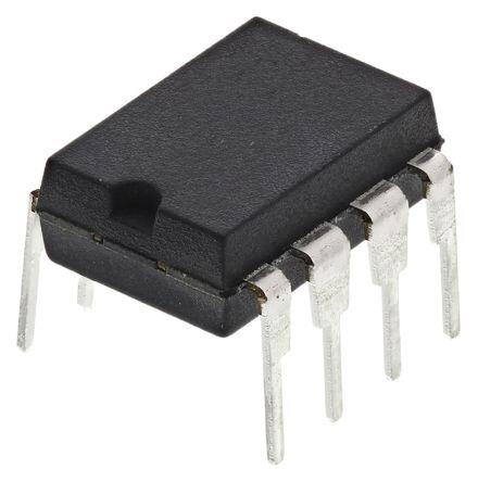
| 描述 | IC OPAMP INSTR 70KHZ 8DIP仪表放大器 Precision G = 100 Instrumentation Amp |
| 产品分类 | Linear - Amplifiers - Instrumentation, OP Amps, Buffer Amps集成电路 - IC |
| 品牌 | Texas Instruments |
| 产品手册 | http://www.ti.com/litv/sbos016 |
| 产品图片 |
|
| rohs | 符合RoHS无铅 / 符合限制有害物质指令(RoHS)规范要求 |
| 产品系列 | 放大器 IC,仪表放大器,Texas Instruments INA131BP- |
| 数据手册 | |
| 产品型号 | INA131BP |
| 产品目录页面 | |
| 产品种类 | 仪表放大器 |
| 供应商器件封装 | 8-PDIP |
| 共模抑制比—最小值 | 110 dB |
| 包装 | 管件 |
| 单位重量 | 528.600 mg |
| 单电源电压 | 4.5 V to 36 V |
| 压摆率 | 0.7 V/µs |
| 双重电源电压 | +/- 15 V |
| 可用增益调整 | 100 V/V |
| 商标 | Texas Instruments |
| 增益带宽生成 | 70 kHz |
| 增益带宽积 | - |
| 安装类型 | 通孔 |
| 安装风格 | Through Hole |
| 封装 | Tube |
| 封装/外壳 | 8-DIP(0.300",7.62mm) |
| 封装/箱体 | PDIP-8 |
| 工作温度 | -40°C ~ 85°C |
| 工作电源电压 | 4.5 V to 36 V |
| 工厂包装数量 | 50 |
| 放大器类型 | 仪表 |
| 最大工作温度 | + 85 C |
| 最大输入电阻 | 10000 MOhms |
| 最小工作温度 | - 40 C |
| 标准包装 | 50 |
| 电压-电源,单/双 (±) | 4.5 V ~ 36 V, ±2.25 V ~ 18 V |
| 电压-输入失调 | 10µV |
| 电流-电源 | 2.2mA |
| 电流-输入偏置 | 500pA |
| 电流-输出/通道 | 20mA |
| 电源电流 | 3 mA |
| 电路数 | 1 |
| 系列 | INA131 |
| 输入偏压电流—最大 | 2 nA |
| 输入补偿电压 | 50 uV |
| 输出类型 | - |
| 通道数量 | 1 Channel |


- 商务部:美国ITC正式对集成电路等产品启动337调查
- 曝三星4nm工艺存在良率问题 高通将骁龙8 Gen1或转产台积电
- 太阳诱电将投资9.5亿元在常州建新厂生产MLCC 预计2023年完工
- 英特尔发布欧洲新工厂建设计划 深化IDM 2.0 战略
- 台积电先进制程称霸业界 有大客户加持明年业绩稳了
- 达到5530亿美元!SIA预计今年全球半导体销售额将创下新高
- 英特尔拟将自动驾驶子公司Mobileye上市 估值或超500亿美元
- 三星加码芯片和SET,合并消费电子和移动部门,撤换高东真等 CEO
- 三星电子宣布重大人事变动 还合并消费电子和移动部门
- 海关总署:前11个月进口集成电路产品价值2.52万亿元 增长14.8%


PDF Datasheet 数据手册内容提取
® INA131 INA131 Precision G = 100 INSTRUMENTATION AMPLIFIER FEATURES DESCRIPTION l LOW OFFSET VOLTAGE: 50m V max The INA131 is a low cost, general purpose G = 100 l LOW DRIFT: 0.25m V/(cid:176) C max instrumentation amplifier offering excellent accuracy. Its 3-op amp design and small size make it ideal for l LOW INPUT BIAS CURRENT: 2nA max a wide range of applications. l HIGH COMMON-MODE REJECTION: On-chip laser trimmed resistors accurately set a fixed 110dB min gain of 100. The INA131 is laser trimmed to achieve l INPUT OVERVOLTAGE PROTECTION: very low offset voltage (50m V max), drift (0.25m V/(cid:176) C – 40V max), and high CMR (110dB min). Internal input l WIDE SUPPLY RANGE: – 2.25 to – 18V protection can withstand up to – 40V inputs without l LOW QUIESCENT CURRENT: 3mA damage. l 8-PIN PLASTIC DIP The INA131 is available in a 8-pin plastic DIP. They are specified over the –40(cid:176) C to +85(cid:176) C temperature range. APPLICATIONS l BRIDGE AMPLIFIER l THERMOCOUPLE AMPLIFIER l RTD SENSOR AMPLIFIER l MEDICAL INSTRUMENTATION l DATA ACQUISITION V+ 7 – 2 Over-Voltage INA131 V IN Protection A 1 5kW 25kW 1 25kW 6 + – 2.63kW A3 VO = 100 (VIN – VIN) 8 25kW 5 A Ref V+ 3 Over-Voltage 2 5kW 25kW IN Protection 4 DIP V– International Airport Industrial Park • Mailing Address: PO Box 11400, Tucson, AZ 85734 • Street Address: 6730 S. Tucson Blvd., Tucson, AZ 85706 • Tel: (520) 746-1111 • Twx: 910-952-1111 Internet: http://www.burr-brown.com/ • FAXLine: (800) 548-6133 (US/Canada Only) • Cable: BBRCORP • Telex: 066-6491 • FAX: (520) 889-1510 • Immediate Product Info: (800) 548-6132 ©1992 Burr-Brown Corporation PDS-1144E Printed in U.S.A. March, 1998 SBOS016
SPECIFICATIONS At T = +25(cid:176)C, V = – 15V, R = 2kW , unless otherwise noted. A S L INA131BP INA131AP PARAMETER CONDITIONS MIN TYP MAX MIN TYP MAX UNITS INPUT Offset Voltage, RTI Initial T = +25(cid:176)C – 10 – 50 – 25 – 125 m V A vs Temperature T = T to T – 0.1 – 0.25 – 0.25 – 1 m V/(cid:176)C A MIN MAX vs Power Supply V = – 2.25V to – 18V 0.5 3 [ [ m V/V S Long-Term Stability 0.2 [ m V/mo Impedance, Differential 1010 || 6 [ W || pF Common-Mode 1010 || 6 [ W || pF Input Common-Mode Range – 11 – 13.5 [ [ V Safe Input Voltage – 40 [ V Common-Mode Rejection V = – 10V, D R = 1kW 110 120 106 110 dB CM S BIAS CURRENT – 0.5 – 2 [ – 5 nA vs Temperature – 8 [ pA/(cid:176)C OFFSET CURRENT – 0.5 – 2 [ – 5 nA vs Temperature – 8 [ pA/(cid:176)C NOISE VOLTAGE, RTI R = 0W S f = 10Hz 16 [ nV/(cid:214) Hz f = 100Hz 12 [ nV/(cid:214) Hz f = 1kHz 12 [ nV/(cid:214) Hz f = 10kHz 12 [ nV/(cid:214) Hz f = 0.1Hz to 10Hz 0.4 [ m Vp-p B Noise Current f = 10Hz 0.4 [ pA/(cid:214) Hz f= 1kHz 0.2 [ pA/(cid:214) Hz f = 0.1Hz to 100Hz 18 [ pAp-p B GAIN Gain Error(1) – 0.01 – 0.024 [ – 0.1 % Resistor Value(2) – 10 – 40 [ [ % Gain vs Temperature – 5 – 10 [ – 20 ppm/(cid:176)C Nonlinearity – 0.0003 – 0.002 [ – 0.004 % of FSR OUTPUT Voltage I = 5mA, T to T – 13.5 – 13.7 [ [ V O MIN MAX V = – 11.4V, R = 2kW – 10 10.5 [ [ V S L V = – 2.25V, R = 2kW – 1 1.5 [ [ V S L Load Capacitance, max Stable Operation 1000 [ pF Short Circuit Current +20/–15 [ mA FREQUENCY RESPONSE Bandwidth, –3dB 70 [ kHz Slew Rate V = – 10V 0.3 0.7 [ [ V/m s O Settling Time, 0.01% 100 [ m s Overload Recovery 50% Overdrive 20 [ m s POWER SUPPLY Voltage Range – 2.25 – 15 – 18 [ [ [ V Current V = 0V – 2.2 – 3 [ [ mA IN TEMPERATURE RANGE Specification –40 85 [ [ (cid:176)C Operating –40 125 [ [ (cid:176)C q 100 [ (cid:176)C/W JA [ Specification same as INA131BP. NOTES: (1) R = 10kW . (2) Absolute value of internal gain-setting resistors. (Gain depends on resistor ratios.) L The information provided herein is believed to be reliable; however, BURR-BROWN assumes no responsibility for inaccuracies or omissions. BURR-BROWN assumes no responsibility for the use of this information, and all use of such information shall be entirely at the user’s own risk. Prices and specifications are subject to change without notice. No patent rights or licenses to any of the circuits described herein are implied or granted to any third party. BURR-BROWN does not authorize or warrant any BURR-BROWN product for use in life support devices and/or systems. ® INA131 2
PIN CONFIGURATION ABSOLUTE MAXIMUM RATINGS(1) Top View P-Package/8-Pin DIP Supply Voltage..................................................................................– 18V Input Voltage Range..........................................................................– 40V Output Short Circuit (to ground)..............................................Continuous RG 1 8 RG Operating Temperature..................................................–40(cid:176)C to +125(cid:176)C V– 2 7 V+ Storage Temperature.....................................................–40(cid:176)C to +125(cid:176)C IN Junction Temperature....................................................................+150(cid:176)C V+ 3 6 V Lead Temperature (soldering –10s)..............................................+300(cid:176)C IN O NOTE: (1) Stresses above these ratings may cause permanent damage. V– 4 5 Ref ELECTROSTATIC DISCHARGE SENSITIVITY PACKAGE/ORDERING INFORMATION This integrated circuit can be damaged by ESD. Burr-Brown PACKAGE recommends that all integrated circuits be handled with ap- DRAWING TEMPERATURE PRODUCT PACKAGE NUMBER(1) RANGE propriate precautions. Failure to observe proper handling and INA131AP 8-Pin Plastic DIP 006 –40(cid:176)C to +85(cid:176)C installation procedures can cause damage. INA131BP 8-Pin Plastic DIP 006 –40(cid:176)C to +85(cid:176)C ESD damage can range from subtle performance degradation NOTE: (1) For detailed drawing and dimension table, please see end of data to complete device failure. Precision integrated circuits may sheet, or Appendix C of Burr-Brown IC Data Book. be more susceptible to damage because very small parametric changes could cause the device not to meet its published specifications. ® 3 INA131
TYPICAL PERFORMANCE CURVES At 25(cid:176)C, V = – 15V, unless otherwise noted. S GAIN vs FREQUENCY COMMON-MODE REJECTION vs FREQUENCY 60 140 B) 120 d 40 on ( 100 cti B) eje 80 d R ain ( 20 ode 60 G M n- 0 mmo 40 o C 20 –20 0 100 1k 10k 100k 1M 10M 10 100 1k 10k 100k 1M Frequency (Hz) Frequency (Hz) INPUT COMMON-MODE VOLTAGE RANGE POWER SUPPLY REJECTION vs OUTPUT VOLTAGE vs FREQUENCY 15 140 n-Mode Voltage (V) 1500 A3+ L– iO mOuiutteptpduu tb tSyw AiVVn1DDVg//C22M ––++ + LOimuAtiVpt3eO u+dt SbOywu Atinp2gut upply Rejection (dB) 1186200000 PPPPoooossssiiiittttiiiivvvveeee SSSSuuuuppppppppllllyyyy Negative Supply o –5 Swing Limit Swing Limit S Comm –10 – LOimutipteudt Sbyw Ain2g –L iOmuittepdu tb Syw Ain1g Power 4200 –15 0 –15 –10 –5 0 5 10 15 10 100 1k 10k 100k 1M Output Voltage (V) Frequency (Hz) INPUT- REFERRED NOISE VOLTAGE vs FREQUENCY OFFSET VOLTAGE WARM-UP vs TIME 100 6 z) H (cid:214)Referred Noise Voltage (nV/ 10 Offset Voltage Change (µV) ––42024 ut- p n I 1 –6 1 10 100 1k 10k 0 15 30 45 60 75 90 105 120 Frequency (Hz) Time from Power Supply Turn-on (s) ® INA131 4
TYPICAL PERFORMANCE CURVES (CONT) At 25(cid:176)C, V = – 15V, unless otherwise noted. S INPUT BIAS AND INPUT OFFSET CURRENT INPUT BIAS CURRENT vs TEMPERATURE vs INPUT VOLTAGE 2 3 A) n nt ( 2 e Curr 1 mA) s and Input Offset –01 ±IIBOS nput Bias Current ( –101 Co(|mIBm1| o+n |-IMB2o|)de Differential Mode a I Bi –2 ut p n I –2 –3 –40 –15 10 35 60 85 –45 –30 –15 0 15 30 45 Temperature (°C) Differential Overload Voltage (V) MAXIMUM OUTPUT SWING vs FREQUENCY SLEW RATE vs TEMPERATURE 32 1.2 28 V) 1.0 e ( 24 ud s) plit 20 V/µ 0.8 Am e ( k 16 at a R ak-to-Pe 128 Slew 0.6 e 0.4 P 4 0 0.2 10 100 1k 10k 100k 1M –75 –50 –25 0 25 50 75 100 125 Frequency (Hz) Temperature (°C) OUTPUT CURRENT LIMIT vs TEMPERATURE QUIESCENT CURRENT vs TEMPERATURE 30 2.8 mA) 25 A) 2.6 Circuit Current ( 20 +|ICL| scent Current (m 22..42 hort 15 Quie S –|I | 2.0 CL 10 1.8 –40 –15 10 35 60 85 –75 –50 –25 0 25 50 75 100 125 Temperature (°C) Temperature (°C) ® 5 INA131
TYPICAL PERFORMANCE CURVES (CONT) At 25(cid:176)C, V = – 15V, unless otherwise noted. S QUIESCENT CURRENT AND POWER DISSIPATION vs POWER SUPPLY VOLTAGE POSITIVE SIGNAL SWING vs TEMPERATUE (R = 2kW ) L 2.6 120 16 V = ±15V S 14 2.5 100 A) W) 12 ent (m 2.4 Power Dissipation 80 on (m ge (V) 10 VS = ±11.4V Quiescent Curr 22..32 Quiescent Current 6400 Power Dissipati Output Volta 864 2.1 20 V = ±2.25V 2 S 2.0 0 0 0 ±3 ±6 ±9 ±12 ±15 ±18 –75 –50 –25 0 25 50 75 100 125 Power Supply Voltage (V) Temperature (°C) NEGATIVE SIGNAL SWING vs TEMPERATUE (R = 2kW ) LARGE SIGNAL RESPONSE, G = 100 L –16 V = ±15V S –14 –12 +10V V) VS = ±11.4V e ( –10 g a olt –8 0 V ut p –6 ut O –4 –10V V = ±2.25V S –2 0 –75 –50 –25 0 25 50 75 100 125 Temperature (°C) SMALL SIGNAL RESPONSE, G = 100 INPUT-REFERRED NOISE, 0.1 to 10Hz +200mV 0 0.1m V/div –200mV 1s/div ® INA131 6
APPLICATION INFORMATION device. Absolute accuracy of the internal values is – 40%. The nominal gain with an external R resistor can be G Figure 1 shows the basic connections required for operation calculated by: of the INA131. Applications with noisy or high impedance power supplies may require decoupling capacitors close to G=100+ 250kW (1) the device pins as shown. R G The output is referred to the output reference (Ref) terminal which is normally grounded. This must be a low-impedance Where: R is the external gain resistor. connection to assure good common-mode rejection. A resis- G Accuracy of the 250kW term is – 40%. tance of 5W in series with the Ref pin will cause a device with 110dB CMR to degrade to approximately 106dB CMR. The stability and temperature drift of the external gain setting resistor, R also affects gain. R ’s contribution to SETTING THE GAIN G, G gain accuracy and drift can be directly inferred from the No external resistors are required for G = 100. On-chip gain equation (1). laser-trimmed resistors set the gain, providing excellent gain accuracy and temperature stability. Gain is distributed be- tween the input and output stages of the INA131. Bandwidth NOISE PERFORMANCE is increased by approximately five times (compared to the The INA131 provides very low noise in most applications. INA114 in G = 100). Input common-mode range is also For differential source impedances less than 1kW , the improved (see “Input Common-Mode Range”). INA103 may provide lower noise. For source impedances greater than 50kW , the INA111 FET-Input Instrumentation Although the INA131 is primarily intended for fixed Amplifier may provide lower noise. G = 100 applications, the gain can be increased by connect- ing an external resistor to the R pins. The internal resistors Low frequency noise of the INA131 is approximately G are trimmed for precise ratios, not to absolute values, so the 0.4m Vp-p measured from 0.1 to 10Hz. This is approxi- influence of an external resistor will vary from device to mately one-tenth the noise of state-of-the-art chopper-stabi- lized amplifiers. V+ 0.1µF Pin numbers are for DIP packages. 7 INA131 – 2 Over-Voltage V IN Protection A 1 5kW 25kW 1 25kW V = 100 • (V+ – V–) O IN IN 6 2.63kW A3 + 8 25kW Load VO – 5 A + 3 Over-Voltage 2 V 5kW 25kW IN Protection 4 0.1µF Also drawn in simplified form: V– V– IN INA131 V O V+ Ref IN FIGURE 1. Basic Connections. ® 7 INA131
OFFSET TRIMMING The INA131 is laser trimmed for very low offset voltage and Microphone, drift. Most applications require no external offset adjust- Hydrophone INA131 ment. Figure 2 shows an optional circuit for trimming the etc. output offset voltage. The voltage applied to Ref terminal is summed at the output. Low impedance must be maintained 47kW 47kW at this node to assure good common-mode rejection. This is achieved by buffering trim voltage with an op amp as shown. Thermocouple INA131 – V+ VIN VO INA131 + 100µA 10kW VIN Ref 1/2 REF200 100W OPA177 ±10mV 10kW INA131 Adjustment Range 100W Center-tap provides 100µA bias current return. 1/2 REF200 FIGURE 3. Providing an Input Common-Mode Current Path. V– FIGURE 2. Optional Trimming of Output Offset Voltage. INA114 and other unity output gain instrumentation ampli- fiers, the INA131 provides several additional volts of input INPUT BIAS CURRENT RETURN PATH common-mode range with full output voltage swing. See the typical performance curve “Input Common-Mode Range vs The input impedance of the INA131 is extremely high— approximately 1010W . However, a path must be provided for Output Voltage”. the input bias current of both inputs. This input bias current Input-overload often produces an output voltage that appears is typically less than – 1nA (it can be either polarity due to normal. For example, an input voltage of +20V on one input cancellation circuitry). High input impedance means that and +40V on the other input will obviously exceed the linear this input bias current changes very little with varying input common-mode range of both input amplifiers. Since both voltage. input amplifiers are saturated to the nearly the same output voltage limit, the difference voltage measured by the output Input circuitry must provide a path for this input bias current amplifier will be near zero. The output of the INA131 will if the INA131 is to operate properly. Figure 3 shows various be near 0V even though both inputs are overloaded. provisions for an input bias current path. Without a bias current return path, the inputs will float to a potential which exceeds the common-mode range of the INA131 and the INPUT PROTECTION input amplifiers will saturate. If the differential source resis- The inputs of the INA131 are individually protected for tance is low, bias current return path can be connected to one voltages up to – 40V. For example, a condition of –40V on input (see thermocouple example in Figure 3). With higher one input and +40V on the other input will not cause source impedance, using two resistors provides a balanced damage. Internal circuitry on each input provides low series input with possible advantages of lower input offset voltage impedance under normal signal conditions. To provide due to bias current and better common-mode rejection. equivalent protection, series input resistors would contribute excessive noise. If the input is overloaded, the protection INPUT COMMON-MODE RANGE circuitry limits the input current to a safe value (approxi- mately 1.5mA). The typical performance curve “Input Bias The linear common-mode range of the input op amps of the INA131 is approximately – 13.75V (or 1.25V from the Current vs Input Voltage” shows this input current limit behavior. The inputs are protected even if no power supply power supplies). As the output voltage increases, however, voltage is present. the linear input range is limited by the output voltage swing of the input amplifiers, A and A. The 5V/V output stage 1 2 gain of the INA131 reduces this effect. Compared to the ® INA131 8
VI–N 1MW VO V+ 1MW INA131 IN Ref Shield is driven at the common-mode potential. 100W Common-mode resistors have OPA602 approximately 0.1% effect on gain. FIGURE 4. Shield Driver Circuit. V+ V+ REF200 Equal line resistance here creates 100µA a small common-mode voltage which is rejected by INA131. 1 V O RTD INA131 2 Ref R Z 3 Resistance in this line causes VO = 0V at RRTD = RZ a small common-mode voltage which is rejected by INA131. FIGURE 5. RTD Temperature Measurement Circuit. V+ 2 10.0V 6 REF102 R 1 R 27kW 4 80.6kW 4 1N4148 (2) (1) R2 R7 Cu 5.23kW 1MW V O INA131 K Cu Ref R3 R5 100W 50W R 6 SEEBECK 100W ISA COEFFICIENT R R TYPE MATERIAL (m V/(cid:176)C) (R = 1200W ) (R + R 4= 100W ) Zero Adj 3 5 6 E Chromel 58.5 3.48kW 56.2kW Constantan J Iron 50.2 4.12kW 64.9kW Constantan K Chromel 39.4 5.23kW 80.6kW Alumel T Copper 38.0 5.49kW 84.5kW Constantan NOTES: (1) –2.1mV/(cid:176)C at 200m A. (2) R provides down-scale burn-out indication. 7 FIGURE 6. Thermocouple Amplifier with Cold Junction Compensation. ® 9 INA131
+10V – R I = 1 0 0 • VIN O R VIN INA131 + Ref Bridge I B V O INA131 A1 IO Ref Load FIGURE 7. Bridge Transducer Amplifier. A I Error 1 B OPA177 – 1.5nA OPA602 1pA OPA128 75fA – V O VIN INA131 + FIGURE 9. Differential Voltage to Current Converter. Ref R C 1 1 1MW 0.1µF f = 1 OPA602 –3dB 2p R1C1 = 1.59Hz FIGURE 8. AC-Coupled Instrumentation Amplifier. ® INA131 10
IMPORTANT NOTICE Texas Instruments and its subsidiaries (TI) reserve the right to make changes to their products or to discontinue any product or service without notice, and advise customers to obtain the latest version of relevant information to verify, before placing orders, that information being relied on is current and complete. All products are sold subject to the terms and conditions of sale supplied at the time of order acknowledgment, including those pertaining to warranty, patent infringement, and limitation of liability. TI warrants performance of its semiconductor products to the specifications applicable at the time of sale in accordance with TI’s standard warranty. Testing and other quality control techniques are utilized to the extent TI deems necessary to support this warranty. Specific testing of all parameters of each device is not necessarily performed, except those mandated by government requirements. Customers are responsible for their applications using TI components. In order to minimize risks associated with the customer’s applications, adequate design and operating safeguards must be provided by the customer to minimize inherent or procedural hazards. TI assumes no liability for applications assistance or customer product design. TI does not warrant or represent that any license, either express or implied, is granted under any patent right, copyright, mask work right, or other intellectual property right of TI covering or relating to any combination, machine, or process in which such semiconductor products or services might be or are used. TI’s publication of information regarding any third party’s products or services does not constitute TI’s approval, warranty or endorsement thereof. Copyright 2000, Texas Instruments Incorporated