ICGOO在线商城 > 集成电路(IC) > 线性 - 放大器 - 仪表,运算放大器,缓冲器放大器 > OPA4376AIPWR

 Datasheet下载
- 型号: OPA4376AIPWR
- 制造商: Texas Instruments
- 库位|库存: xxxx|xxxx
- 要求:
| 数量阶梯 | 香港交货 | 国内含税 |
| +xxxx | $xxxx | ¥xxxx |
查看当月历史价格
查看今年历史价格
OPA4376AIPWR产品简介:
ICGOO电子元器件商城为您提供OPA4376AIPWR由Texas Instruments设计生产,在icgoo商城现货销售,并且可以通过原厂、代理商等渠道进行代购。 OPA4376AIPWR价格参考。Texas InstrumentsOPA4376AIPWR封装/规格:线性 - 放大器 - 仪表,运算放大器,缓冲器放大器, General Purpose Amplifier 4 Circuit Rail-to-Rail 14-TSSOP。您可以下载OPA4376AIPWR参考资料、Datasheet数据手册功能说明书,资料中有OPA4376AIPWR 详细功能的应用电路图电压和使用方法及教程。
OPA4376AIPWR是德州仪器(Texas Instruments)推出的一款高精度、低功耗、零漂移运算放大器,属于线性放大器中的精密运算放大器类别。该器件采用RRIO( Rail-to-Rail Input/Output)设计,具有极低的输入失调电压和温漂,适用于对信号精度要求较高的应用场景。

典型应用包括:便携式医疗设备(如心电图仪、血糖仪)、工业传感器信号调理(如压力、温度、称重传感器)、高分辨率数据采集系统、电池供电设备以及精密测量仪器。其低噪声、低功耗特性使其非常适合在电源受限或需要长期稳定工作的系统中使用。

此外,OPA4376AIPWR为四通道设计,封装为TSSOP-14,有助于节省PCB空间,提高系统集成度。广泛应用于模拟前端信号放大、滤波、电流检测和电压缓冲等电路中。由于具备出色的直流精度和长期稳定性,也常用于自动化测试设备和工业控制中的模拟信号处理模块。

总之,OPA4376AIPWR凭借其高精度、低功耗和小型化优势,特别适合对性能和可靠性要求严苛的精密模拟信号处理场景。
| 参数 | 数值 |
| -3db带宽 | - |
| 产品目录 | 集成电路 (IC)半导体 |
| 描述 | IC OPAMP GP 5.5MHZ RRO 14TSSOP运算放大器 - 运放 Precision Lo Noise Lo Quiescent Current |
| 产品分类 | Linear - Amplifiers - Instrumentation, OP Amps, Buffer Amps集成电路 - IC |
| 品牌 | Texas Instruments |
| 产品手册 | |
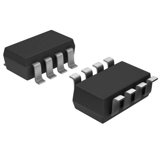
| 产品图片 |
|
| rohs | 符合RoHS无铅 / 符合限制有害物质指令(RoHS)规范要求 |
| 产品系列 | 放大器 IC,运算放大器 - 运放,Texas Instruments OPA4376AIPWRe-trim™ |
| 数据手册 | |
| 产品型号 | OPA4376AIPWR |
| 产品目录页面 | |
| 产品种类 | 运算放大器 - 运放 |
| 供应商器件封装 | 14-TSSOP |
| 共模抑制比—最小值 | 76 dB |
| 关闭 | No Shutdown |
| 其它名称 | 296-22565-1 |
| 包装 | 剪切带 (CT) |
| 压摆率 | 2 V/µs |
| 商标 | Texas Instruments |
| 增益带宽生成 | 5.5 MHz |
| 增益带宽积 | 5.5MHz |
| 安装类型 | 表面贴装 |
| 安装风格 | SMD/SMT |
| 封装 | Reel |
| 封装/外壳 | 14-TSSOP(0.173",4.40mm 宽) |
| 封装/箱体 | TSSOP-14 |
| 工作温度 | -40°C ~ 125°C |
| 工作电源电压 | 2.2 V to 5.5 V |
| 工厂包装数量 | 2000 |
| 技术 | CMOS |
| 放大器类型 | 通用 |
| 最大工作温度 | + 125 C |
| 最小工作温度 | - 40 C |
| 标准包装 | 1 |
| 电压-电源,单/双 (±) | 2.2 V ~ 5.5 V, ±1.1 V ~ 2.75 V |
| 电压-输入失调 | 5µV |
| 电流-电源 | 760µA |
| 电流-输入偏置 | 0.2pA |
| 电流-输出/通道 | 50mA |
| 电源电流 | 950 uA |
| 电路数 | 4 |
| 系列 | OPA4376 |
| 设计资源 | http://www.digikey.com/product-highlights/cn/zh/texas-instruments-webench-design-center/3176 |
| 转换速度 | 2 V/us |
| 输入偏压电流—最大 | 10 pA |
| 输入参考电压噪声 | 7.5 nV |
| 输入补偿电压 | 25 uV |
| 输出类型 | 满摆幅 |
| 通道数量 | 4 Channel |


- 商务部:美国ITC正式对集成电路等产品启动337调查
- 曝三星4nm工艺存在良率问题 高通将骁龙8 Gen1或转产台积电
- 太阳诱电将投资9.5亿元在常州建新厂生产MLCC 预计2023年完工
- 英特尔发布欧洲新工厂建设计划 深化IDM 2.0 战略
- 台积电先进制程称霸业界 有大客户加持明年业绩稳了
- 达到5530亿美元!SIA预计今年全球半导体销售额将创下新高
- 英特尔拟将自动驾驶子公司Mobileye上市 估值或超500亿美元
- 三星加码芯片和SET,合并消费电子和移动部门,撤换高东真等 CEO
- 三星电子宣布重大人事变动 还合并消费电子和移动部门
- 海关总署:前11个月进口集成电路产品价值2.52万亿元 增长14.8%


PDF Datasheet 数据手册内容提取
Product Sample & Technical Tools & Support & Reference Folder Buy Documents Software Community Design OPA376,OPA2376,OPA4376 SBOS406G–JUNE2007–REVISEDDECEMBER2015 OPAx376 Low-Noise, Low Quiescent Current, Precision Operational Amplifier e-trim Series 1 Features 3 Description • LowNoise:7.5nV/√Hzat1kHz The OPA376 family represents a new generation of 1 low-noise operational amplifiers with e-trim™, offering • 0.1Hzto10HzNoise:0.8μV PP outstanding dc precision and ac performance. Rail-to- • QuiescentCurrent:760 μA(typical) rail input and output, low offset (25 μV, maximum), • LowOffsetVoltage:5μV(typ) low noise (7.5 nV/√Hz), quiescent current of 950 μA (maximum), and a 5.5-MHz bandwidth make this part • GainBandwidthProduct:5.5MHz very attractive for a variety of precision and portable • Rail-to-RailInputandOutput applications. In addition, this device has a reasonably • Single-SupplyOperation wide supply range with excellent PSRR, making it attractive for applications that run directly from • SupplyVoltage:2.2Vto5.5V batterieswithoutregulation. • Space-SavingPackages: The OPA376 (single version) is available in – SC70,SOT-23,DSBGA,VSSOP,TSSOP MicroSIZE SC70-5, SOT-23-5, and SOIC-8 packages. The OPA2376 (dual) is offered in the 2 Applications DSBGA-8, VSSOP-8, and SOIC-8 packages. The • ADCBuffer OPA4376 (quad) is offered in a TSSOP-14 package. All versions are specified for operation from –40°C to • AudioEquipment +125°C. • MedicalInstrumentation • HandheldTestEquipment DeviceInformation(1) • ActiveFiltering PARTNUMBER PACKAGE BODYSIZE(NOM) • SensorSignalConditioning SOIC(8) 4.90mm×3.91mm OPA376 SOT-23(5) 2.90mm×1.60mm SC70(5) 2.00mm×1.25mm SOIC(8) 4.90mm×3.91mm OPA2376 VSSOP(8) 3.00mm×3.00mm DSBGA(8) 1.30mm×2.30mm OPA4376 TSSOP(14) 5.00mm×4.40mm (1) Forallavailablepackages,seethepackageoptionaddendum attheendofthedatasheet. InputNoiseVoltageSpectralDensity OffsetVoltageProductionDistribution 100 )z H Ö V/ n n o e ( ati ois 10 pul N o e P g a olt V 1 1 10 100 1k 10k 100k 5.02.50.07.55.02.50.07.55.02.50 2.55.07.50.02.55.07.50.02.55.0 2221111--- 1111222 Frequency (Hz) ------- Offset Voltage (mV) 1 An IMPORTANT NOTICE at the end of this data sheet addresses availability, warranty, changes, use in safety-critical applications, intellectualpropertymattersandotherimportantdisclaimers.PRODUCTIONDATA.
OPA376,OPA2376,OPA4376 SBOS406G–JUNE2007–REVISEDDECEMBER2015 www.ti.com Table of Contents 1 Features.................................................................. 1 7.4 DeviceFunctionalModes........................................16 2 Applications........................................................... 1 8 ApplicationandImplementation........................ 17 3 Description............................................................. 1 8.1 ApplicationInformation............................................17 4 RevisionHistory..................................................... 2 8.2 TypicalApplication .................................................20 5 PinConfigurationandFunctions......................... 3 9 PowerSupplyRecommendations...................... 21 6 Specifications......................................................... 6 10 Layout................................................................... 21 6.1 AbsoluteMaximumRatings......................................6 10.1 LayoutGuidelines.................................................21 6.2 ESDRatings..............................................................6 10.2 LayoutExample....................................................22 6.3 RecommendedOperatingConditions.......................6 11 DeviceandDocumentationSupport................. 23 6.4 ThermalInformation:OPA376..................................7 11.1 DeviceSupport......................................................23 6.5 ThermalInformation:OPA2376................................7 11.2 RelatedDocumentation .......................................23 6.6 ThermalInformation:OPA4376................................7 11.3 RelatedLinks........................................................24 6.7 ElectricalCharacteristics..........................................8 11.4 CommunityResources..........................................24 6.8 TypicalCharacteristics............................................10 11.5 Trademarks...........................................................24 7 DetailedDescription............................................ 14 11.6 ElectrostaticDischargeCaution............................24 7.1 Overview.................................................................14 11.7 Glossary................................................................24 7.2 FunctionalBlockDiagram.......................................14 12 Mechanical,Packaging,andOrderable Information........................................................... 25 7.3 FeatureDescription.................................................14 4 Revision History NOTE:Pagenumbersforpreviousrevisionsmaydifferfrompagenumbersinthecurrentversion. ChangesfromRevisionF(March2013)toRevisionG Page • AddedESDRatings,ThermalInformation,RecommendedOperatingConditions,PowerSupplyRecommendations, andDeviceandDocumentationSupportsections;existingsectionsmayhavemoved........................................................ 1 • ChangedWCSPtoDSBGAandMSOPtoVSSOPthroughoutdatasheet........................................................................... 1 • ChangeddimensionsshowninYZDpackagepinoutfigure................................................................................................... 4 ChangesfromRevisionE(January2013)toRevisionF Page • Changedunit(typo)forQuiescentCurrentfeaturebullet....................................................................................................... 1 • ChangedTSSOP-14pinoutforOPA4376.............................................................................................................................. 5 ChangesfromRevisionD(August2010)toRevisionE Page • Changedrail-to-railfeaturebullettoshowinputandoutput................................................................................................... 1 • Changeddescriptiontexttoshowrail-to-railinputandoutput............................................................................................... 1 ChangesfromRevisionC(October2008)toRevisionD Page • UpdatedformatofElectricalCharacteristicstable................................................................................................................. 8 • UpdatedFigure11................................................................................................................................................................ 11 2 SubmitDocumentationFeedback Copyright©2007–2015,TexasInstrumentsIncorporated ProductFolderLinks:OPA376 OPA2376 OPA4376
OPA376,OPA2376,OPA4376 www.ti.com SBOS406G–JUNE2007–REVISEDDECEMBER2015 5 Pin Configuration and Functions OPA376:DBVPackage 5-PinSOT23 OPA376:DCKPackage TopView 5-PinSC70-5 TopView OUT 1 5 V+ +IN 1 5 V+ V- 2 V- 2 +IN 3 4 -IN -IN 3 4 OUT OPA376:DPackage 8-PinSOIC TopView (1) (1) NC 1 8 NC -IN 2 - 7 V+ + +IN 3 6 OUT V- 4 5 NC(1) (1) NCdenotesnointernalconnection. PinFunctions:OPA376 PIN I/O DESCRIPTION NAME DBV DCK D +IN 3 1 3 I Inputsignal+ –IN 4 3 2 I Inputsignal– NC — — 1,5,8 — Noconnection OUT 1 4 6 O Outputsignal V+ 5 5 7 — Supplyvoltage+ V– 2 2 4 — Supplyvoltage– Copyright©2007–2015,TexasInstrumentsIncorporated SubmitDocumentationFeedback 3 ProductFolderLinks:OPA376 OPA2376 OPA4376
OPA376,OPA2376,OPA4376 SBOS406G–JUNE2007–REVISEDDECEMBER2015 www.ti.com OPA2376:DandDGKPackages OPA2376:YZDPackage 8-PinSOICand8-PinVSSOP 8-PinDSBGA TopView TopView OUT A 1 8 V+ +IN B D2 D1 V- -IN A 2 7 OUT B -IN B C2 C1 +INA 2.178 mm +IN A 3 6 -IN B OUTB B2 B1 -INA 2.118 mm V- 4 5 +IN B V+ A2 A1 OUTA 1.14 mm 1.08 mm (Bump-Side Down) PinFunctions:OPA2376 PIN DAND I/O DESCRIPTION NAME YZD DGK +INA 3 C1 I InputsignalA+ –INA 2 B1 I InputsignalA– +INB 5 D2 I InputsignalB+ –INB 6 C2 I InputsignalB– OUTA 1 A1 O OutputsignalA OUTB 7 B2 O OutputsignalB V+ 8 A2 — Supplyvoltage+ V– 4 D1 — Supplyvoltage– 4 SubmitDocumentationFeedback Copyright©2007–2015,TexasInstrumentsIncorporated ProductFolderLinks:OPA376 OPA2376 OPA4376
OPA376,OPA2376,OPA4376 www.ti.com SBOS406G–JUNE2007–REVISEDDECEMBER2015 OPA4376:PWPackage 14-PinTSSOP TopView OUT A 1 14 OUT D -IN A 2 13 -IN D +IN A 3 12 +IN D V+ 4 11 V- +IN B 5 10 +IN C -IN B 6 9 -IN C OUT B 7 8 OUT C PinFunctions:OPA4376 PIN I/O DESCRIPTION NAME PW +INA 3 I InputsignalA+ –INA 2 O InputsignalA– +INB 5 I InputsignalB+ –INB 6 O InputsignalB– +INC 10 I InputsignalC+ –INC 9 O InputsignalC– +IND 12 I InputsignalD+ –IND 13 O InputsignalD– OUTA 1 O OutputsignalA OUTB 7 O OutputsignalB OUTC 8 O OutputsignalC OUTD 14 O OutputsignalD V+ 4 — Supplyvoltage+ V– 11 — Supplyvoltage– Copyright©2007–2015,TexasInstrumentsIncorporated SubmitDocumentationFeedback 5 ProductFolderLinks:OPA376 OPA2376 OPA4376
OPA376,OPA2376,OPA4376 SBOS406G–JUNE2007–REVISEDDECEMBER2015 www.ti.com 6 Specifications 6.1 Absolute Maximum Ratings overoperatingfree-airtemperaturerange(unlessotherwisenoted)(1) MIN MAX UNIT Supply,V =(V+)–(V–) 7 V S Voltage Signalinputpin(2) (V–)–0.5 (V+)+0.5 V Signalinputpin(2) –10 10 mA Current Outputshort-circuit(3) Continuous Operatingrange,T –40 150 A Temperature Junction,T 150 °C J Storage,T –65 150 stg (1) StressesbeyondthoselistedunderAbsoluteMaximumRatingsmaycausepermanentdamagetothedevice.Thesearestressratings only,whichdonotimplyfunctionaloperationofthedeviceattheseoranyotherconditionsbeyondthoseindicatedunderRecommended OperatingConditions.Exposuretoabsolute-maximum-ratedconditionsforextendedperiodsmayaffectdevicereliability. (2) Inputterminalsarediode-clampedtothepower-supplyrails.Inputsignalsthatcanswingmorethan0.5Vbeyondthesupplyrailsshould becurrentlimitedto10mAorless. (3) Short-circuittoground,oneamplifierperpackage. 6.2 ESD Ratings VALUE UNIT Humanbodymodel(HBM),perANSI/ESDA/JEDECJS-001, allpins(1) ±4000 V Electrostaticdischarge Chargeddevicemodel(CDM),perJEDECspecification V (ESD) JESD22-C101,allpins(2) ±1000 Machinemodel ±200 (1) JEDECdocumentJEP155statesthat500-VHBMallowssafemanufacturingwithastandardESDcontrolprocess. (2) JEDECdocumentJEP157statesthat250-VCDMallowssafemanufacturingwithastandardESDcontrolprocess. 6.3 Recommended Operating Conditions overoperatingfree-airtemperaturerange(unlessotherwisenoted) MIN NOM MAX UNIT (V+)–(V–) Supplyvoltage 2.2(±1.1) 5.5(±2.75) V T Operatingtemperature –40 150 °C A 6 SubmitDocumentationFeedback Copyright©2007–2015,TexasInstrumentsIncorporated ProductFolderLinks:OPA376 OPA2376 OPA4376
OPA376,OPA2376,OPA4376 www.ti.com SBOS406G–JUNE2007–REVISEDDECEMBER2015 6.4 Thermal Information: OPA376 OPA376 THERMALMETRIC(1) DBV(SOT-23) DCK(SC70) D(SOIC) UNIT 5PINS 5PINS 8PINS R Junction-to-ambientthermalresistance 273.8 267.0 100.1 °C/W θJA R Junction-to-case(top)thermalresistance 126.8 80.9 42.4 °C/W θJC(top) R Junction-to-boardthermalresistance 85.9 54.8 41.0 °C/W θJB ψ Junction-to-topcharacterizationparameter 10.9 1.2 4.8 °C/W JT ψ Junction-to-boardcharacterizationparameter 84.9 54.1 40.3 °C/W JB R Junction-to-case(bottom)thermalresistance n/a n/a n/a °C/W θJC(bot) (1) Formoreinformationabouttraditionalandnewthermalmetrics,seetheSemiconductorandICPackageThermalMetricsapplication report,SPRA953. 6.5 Thermal Information: OPA2376 OPA2376 THERMALMETRIC(1) D(SOIC) DGK(VSSOP) YZD(DSBGA) UNIT 8PINS 8PINS 8PINS R Junction-to-ambientthermalresistance 111.1 171.2 119.2 °C/W θJA R Junction-to-case(top)thermalresistance 54.7 63.9 0.6 °C/W θJC(top) R Junction-to-boardthermalresistance 51.7 92.8 27.6 °C/W θJB ψ Junction-to-topcharacterizationparameter 10.5 9.2 4.0 °C/W JT ψ Junction-to-boardcharacterizationparameter 51.2 91.2 27.6 °C/W JB R Junction-to-case(bottom)thermalresistance n/a n/a n/a °C/W θJC(bot) (1) Formoreinformationabouttraditionalandnewthermalmetrics,seetheSemiconductorandICPackageThermalMetricsapplication report,SPRA953. 6.6 Thermal Information: OPA4376 OPA4376 THERMALMETRIC(1) PW UNIT 14PINS R Junction-to-ambientthermalresistance 107.8 °C/W θJA R Junction-to-case(top)thermalresistance 29.6 °C/W θJC(top) R Junction-to-boardthermalresistance 52.6 °C/W θJB ψ Junction-to-topcharacterizationparameter 1.5 °C/W JT ψ Junction-to-boardcharacterizationparameter 51.6 °C/W JB R Junction-to-case(bottom)thermalresistance n/a °C/W θJC(bot) (1) Formoreinformationabouttraditionalandnewthermalmetrics,seetheSemiconductorandICPackageThermalMetricsapplication report,SPRA953. Copyright©2007–2015,TexasInstrumentsIncorporated SubmitDocumentationFeedback 7 ProductFolderLinks:OPA376 OPA2376 OPA4376
OPA376,OPA2376,OPA4376 SBOS406G–JUNE2007–REVISEDDECEMBER2015 www.ti.com 6.7 Electrical Characteristics AtT =25°C,R =10kΩconnectedtoV /2,V =V /2,andV =V /2,unlessotherwisenoted. A L S CM S OUT S PARAMETER TESTCONDITIONS MIN TYP MAX UNIT OFFSETVOLTAGE VOS Inputoffsetvoltage 5 25 μV Inputoffsetvoltageversus TA=–40°Cto+85°C 0.26 1 μV/°C dVOS/dT temperature TA=–40°Cto+125°C 0.32 2 μV/°C TA=25°C,VS=2.2Vto5.5V,VCM<(V+)–1.3V 5 20 μV/V Inputoffsetvoltageversus PSRR powersupply TA=–40°Cto+125°C, 5 μV/V VS=2.2Vto5.5V,VCM<(V+)–1.3V Channelseparation,dc 0.5 mV/V (dual,quad) INPUTBIASCURRENT TA=25°C 0.2 10 pA IB Inputbiascurrent TA=–40°Cto+125°C SeeTypicalCharacteristics pA IOS Inputoffsetcurrent 0.2 10 pA NOISE Inputvoltagenoise f=0.1Hzto10Hz 0.8 μVPP en Inputvoltagenoisedensity f=1kHz 7.5 nV/√Hz in Inputcurrentnoise f=1kHz 2 fA/√Hz INPUTVOLTAGERANGE Common-modevoltage VCM range (V–)–0.1 (V+)+0.1 V Common-moderejection CMRR ratio (V–)<VCM<(V+)–1.3V 76 90 dB INPUTCAPACITANCE Differential 6.5 pF Common-mode 13 pF OPEN-LOOPGAIN 50mV<VO<(V+)–50mV,RL=10kΩ 120 134 dB AOL Open-loopvoltagegain 100mV<VO<(V+)–100mV,RL=2kΩ 120 126 dB FREQUENCYRESPONSECL=100pF,VS=5.5V GBW Gain-bandwidthproduct 5.5 MHz SR Slewrate G=1 2 V/μs To0.1%,2-Vstep,G=1 1.6 μs tS Settlingtime To0.01%,2-Vstep,G=1 2 μs Overloadrecoverytime VIN ×gain>VS 0.33 μs Totalharmonicdistortion+ THD+N noise VO=1VRMS,G=1,f=1kHz,RL=10kΩ 0.00027% 8 SubmitDocumentationFeedback Copyright©2007–2015,TexasInstrumentsIncorporated ProductFolderLinks:OPA376 OPA2376 OPA4376
OPA376,OPA2376,OPA4376 www.ti.com SBOS406G–JUNE2007–REVISEDDECEMBER2015 Electrical Characteristics (continued) AtT =25°C,R =10kΩconnectedtoV /2,V =V /2,andV =V /2,unlessotherwisenoted. A L S CM S OUT S PARAMETER TESTCONDITIONS MIN TYP MAX UNIT OUTPUT SC70-5,SOT23-5,SO-8, VSSOP-8,andTSSOP-14 10 20 mV TA=25°C,RL=10kΩ packagesonly DSBGApackageonly 20 30 mV Voltageoutputswingfrom TA=–40°Cto+125°C,RL=10kΩ 40 mV rail SC70-5,SOT23-5,SO-8, VSSOP-8,andTSSOP-14 40 50 mV TA=25°C,RL=2kΩ packagesonly DSBGApackageonly 50 60 mV TA=–40°Cto+125°C,RL=2kΩ 80 mV ISC Short-circuitcurrent +30,–50 mA CLOAD Capacitiveloaddrive SeeTypicalCharacteristics Open-loopoutput RO impedance 150 Ω POWERSUPPLY VS Specifiedvoltagerange 2.2 5.5 V Operatingvoltagerange 2to5.5 V IQ Qamuipelsifcieerntcurrentper TTAA==–2450°C°C,IOto=+102,5V°SC=5.5V,VCM<(V+)–1.3V 760 9501 mμAA TEMPERATURE Specifiedrange –40 125 °C Operatingrange –40 150 °C Copyright©2007–2015,TexasInstrumentsIncorporated SubmitDocumentationFeedback 9 ProductFolderLinks:OPA376 OPA2376 OPA4376
OPA376,OPA2376,OPA4376 SBOS406G–JUNE2007–REVISEDDECEMBER2015 www.ti.com 6.8 Typical Characteristics AtT =25°C,V =5V,R =10kΩconnectedtoV /2,V =V /2,andV =V /2,unlessotherwisenoted. A S L S CM S OUT S 160 0 120 V(+)Power-Supply Rejection Ratio 140 -20 B) B) 120 Gain -40 atio (d 100 Open-Loop Gain (d 10864200000 Phase -----6811100024000 Phase Margin ()° wer-Supply Rejection R 86420000 V(-)Power-Supply Rejection Ratio CRoemjecmtioonn- MRoadtioe 0 -160 Po -20 -180 0 0.1 1 10 100 1k 10k 100k 1M 10M 10 100 1k 10k 100k 1M 10M Frequency (Hz) Frequency (Hz) Figure1. Open-LoopGainandPhasevsFrequency Figure2. Power-SupplyandCommon-ModeRejectionRatio vsFrequency 160 dB) Open-Loop Gain (RL= 2kW) R ( 140 R S P p Gain and 120 Powe(rV-SSu=p p2l.y1 VR etoje 5ct.i5oVn) Ratio 00nV/div o 5 o L 100 n- e p O 80 -50 -25 0 25 50 75 100 125 150 Temperature (°C) 1s/div Figure3. Open-LoopGainandPower-SupplyRejection Figure4. 0.1-Hzto10-HzInputVoltageNoise RatiovsTemperature 100 1 %) VS= 5V, VCM= 2V, VOUT= 1VRMS e ( s Ö)Hz + Noi 0.1 V/ n e (n ortio ge Nois 10 nic Dist 0.01 Gain = 10V/V a o Volt arm 0.001 al H Gain = 1V/V Tot 1 0.0001 1 10 100 1k 10k 100k 10 100 1k 10k 100k Frequency (Hz) Frequency (Hz) Figure5. InputVoltageNoiseSpectralDensity Figure6. TotalHarmonicDistortion+NoisevsFrequency 10 SubmitDocumentationFeedback Copyright©2007–2015,TexasInstrumentsIncorporated ProductFolderLinks:OPA376 OPA2376 OPA4376
OPA376,OPA2376,OPA4376 www.ti.com SBOS406G–JUNE2007–REVISEDDECEMBER2015 Typical Characteristics (continued) AtT =25°C,V =5V,R =10kΩconnectedtoV /2,V =V /2,andV =V /2,unlessotherwisenoted. A S L S CM S OUT S 110 1000 B) d atio ( 100 A) 900 R m on 90 nt ( ejecti 80 Curre 800 Mode R 70 escent 700 n- ui o Q m 600 m 60 o C 50 500 -50 -25 0 25 50 75 100 125 150 -50 -25 0 25 50 75 100 125 150 Temperature (°C) Temperature (°C) Figure7. Common-ModeRejectionRatiovsTemperature Figure8. QuiescentCurrentvsTemperature 1000 50 75 V =±2.75V S 50 900 40 S A) I muiescent Current (A) 870000 IQ ISC+ 3200 hort-Circuit Current (m hort-Circuit Current (m --2255500 ISSCC-+ Q 600 10 A S ) -75 500 0 -100 2.0 2.5 3.0 3.5 4.0 4.5 5.0 5.5 -50 -25 0 25 50 75 100 125 150 Supply Voltage (V) Temperature (°C) Figure9. QuiescentandShort-CircuitCurrentvsSupply Figure10.Short-CircuitCurrentvsTemperature Voltage 1000 3 V =±2.75 900 S 2 800 A) ent (p 760000 ge (V) 1 +150°C +125°C +25°C -40°C ut Bias Curr 543000000 Output Volta -01 p n I 200 -2 100 0 -3 -50 -25 0 25 50 75 100 125 150 0 10 20 30 40 50 60 70 80 Temperature (°C) Output Current (mA) Figure11. InputBiasCurrentvsTemperature Figure12. OutputVoltagevsOutputCurrent Copyright©2007–2015,TexasInstrumentsIncorporated SubmitDocumentationFeedback 11 ProductFolderLinks:OPA376 OPA2376 OPA4376
OPA376,OPA2376,OPA4376 SBOS406G–JUNE2007–REVISEDDECEMBER2015 www.ti.com Typical Characteristics (continued) AtT =25°C,V =5V,R =10kΩconnectedtoV /2,V =V /2,andV =V /2,unlessotherwisenoted. A S L S CM S OUT S Population Population 25.022.520.017.515.012.510.0-7.5-5.0-2.50 2.55.07.510.012.515.017.520.022.525.0 00.10.20.30.40.50.60.70.80.91.0 1.11.21.31.41.51.61.71.81.92.0 ------- Offset Voltage (mV) ½Offset Voltage Drift½(mV/°C) Figure13. OffsetVoltageProductionDistribution Figure14. OffsetVoltageDriftProductionDistribution (–40°Cto125°C) 6 50 VS= 5.5V G = +1V/V V = 5V 5 S %) 40 ge (V)PP 4 ershoot ( 30 a v ut Volt 3 VS= 2.5V gnal O 20 Outp 2 all-Si m 10 1 S 0 0 1k 10k 100k 1M 10M 10 100 1k Frequency (Hz) Load Capacitance (pF) Figure15. MaximumOutputVoltagevsFrequency Figure16. Small-SignalOvershootvsLoadCapacitance G = +1 G = +1 R = 10kW R = 2kW L L C = 50pF C = 50pF L L v di v V/ di m V/ 0 1 5 Time (400ns/div) Time (2ms/div) Figure17. Small-SignalPulseResponse Figure18. Large-SignalPulseResponse 12 SubmitDocumentationFeedback Copyright©2007–2015,TexasInstrumentsIncorporated ProductFolderLinks:OPA376 OPA2376 OPA4376
OPA376,OPA2376,OPA4376 www.ti.com SBOS406G–JUNE2007–REVISEDDECEMBER2015 Typical Characteristics (continued) AtT =25°C,V =5V,R =10kΩconnectedtoV /2,V =V /2,andV =V /2,unlessotherwisenoted. A S L S CM S OUT S 100 140 120 B) me (s) 10 0.01% ation (d 10800 m ar Settling Ti 1 annel Sep 6400 0.1% h C 20 0.1 0 1 10 100 10 100 1k 10k 100k 1M 10M 100M Closed-Loop Gain (V/V) Frequency (Hz) Figure19. SettlingTimevsClosed-LoopGain Figure20.ChannelSeparationvsFrequency 1k W) e ( c n 100 a st si e R ut 10 p ut 400mA Load O p Loo 1 2mA Load n- e p O 0.1 10 100 1k 10k 100k 1M 10M Frequency (Hz) Figure21.Open-LoopOutputResistancevsFrequency Copyright©2007–2015,TexasInstrumentsIncorporated SubmitDocumentationFeedback 13 ProductFolderLinks:OPA376 OPA2376 OPA4376
OPA376,OPA2376,OPA4376 SBOS406G–JUNE2007–REVISEDDECEMBER2015 www.ti.com 7 Detailed Description 7.1 Overview The OPA376 family belongs to a new generation of low-noise operational amplifiers with e-trim, giving customers outstanding dc precision and ac performance. Low noise, rail-to-rail input and output, and low offset, drawing a low quiescent current, make these devices ideal for a variety of precision and portable applications. In addition, this device has a wide supply range with excellent PSRR, making it a suitable option for applications that are battery-poweredwithoutregulation. 7.2 Functional Block Diagram V+ OPAx376 -IN OUT +IN (cid:8) POR e-trim V- 7.3 Feature Description The OPAx376 family of precision amplifiers offers excellent dc performance as well as excellent ac performance. Operating from a single power-supply the OPAx376 is capable of driving large capacitive loads, has a wide input common-mode voltage range, and is well-suited to drive the inputs of SAR ADCs as well as 24-bit and higher resolution converters. Including internal ESD protection, the OPAx376 family is offered in a variety of industry- standardpackages,includingawaferchip-scalepackageforapplicationsthatrequirespacesavings. 7.3.1 OperatingVoltage TheOPA376familyofamplifiersoperatesoverapower-supplyrangeof2.2Vto5.5V(±1.1Vto ±2.75V).Many of the specifications apply from –40°C to +125°C. Parameters that can exhibit significant variance with regard to operatingvoltageortemperaturearepresentedintheTypicalCharacteristics. 7.3.2 InputOffsetVoltageandInputOffsetVoltageDrift The OPAx376 family of operational amplifiers is manufactured using TI's e-trim technology. Each amplifier is trimmedinproduction,therebyminimizingerrorsassociatedwithinputoffsetvoltageandinputoffsetvoltagedrift. The e-trim technology is a TI proprietary method of trimming internal device parameters during either wafer probingorfinaltesting. 7.3.3 CapacitiveLoadandStability The OPA376 series of amplifiers may be used in applications where driving a capacitive load is required. As with all op amps, there may be specific instances where the OPAx376 can become unstable, leading to oscillation. The particular op amp circuit configuration, layout, gain, and output loading are some of the factors to consider when establishing whether an amplifier will be stable in operation. An op amp in the unity-gain (+1-V/V) buffer configuration and driving a capacitive load exhibits a greater tendency to be unstable than an amplifier operated at a higher noise gain. The capacitive load, in conjunction with the op amp output resistance, creates a pole within the feedback loop that degrades the phase margin. The degradation of the phase margin increases as the capacitiveloadingincreases. 14 SubmitDocumentationFeedback Copyright©2007–2015,TexasInstrumentsIncorporated ProductFolderLinks:OPA376 OPA2376 OPA4376
OPA376,OPA2376,OPA4376 www.ti.com SBOS406G–JUNE2007–REVISEDDECEMBER2015 Feature Description (continued) The OPAx376 in a unity-gain configuration can directly drive up to 250 pF of pure capacitive load. Increasing the gain enhances the ability of the amplifier to drive greater capacitive loads; see the typical characteristic Figure 16. In unity-gain configurations, capacitive load drive can be improved by inserting a small (10-Ω to 20-Ω) resistor, R , in series with the output, as shown in Figure 22. This resistor significantly reduces ringing while S maintaining dc performance for purely capacitive loads. However, if there is a resistive load in parallel with the capacitiveload,avoltagedivideriscreated,introducingagainerrorattheoutputandslightlyreducingtheoutput swing. The error introduced is proportional to the ratio R / R , and is generally negligible at low output current S L levels. V+ R S OPA376 V OUT V 10Wto IN 20W RL CL Figure22. ImprovingCapacitiveLoadDrive 7.3.4 Common-ModeVoltageRange The input common-mode voltage range of the OPA376 series extends 100 mV beyond the supply rails. The offsetvoltageoftheamplifierisverylow,fromapproximately(V–)to(V+)–1V,asshowninFigure23.Theoffset voltageincreasesascommon-modevoltageexceeds(V+)–1V.Common-moderejectionisspecifiedfrom(V–)to (V+)–1.3V. 3 2 V) m e ( 1 g a olt V 0 et s Off -1 ut p n I -2 -V +V -3 -0.5 0 0.5 1.0 1.5 2.0 2.5 3.0 3.5 4.0 4.5 5.0 5.5 6.0 Input Common-Mode Voltage (V) Figure23. OffsetandCommon-ModeVoltage Copyright©2007–2015,TexasInstrumentsIncorporated SubmitDocumentationFeedback 15 ProductFolderLinks:OPA376 OPA2376 OPA4376
OPA376,OPA2376,OPA4376 SBOS406G–JUNE2007–REVISEDDECEMBER2015 www.ti.com Feature Description (continued) 7.3.5 InputandESDProtection The OPA376 family incorporates internal electrostatic discharge (ESD) protection circuits on all pins. In the case of input and output pins, this protection primarily consists of current steering diodes connected between the input and power-supply pins. These ESD protection diodes also provide in-circuit, input overdrive protection, as long as the current is limited to 10 mA as stated in the Absolute Maximum Ratings. Figure 24 shows how a series input resistor may be added to the driven input to limit the input current. The added resistor contributes thermal noiseattheamplifierinputanditsvalueshouldbekepttoaminimuminnoise-sensitiveapplications. V+ I OVERLOAD 10mA max OPA376 V OUT V IN 5kW Figure24. InputCurrentProtection 7.4 Device Functional Modes The OPAx376 has a single functional mode and is operational when the power-supply voltage is greater than 2.2V(±1.1V).ThemaximumpowersupplyvoltagefortheOPAx376is5.5V(±2.75V). 16 SubmitDocumentationFeedback Copyright©2007–2015,TexasInstrumentsIncorporated ProductFolderLinks:OPA376 OPA2376 OPA4376
OPA376,OPA2376,OPA4376 www.ti.com SBOS406G–JUNE2007–REVISEDDECEMBER2015 8 Application and Implementation NOTE Information in the following applications sections is not part of the TI component specification, and TI does not warrant its accuracy or completeness. TI’s customers are responsible for determining suitability of components for their purposes. Customers should validateandtesttheirdesignimplementationtoconfirmsystemfunctionality. 8.1 Application Information The OPA376 family of operational amplifiers is built using e-trim, a proprietary technique in which offset voltage is adjusted during the final steps of manufacturing. This technique compensates for performance shifts that can occur during the molding process. Through e-trim, the OPA376 family delivers excellent offset voltage (5 μV, typical). Additionally, the amplifier boasts a fast slew rate, low drift, low noise, and excellent PSRR and A . OL These5.5-MHzCMOSopampsoperateon760-μA(typical)quiescentcurrent. 8.1.1 BasicAmplifierConfigurations TheOPA376familyisunity-gainstable.Itdoesnotexhibitoutputphaseinversionwhentheinputisoverdriven.A typical single-supply connection is shown in Figure 25. The OPA376 is configured as a basic inverting amplifier withagainof–10V/V.Thissingle-supplyconnectionhasanoutputcenteredonthecommon-modevoltage,V . CM Forthecircuitshown,thisvoltageis2.5V,butmaybeanyvaluewithinthecommon-modeinputvoltagerange. R 2 10kW +5V C 1 100nF R 1 1kW OPA376 V OUT V IN V = 2.5V CM Figure25. BasicSingle-SupplyConnection Copyright©2007–2015,TexasInstrumentsIncorporated SubmitDocumentationFeedback 17 ProductFolderLinks:OPA376 OPA2376 OPA4376
OPA376,OPA2376,OPA4376 SBOS406G–JUNE2007–REVISEDDECEMBER2015 www.ti.com Application Information (continued) 8.1.2 ActiveFiltering The OPA376 series is well-suited for filter applications requiring a wide bandwidth, fast slew rate, low-noise, single-supply operational amplifier. Figure 26 shows a 50-kHz, 2nd-order, low-pass filter. The components have been selected to provide a maximally-flat Butterworth response. Beyond the cutoff frequency, roll-off is –40 dB/decade. The Butterworth response is ideal for applications requiring predictable gain characteristics such astheanti-aliasingfilterusedaheadofananalog-to-digitalconverter(ADC). R 3 5.49kW C 2 150pF V+ R R 1 2 5.49kW 12.4kW OPA376 V C OUT 1 1nF V IN (V+)/2 Figure26. Second-Order,Butterworth,50-kHz,Low-PassFilter 8.1.3 DrivinganAnalog-to-DigitalConverter The low noise and wide gain bandwidth of the OPA376 family make it an ideal driver for ADCs. Figure 27 illustrates the OPA376 driving an ADS8327, a 16-bit, 250-kSPS converter. The amplifier is connected as a unity- gain,non-invertingbuffer. +5V C 1 0.1mF +5V (1) R 1 100W OPA376 +IN ADS8327 Low Power (1) V 1.C23nF -IN 50106k-SBPitS IN REF IN +5V REF5040 4.096V C4 100nF (1) Suggestedvalue;mayrequireadjustmentbasedonspecificapplication. Figure27. DrivinganADS8327 18 SubmitDocumentationFeedback Copyright©2007–2015,TexasInstrumentsIncorporated ProductFolderLinks:OPA376 OPA2376 OPA4376
OPA376,OPA2376,OPA4376 www.ti.com SBOS406G–JUNE2007–REVISEDDECEMBER2015 Application Information (continued) 8.1.4 Phantom-PoweredMicrophone The circuit shown in Figure 28 depicts how a remote microphone amplifier can be powered by a phantom source on the output side of the signal cable. The cable serves double duty, carrying both the differential output signal fromanddcpowertothemicrophoneamplifierstage. An OPA2376 serves as a single-ended input to a differential output amplifier with a 6-dB gain. Common-mode biasforthetwoopampsisprovidedbythedcvoltagedevelopedacrosstheelectretmicrophoneelement.A 48-V phantom supply is reduced to 5.1 V by the series 6.8-kΩ resistors on the output side of the cable, and the 4.7-kΩ resistor and zener diode on the input side of the cable. AC coupling blocks the different dc voltage levels fromeachotheroneachendofthecable. An INA163 instrumentation amplifier provides differential inputs and receives the balanced audio signals from the cable.TheINA163gainmaybesetfrom0dBto80dBbyselectingtheR value.TheINA163circuitistypicalof G theinputcircuitryusedinmixingconsoles. Microphone Phantom Power 100W (Provides power source for microphone) 48V +33mF D1 +1mF 5.1V R 1 2.7kW 1/2 33Cm2+F 10R06W R4.87kW R4.97kW R6.180kW R6.181kW +15V OPA2376 10mF + 2 2 1kW R INA163 G 3 3 10mF Panasonic 1kW + WM-034CY 1 1 10kW C3 R7 3.3kW 3.3kW 33mF 100W 1/2 + Low-level differential audio signal OPA2376 is transmitted differentially on the -15V same cable as power to the microphone. + 10mF Typical microphone input circuit used in mixing consoles. Figure28. Phantom-PoweredElectretMicrophone V+ = +2.7V to 5V Passband 300Hz to 3kHz R 9 510kW R1 R2 R4 1.5kW 1MW 20kW C 3 C1 33pF 1000pF R R 1/2 51k7W 1508kW VREF 1 8 V+ OPA2376 7 DCLOCK MicErolepchtorente(1) R1M3W 10R06kW C2 1000pF OPA1/22376 +2I-NIN 1A2D-BSi7t 8A2/D2 56 DCOSU/STHDN SIneterirafalce 3 4 R G = 100 20k5W GND (1) ElectretmicrophonepoweredbyR . 1 Figure29. OPA2376asaSpeechBandpass-Filtered,DataAcquisitionSystem Copyright©2007–2015,TexasInstrumentsIncorporated SubmitDocumentationFeedback 19 ProductFolderLinks:OPA376 OPA2376 OPA4376
OPA376,OPA2376,OPA4376 SBOS406G–JUNE2007–REVISEDDECEMBER2015 www.ti.com 8.2 Typical Application Low-pass filters are commonly employed in signal processing applications to reduce noise and prevent aliasing. The OPA376 is ideally suited to construct high-speed, high-precision active filters. Figure 30 shows a second- order,low-passfiltercommonlyencounteredinsignalprocessingapplications. R4 C5 2.94 k(cid:13)(cid:3) 1 nF – R1 R3 Output 590 (cid:13)(cid:3) 499 (cid:13)(cid:3) + Input OPA376 C2 39 nF Figure30. TypicalApplicationSchematic 8.2.1 DesignRequirements Usethefollowingparametersforthisdesignexample: • Gain=5V/V(invertinggain) • Low-passcutofffrequency=25kHz • Second-orderChebyshevfilterresponsewith3-dBgainpeakinginthepassband 8.2.1.1 DetailedDesignProcedure The infinite-gain multiple-feedback circuit for a low-pass network function is shown in Figure 30. Use Equation 1 tocalculatethevoltagetransferfunction. Output (cid:16)1RR C C (cid:11)s(cid:12) 1 3 2 5 Input s2(cid:14)(cid:11)s C (cid:12)(cid:11)1R (cid:14)1R (cid:14)1R (cid:12)(cid:14)1R R C C 2 1 3 4 3 4 2 5 (1) This circuit produces a signal inversion. For this circuit, the gain at dc and the low-pass cutoff frequency are calculatedbyEquation2: R Gain 4 R 1 1 f (cid:11)1R R C C (cid:12) C 3 4 2 5 2S (2) Software tools are readily available to simplify filter design. WEBENCH® Filter Designer is a simple, powerful, and easy-to-use active filter design program. The WEBENCH Filter Designer lets you create optimized filter designsusingaselectionofTIoperationalamplifiersandpassivecomponentsfromTI'svendorpartners. Available as a web based tool from the WEBENCH® Design Center, WEBENCH® Filter Designer allows you to design,optimize,andsimulatecompletemultistageactivefiltersolutionswithinminutes. 20 SubmitDocumentationFeedback Copyright©2007–2015,TexasInstrumentsIncorporated ProductFolderLinks:OPA376 OPA2376 OPA4376
OPA376,OPA2376,OPA4376 www.ti.com SBOS406G–JUNE2007–REVISEDDECEMBER2015 Typical Application (continued) 8.2.2 ApplicationCurve 20 0 b) d n ( -20 ai G -40 -60 100 1k 10k 100k 1M Frequency (Hz) Figure31. Low-PassFilterTransferFunction 9 Power Supply Recommendations The OPAx376 are specified for operation from 2.2 V to 5.5 V (±1.1 V to ±2.75 V); many specifications apply from –40°C to +125°C. Parameters that can exhibit significant variance with regard to operating voltage or temperaturearepresentedintheTypicalCharacteristics. 10 Layout 10.1 Layout Guidelines Forbestoperationalperformanceofthedevice,usegoodPCBlayoutpractices,including: • Noise can propagate into analog circuitry through the power pins of the circuit as a whole, and the op amp itself. Bypass capacitors can reduce the coupled noise by providing low-impedance power sources localtotheanalogcircuitry. – Connect low-ESR, 0.1-µF ceramic bypass capacitors between each supply pin and ground, placed as close to the device as possible. A single bypass capacitor from V+ to ground is applicable for single- supplyapplications. • Separate grounding for analog and digital portions of circuitry is one of the simplest and most effective methods of noise suppression. One or more layers on multilayer PCBs are usually devoted to ground planes. A ground plane helps distribute heat, and reduces EMI noise pickup. Physically separate the digital and analog grounds, paying attention to the flow of the ground current. For more detailed informationrefertoCircuitBoardLayoutTechniques,SLOA089. • To reduce parasitic coupling, run the input traces as far away from the supply or output traces as possible. If these traces cannot be kept separate, crossing the sensitive trace perpendicular is better than opposedtoinparallelwiththenoisytrace. • Place the external components as close to the device as possible. As shown in Figure 32, keeping RF andRGclosetotheinvertinginputminimizesparasiticcapacitance. • Keep the length of the input traces as short as possible. The input traces are the most sensitive part of thecircuit. • Consider a driven, low-impedance guard ring around the critical traces. A guard ring can significantly reduceleakagecurrentsfromnearbytracesthatareatdifferentpotentials. • CleanthePCBfollowingboardassemblyforbestperformance. • Any precision-integrated circuit may experience performance shifts due to moisture ingress into the plastic package. Following any aqueous PCB cleaning process, bake the PCB assembly to remove moisture introduced into the device packaging during the cleaning process. A low-temperature, post- cleaningbakeat85°Cfor30minutesissufficientformostcircumstances. Copyright©2007–2015,TexasInstrumentsIncorporated SubmitDocumentationFeedback 21 ProductFolderLinks:OPA376 OPA2376 OPA4376
OPA376,OPA2376,OPA4376 SBOS406G–JUNE2007–REVISEDDECEMBER2015 www.ti.com Layout Guidelines (continued) 10.1.1 Photosensitivity AlthoughtheOPA2376YZDpackagehasaprotectivebacksidecoatingthatreducestheamountoflightexposure on the die, unless fully shielded, ambient light can reach the active region of the device. Input bias current for the packageisspecifiedintheabsenceoflight.Dependingontheamountoflightexposureinagivenapplication,an increase in bias current, and possible increases in offset voltage, should be expected. Fluorescent lighting may introduce noise or hum because of the time-varying light output. Best layout practices include end-product packagingthatprovidesshieldingfrompossiblelightsourcesduringoperation. 10.2 Layout Example VIN + RG VOUT RF (Schematic Representation) Place components Run the input traces close to device and to as far away from each other to reduce the supply lines parasitic errors VS+ RF as possible N/C N/C RG GND –IN V+ GND VIN +IN OUTPUT V– N/C Use low-ESR, ceramic bypass capacitor Use low-ESR, GND VS– VOUT ceramic bypass Ground (GND) plane on another layer capacitor Figure32. LayoutExample 22 SubmitDocumentationFeedback Copyright©2007–2015,TexasInstrumentsIncorporated ProductFolderLinks:OPA376 OPA2376 OPA4376
OPA376,OPA2376,OPA4376 www.ti.com SBOS406G–JUNE2007–REVISEDDECEMBER2015 11 Device and Documentation Support 11.1 Device Support 11.1.1 DevelopmentSupport 11.1.1.1 TINA-TI™(FreeSoftwareDownload) TINA™ is a simple, powerful, and easy-to-use circuit simulation program based on a SPICE engine. TINA-TI™ is a free, fully-functional version of the TINA software, preloaded with a library of macro models in addition to a range of both passive and active models. TINA-TI provides all the conventional dc, transient, and frequency domainanalysisofSPICE,aswellasadditionaldesigncapabilities. Available as a free download from the Analog eLab Design Center, TINA-TI offers extensive post-processing capability that allows users to format results in a variety of ways. Virtual instruments offer the ability to select inputwaveformsandprobecircuitnodes,voltages,andwaveforms,creatingadynamicquick-starttool. NOTE These files require that either the TINA software (from DesignSoft™) or TINA-TI software beinstalled.DownloadthefreeTINA-TIsoftwarefromtheTINA-TIfolder. 11.1.1.2 TIPrecisionDesigns TI Precision Designs are analog solutions created by TI’s precision analog applications experts and offer the theory of operation, component selection, simulation, complete PCB schematic and layout, bill of materials, and measured performance of many useful circuits. TI Precision Designs are available online at http://www.ti.com/ww/en/analog/precision-designs/. 11.1.1.3 WEBENCH® FilterDesigner WEBENCH® Filter Designer is a simple, powerful, and easy-to-use active filter design program. The WEBENCH Filter Designer lets you create optimized filter designs using a selection of TI operational amplifiers and passive componentsfromTI'svendorpartners. Available as a web-based tool from the WEBENCH® Design Center, WEBENCH® Filter Designer allows you to design,optimize,andsimulatecompletemultistageactivefiltersolutionswithinminutes. 11.2 Related Documentation Forrelateddocumentation,seethefollowing: CircuitBoardLayoutTechniques,SLOA089. OperationalAmplifierGainstability,Part3:ACGain-ErrorAnalysis,SLYT383. OperationalAmplifierGainStability,Part2:DCGain-ErrorAnalysis,SLYT374. Usinginfinite-gain,MFBfiltertopologyinfullydifferentialactivefilters,SLYT343. OpAmpPerformanceAnalysis,SBOS054. Single-SupplyOperationofOperationalAmplifiers,SBOA059. TuninginAmplifiers,SBOA067. Shelf-LifeEvaluationofLead-FreeComponentFinishes,SZZA046. Copyright©2007–2015,TexasInstrumentsIncorporated SubmitDocumentationFeedback 23 ProductFolderLinks:OPA376 OPA2376 OPA4376
OPA376,OPA2376,OPA4376 SBOS406G–JUNE2007–REVISEDDECEMBER2015 www.ti.com 11.3 Related Links See Table 1 for a list of quick access links. Categories include technical documents, support and community resources,toolsandsoftware,andquickaccesstosampleorbuy. Table1.RelatedLinks TECHNICAL TOOLSAND SUPPORTAND PARTS PRODUCTFOLDER SAMPLEANDBUY DOCUMENTS SOFTWARE COMMUNITY OPA376 Clickhere Clickhere Clickhere Clickhere Clickhere OPA2376 Clickhere Clickhere Clickhere Clickhere Clickhere OPA4376 Clickhere Clickhere Clickhere Clickhere Clickhere 11.4 Community Resources The following links connect to TI community resources. Linked contents are provided "AS IS" by the respective contributors. They do not constitute TI specifications and do not necessarily reflect TI's views; see TI's Terms of Use. TIE2E™OnlineCommunity TI'sEngineer-to-Engineer(E2E)Community.Createdtofostercollaboration amongengineers.Ate2e.ti.com,youcanaskquestions,shareknowledge,exploreideasandhelp solveproblemswithfellowengineers. DesignSupport TI'sDesignSupport QuicklyfindhelpfulE2Eforumsalongwithdesignsupporttoolsand contactinformationfortechnicalsupport. 11.5 Trademarks e-trim,TINA-TI,E2E,NanoStar,NanoFreearetrademarksofTexasInstruments. TINA,DesignSoftaretrademarksofDesignSoft,Inc. Allothertrademarksarethepropertyoftheirrespectiveowners. 11.6 Electrostatic Discharge Caution This integrated circuit can be damaged by ESD. Texas Instruments recommends that all integrated circuits be handled with appropriateprecautions.Failuretoobserveproperhandlingandinstallationprocedurescancausedamage. ESDdamagecanrangefromsubtleperformancedegradationtocompletedevicefailure.Precisionintegratedcircuitsmaybemore susceptibletodamagebecauseverysmallparametricchangescouldcausethedevicenottomeetitspublishedspecifications. 11.7 Glossary SLYZ022—TIGlossary. Thisglossarylistsandexplainsterms,acronyms,anddefinitions. 24 SubmitDocumentationFeedback Copyright©2007–2015,TexasInstrumentsIncorporated ProductFolderLinks:OPA376 OPA2376 OPA4376
OPA376,OPA2376,OPA4376 www.ti.com SBOS406G–JUNE2007–REVISEDDECEMBER2015 12 Mechanical, Packaging, and Orderable Information The following pages include mechanical, packaging, and orderable information. This information is the most current data available for the designated devices. This data is subject to change without notice and revision of thisdocument.Forbrowser-basedversionsofthisdatasheet,refertotheleft-handnavigation. The OPAx376 are specified for operation from 2.2 V to 5.5 V (±1.1 V to ±2.75 V); many specifications apply from –40°C to +125°C. Parameters that can exhibit significant variance with regard to operating voltage or temperaturearepresentedintheTypicalCharacteristics. The OPA2376YZD is a lead (Pb)-free, die-level, die-size ball grid array (DSBGA) package. Unlike devices that are in plastic packages, these devices have no molding compound, lead frame, wire bonds, or leads. Using standard surface-mount assembly procedures, the DSBGA can be mounted to a printed circuit board (PCB) without additional underfill. Figure 33 and Figure 34 detail the pinout and package marking. See Application Note SBVA017, NanoStar™ and NanoFree™ 300 μm Solder Bump WCSP, for more detailed information on package characteristicsandPCBdesign. OPA2376YZD OPA2376YZD Top View WCSP-8 Enlarged Image (bump side down) Top View Not to Scale (bump side down) +IN B D2 D1 V- Actual Size: YM Package Marking Code: -IN B C2 C1 +IN A DC YMD = year/month/day OUT B B2 B1 -INA 1.150mm Ex x2a.1ct8 S8mizem: GLS CS G=L f o=r ienndgicinaeteesr inOgP pAu2r3p7o6sYeZs Donly V+ A2 A1 OUT A Figure34. Top-ViewPackageMarking WCSP-8 Figure33. PinDescription Copyright©2007–2015,TexasInstrumentsIncorporated SubmitDocumentationFeedback 25 ProductFolderLinks:OPA376 OPA2376 OPA4376
PACKAGE OPTION ADDENDUM www.ti.com 24-Aug-2018 PACKAGING INFORMATION Orderable Device Status Package Type Package Pins Package Eco Plan Lead/Ball Finish MSL Peak Temp Op Temp (°C) Device Marking Samples (1) Drawing Qty (2) (6) (3) (4/5) OPA2376AID ACTIVE SOIC D 8 75 Green (RoHS CU NIPDAU Level-2-260C-1 YEAR -40 to 125 OPA & no Sb/Br) 2376 OPA2376AIDGKR ACTIVE VSSOP DGK 8 2500 Green (RoHS CU NIPDAUAG Level-2-260C-1 YEAR -40 to 125 OBBI & no Sb/Br) OPA2376AIDGKRG4 ACTIVE VSSOP DGK 8 2500 Green (RoHS CU NIPDAUAG Level-2-260C-1 YEAR -40 to 125 OBBI & no Sb/Br) OPA2376AIDGKT ACTIVE VSSOP DGK 8 250 Green (RoHS CU NIPDAUAG Level-2-260C-1 YEAR -40 to 125 OBBI & no Sb/Br) OPA2376AIDR ACTIVE SOIC D 8 2500 Green (RoHS CU NIPDAU Level-2-260C-1 YEAR -40 to 125 OPA & no Sb/Br) 2376 OPA2376AIDRG4 ACTIVE SOIC D 8 2500 Green (RoHS CU NIPDAU Level-2-260C-1 YEAR -40 to 125 OPA & no Sb/Br) 2376 OPA2376AIYZDR ACTIVE DSBGA YZD 8 3000 Green (RoHS SNAGCU Level-1-260C-UNLIM -40 to 125 OPA2376 & no Sb/Br) OPA2376AIYZDT ACTIVE DSBGA YZD 8 250 Green (RoHS SNAGCU Level-1-260C-UNLIM -40 to 125 OPA2376 & no Sb/Br) OPA376AID ACTIVE SOIC D 8 75 Green (RoHS CU NIPDAU Level-2-260C-1 YEAR -40 to 125 OPA & no Sb/Br) 376 OPA376AIDBVR ACTIVE SOT-23 DBV 5 3000 Green (RoHS CU NIPDAU Level-2-260C-1 YEAR -40 to 125 BUQ & no Sb/Br) OPA376AIDBVRG4 ACTIVE SOT-23 DBV 5 3000 Green (RoHS CU NIPDAU Level-2-260C-1 YEAR -40 to 125 BUQ & no Sb/Br) OPA376AIDBVT ACTIVE SOT-23 DBV 5 250 Green (RoHS CU NIPDAU Level-2-260C-1 YEAR -40 to 125 BUQ & no Sb/Br) OPA376AIDBVTG4 ACTIVE SOT-23 DBV 5 250 Green (RoHS CU NIPDAU Level-2-260C-1 YEAR -40 to 125 BUQ & no Sb/Br) OPA376AIDCKR ACTIVE SC70 DCK 5 3000 Green (RoHS CU NIPDAU Level-2-260C-1 YEAR -40 to 125 BUR & no Sb/Br) OPA376AIDCKRG4 ACTIVE SC70 DCK 5 3000 Green (RoHS CU NIPDAU Level-2-260C-1 YEAR -40 to 125 BUR & no Sb/Br) OPA376AIDCKT ACTIVE SC70 DCK 5 250 Green (RoHS CU NIPDAU Level-2-260C-1 YEAR -40 to 125 BUR & no Sb/Br) OPA376AIDCKTG4 ACTIVE SC70 DCK 5 250 Green (RoHS CU NIPDAU Level-2-260C-1 YEAR -40 to 125 BUR & no Sb/Br) Addendum-Page 1
PACKAGE OPTION ADDENDUM www.ti.com 24-Aug-2018 Orderable Device Status Package Type Package Pins Package Eco Plan Lead/Ball Finish MSL Peak Temp Op Temp (°C) Device Marking Samples (1) Drawing Qty (2) (6) (3) (4/5) OPA376AIDR ACTIVE SOIC D 8 2500 Green (RoHS CU NIPDAU Level-2-260C-1 YEAR -40 to 125 OPA & no Sb/Br) 376 OPA376AIDRG4 ACTIVE SOIC D 8 2500 Green (RoHS CU NIPDAU Level-2-260C-1 YEAR -40 to 125 OPA & no Sb/Br) 376 OPA4376AIPW ACTIVE TSSOP PW 14 90 Green (RoHS CU NIPDAU Level-2-260C-1 YEAR -40 to 125 OPA4376 & no Sb/Br) OPA4376AIPWR ACTIVE TSSOP PW 14 2000 Green (RoHS CU NIPDAU Level-2-260C-1 YEAR -40 to 125 OPA4376 & no Sb/Br) OPA4376AIPWRG4 ACTIVE TSSOP PW 14 2000 Green (RoHS CU NIPDAU Level-2-260C-1 YEAR -40 to 125 OPA4376 & no Sb/Br) (1) The marketing status values are defined as follows: ACTIVE: Product device recommended for new designs. LIFEBUY: TI has announced that the device will be discontinued, and a lifetime-buy period is in effect. NRND: Not recommended for new designs. Device is in production to support existing customers, but TI does not recommend using this part in a new design. PREVIEW: Device has been announced but is not in production. Samples may or may not be available. OBSOLETE: TI has discontinued the production of the device. (2) RoHS: TI defines "RoHS" to mean semiconductor products that are compliant with the current EU RoHS requirements for all 10 RoHS substances, including the requirement that RoHS substance do not exceed 0.1% by weight in homogeneous materials. Where designed to be soldered at high temperatures, "RoHS" products are suitable for use in specified lead-free processes. TI may reference these types of products as "Pb-Free". RoHS Exempt: TI defines "RoHS Exempt" to mean products that contain lead but are compliant with EU RoHS pursuant to a specific EU RoHS exemption. Green: TI defines "Green" to mean the content of Chlorine (Cl) and Bromine (Br) based flame retardants meet JS709B low halogen requirements of <=1000ppm threshold. Antimony trioxide based flame retardants must also meet the <=1000ppm threshold requirement. (3) MSL, Peak Temp. - The Moisture Sensitivity Level rating according to the JEDEC industry standard classifications, and peak solder temperature. (4) There may be additional marking, which relates to the logo, the lot trace code information, or the environmental category on the device. (5) Multiple Device Markings will be inside parentheses. Only one Device Marking contained in parentheses and separated by a "~" will appear on a device. If a line is indented then it is a continuation of the previous line and the two combined represent the entire Device Marking for that device. (6) Lead/Ball Finish - Orderable Devices may have multiple material finish options. Finish options are separated by a vertical ruled line. Lead/Ball Finish values may wrap to two lines if the finish value exceeds the maximum column width. Important Information and Disclaimer:The information provided on this page represents TI's knowledge and belief as of the date that it is provided. TI bases its knowledge and belief on information provided by third parties, and makes no representation or warranty as to the accuracy of such information. Efforts are underway to better integrate information from third parties. TI has taken and Addendum-Page 2
PACKAGE OPTION ADDENDUM www.ti.com 24-Aug-2018 continues to take reasonable steps to provide representative and accurate information but may not have conducted destructive testing or chemical analysis on incoming materials and chemicals. TI and TI suppliers consider certain information to be proprietary, and thus CAS numbers and other limited information may not be available for release. In no event shall TI's liability arising out of such information exceed the total purchase price of the TI part(s) at issue in this document sold by TI to Customer on an annual basis. OTHER QUALIFIED VERSIONS OF OPA2376, OPA376, OPA4376 : •Automotive: OPA2376-Q1, OPA376-Q1, OPA4376-Q1 NOTE: Qualified Version Definitions: •Automotive - Q100 devices qualified for high-reliability automotive applications targeting zero defects Addendum-Page 3
PACKAGE MATERIALS INFORMATION www.ti.com 3-Aug-2017 TAPE AND REEL INFORMATION *Alldimensionsarenominal Device Package Package Pins SPQ Reel Reel A0 B0 K0 P1 W Pin1 Type Drawing Diameter Width (mm) (mm) (mm) (mm) (mm) Quadrant (mm) W1(mm) OPA2376AIDGKR VSSOP DGK 8 2500 330.0 12.4 5.3 3.4 1.4 8.0 12.0 Q1 OPA2376AIDGKT VSSOP DGK 8 250 330.0 12.4 5.3 3.4 1.4 8.0 12.0 Q1 OPA2376AIDR SOIC D 8 2500 330.0 12.4 6.4 5.2 2.1 8.0 12.0 Q1 OPA2376AIYZDR DSBGA YZD 8 3000 180.0 8.4 1.24 2.29 0.81 4.0 8.0 Q1 OPA2376AIYZDT DSBGA YZD 8 250 180.0 8.4 1.24 2.29 0.81 4.0 8.0 Q1 OPA376AIDBVR SOT-23 DBV 5 3000 179.0 8.4 3.2 3.2 1.4 4.0 8.0 Q3 OPA376AIDBVR SOT-23 DBV 5 3000 180.0 8.4 3.23 3.17 1.37 4.0 8.0 Q3 OPA376AIDBVT SOT-23 DBV 5 250 180.0 8.4 3.23 3.17 1.37 4.0 8.0 Q3 OPA376AIDBVT SOT-23 DBV 5 250 179.0 8.4 3.2 3.2 1.4 4.0 8.0 Q3 OPA376AIDCKR SC70 DCK 5 3000 179.0 8.4 2.2 2.5 1.2 4.0 8.0 Q3 OPA376AIDCKR SC70 DCK 5 3000 178.0 9.0 2.4 2.5 1.2 4.0 8.0 Q3 OPA376AIDCKT SC70 DCK 5 250 179.0 8.4 2.2 2.5 1.2 4.0 8.0 Q3 OPA376AIDCKT SC70 DCK 5 250 178.0 9.0 2.4 2.5 1.2 4.0 8.0 Q3 OPA376AIDR SOIC D 8 2500 330.0 12.4 6.4 5.2 2.1 8.0 12.0 Q1 OPA4376AIPWR TSSOP PW 14 2000 330.0 12.4 6.9 5.6 1.6 8.0 12.0 Q1 PackMaterials-Page1
PACKAGE MATERIALS INFORMATION www.ti.com 3-Aug-2017 *Alldimensionsarenominal Device PackageType PackageDrawing Pins SPQ Length(mm) Width(mm) Height(mm) OPA2376AIDGKR VSSOP DGK 8 2500 366.0 364.0 50.0 OPA2376AIDGKT VSSOP DGK 8 250 366.0 364.0 50.0 OPA2376AIDR SOIC D 8 2500 367.0 367.0 35.0 OPA2376AIYZDR DSBGA YZD 8 3000 182.0 182.0 20.0 OPA2376AIYZDT DSBGA YZD 8 250 182.0 182.0 20.0 OPA376AIDBVR SOT-23 DBV 5 3000 195.0 200.0 45.0 OPA376AIDBVR SOT-23 DBV 5 3000 202.0 201.0 28.0 OPA376AIDBVT SOT-23 DBV 5 250 223.0 270.0 35.0 OPA376AIDBVT SOT-23 DBV 5 250 195.0 200.0 45.0 OPA376AIDCKR SC70 DCK 5 3000 195.0 200.0 45.0 OPA376AIDCKR SC70 DCK 5 3000 180.0 180.0 18.0 OPA376AIDCKT SC70 DCK 5 250 195.0 200.0 45.0 OPA376AIDCKT SC70 DCK 5 250 180.0 180.0 18.0 OPA376AIDR SOIC D 8 2500 367.0 367.0 35.0 OPA4376AIPWR TSSOP PW 14 2000 367.0 367.0 35.0 PackMaterials-Page2
None
None
None
None
PACKAGE OUTLINE D0008A SOIC - 1.75 mm max height SCALE 2.800 SMALL OUTLINE INTEGRATED CIRCUIT C SEATING PLANE .228-.244 TYP [5.80-6.19] .004 [0.1] C A PIN 1 ID AREA 6X .050 [1.27] 8 1 2X .189-.197 [4.81-5.00] .150 NOTE 3 [3.81] 4X (0 -15 ) 4 5 8X .012-.020 B .150-.157 [0.31-0.51] .069 MAX [3.81-3.98] .010 [0.25] C A B [1.75] NOTE 4 .005-.010 TYP [0.13-0.25] 4X (0 -15 ) SEE DETAIL A .010 [0.25] .004-.010 0 - 8 [0.11-0.25] .016-.050 [0.41-1.27] DETAIL A (.041) TYPICAL [1.04] 4214825/C 02/2019 NOTES: 1. Linear dimensions are in inches [millimeters]. Dimensions in parenthesis are for reference only. Controlling dimensions are in inches. Dimensioning and tolerancing per ASME Y14.5M. 2. This drawing is subject to change without notice. 3. This dimension does not include mold flash, protrusions, or gate burrs. Mold flash, protrusions, or gate burrs shall not exceed .006 [0.15] per side. 4. This dimension does not include interlead flash. 5. Reference JEDEC registration MS-012, variation AA. www.ti.com
EXAMPLE BOARD LAYOUT D0008A SOIC - 1.75 mm max height SMALL OUTLINE INTEGRATED CIRCUIT 8X (.061 ) [1.55] SYMM SEE DETAILS 1 8 8X (.024) [0.6] SYMM (R.002 ) TYP [0.05] 5 4 6X (.050 ) [1.27] (.213) [5.4] LAND PATTERN EXAMPLE EXPOSED METAL SHOWN SCALE:8X SOLDER MASK SOLDER MASK METAL OPENING OPENING METAL UNDER SOLDER MASK EXPOSED METAL EXPOSED METAL .0028 MAX .0028 MIN [0.07] [0.07] ALL AROUND ALL AROUND NON SOLDER MASK SOLDER MASK DEFINED DEFINED SOLDER MASK DETAILS 4214825/C 02/2019 NOTES: (continued) 6. Publication IPC-7351 may have alternate designs. 7. Solder mask tolerances between and around signal pads can vary based on board fabrication site. www.ti.com
EXAMPLE STENCIL DESIGN D0008A SOIC - 1.75 mm max height SMALL OUTLINE INTEGRATED CIRCUIT 8X (.061 ) [1.55] SYMM 1 8 8X (.024) [0.6] SYMM (R.002 ) TYP [0.05] 5 4 6X (.050 ) [1.27] (.213) [5.4] SOLDER PASTE EXAMPLE BASED ON .005 INCH [0.125 MM] THICK STENCIL SCALE:8X 4214825/C 02/2019 NOTES: (continued) 8. Laser cutting apertures with trapezoidal walls and rounded corners may offer better paste release. IPC-7525 may have alternate design recommendations. 9. Board assembly site may have different recommendations for stencil design. www.ti.com
PACKAGE OUTLINE DBV0005A SOT-23 - 1.45 mm max height SCALE 4.000 SMALL OUTLINE TRANSISTOR C 3.0 2.6 0.1 C 1.75 1.45 B A 1.45 MAX PIN 1 INDEX AREA 1 5 2X 0.95 3.05 2.75 1.9 1.9 2 4 3 0.5 5X 0.3 0.15 0.2 C A B (1.1) TYP 0.00 0.25 GAGE PLANE 0.22 TYP 0.08 8 TYP 0.6 0 0.3 TYP SEATING PLANE 4214839/D 11/2018 NOTES: 1. All linear dimensions are in millimeters. Any dimensions in parenthesis are for reference only. Dimensioning and tolerancing per ASME Y14.5M. 2. This drawing is subject to change without notice. 3. Refernce JEDEC MO-178. 4. Body dimensions do not include mold flash, protrusions, or gate burrs. Mold flash, protrusions, or gate burrs shall not exceed 0.15 mm per side. www.ti.com
EXAMPLE BOARD LAYOUT DBV0005A SOT-23 - 1.45 mm max height SMALL OUTLINE TRANSISTOR PKG 5X (1.1) 1 5 5X (0.6) SYMM (1.9) 2 2X (0.95) 3 4 (R0.05) TYP (2.6) LAND PATTERN EXAMPLE EXPOSED METAL SHOWN SCALE:15X SOLDER MASK SOLDER MASK METAL UNDER METAL OPENING OPENING SOLDER MASK EXPOSED METAL EXPOSED METAL 0.07 MAX 0.07 MIN ARROUND ARROUND NON SOLDER MASK SOLDER MASK DEFINED DEFINED (PREFERRED) SOLDER MASK DETAILS 4214839/D 11/2018 NOTES: (continued) 5. Publication IPC-7351 may have alternate designs. 6. Solder mask tolerances between and around signal pads can vary based on board fabrication site. www.ti.com
EXAMPLE STENCIL DESIGN DBV0005A SOT-23 - 1.45 mm max height SMALL OUTLINE TRANSISTOR PKG 5X (1.1) 1 5 5X (0.6) SYMM 2 (1.9) 2X(0.95) 3 4 (R0.05) TYP (2.6) SOLDER PASTE EXAMPLE BASED ON 0.125 mm THICK STENCIL SCALE:15X 4214839/D 11/2018 NOTES: (continued) 7. Laser cutting apertures with trapezoidal walls and rounded corners may offer better paste release. IPC-7525 may have alternate design recommendations. 8. Board assembly site may have different recommendations for stencil design. www.ti.com
None
None
PACKAGE OUTLINE YZD0008 DSBGA - 0.625 mm max height SCALE 8.000 DIE SIZE BALL GRID ARRAY B E A BALL A1 CORNER D C 0.625 MAX SEATING PLANE 0.35 BALL TYP 0.05 C 0.15 SYMM D 1.5 C TYP SYMM D: Max = 2.178 mm, Min =2 .118 mm B E: Max = 1.14 mm, Min = 1.08 mm 0.5 TYP A 0.35 1 2 8X 0.25 0.015 C A B 0.5 TYP 4219545/A 12/2018 NOTES: 1. All linear dimensions are in millimeters. Any dimensions in parenthesis are for reference only. Dimensioning and tolerancing per ASME Y14.5M. 2. This drawing is subject to change without notice. www.ti.com
EXAMPLE BOARD LAYOUT YZD0008 DSBGA - 0.625 mm max height DIE SIZE BALL GRID ARRAY (0.5) TYP 8X ( 0.245) 1 2 A (0.5) TYP B SYMM C D SYMM LAND PATTERN EXAMPLE EXPOSED METAL SHOWN SCALE: 30X 0.05 MAX 0.05 MIN METAL UNDER ( 0.245) SOLDER MASK METAL EXPOSED ( 0.245) SOLDER MASK METAL EXPOSED SOLDER MASK OPENING METAL OPENING SOLDER MASK NON-SOLDER MASK DEFINED DEFINED (PREFERRED) SOLDER MASK DETAILS NOT TO SCALE 4219545/A 12/2018 NOTES: (continued) 3. Final dimensions may vary due to manufacturing tolerance considerations and also routing constraints. See Texas Instruments Literature No. SNVA009 (www.ti.com/lit/snva009). www.ti.com
EXAMPLE STENCIL DESIGN YZD0008 DSBGA - 0.625 mm max height DIE SIZE BALL GRID ARRAY (0.5) TYP 8X ( 0.25) (R0.05) TYP 1 2 A (0.5) TYP B SYMM METAL TYP C D SYMM SOLDER PASTE EXAMPLE BASED ON 0.1 mm THICK STENCIL SCALE: 30X 4219545/A 12/2018 NOTES: (continued) 4. Laser cutting apertures with trapezoidal walls and rounded corners may offer better paste release. www.ti.com
IMPORTANTNOTICEANDDISCLAIMER TIPROVIDESTECHNICALANDRELIABILITYDATA(INCLUDINGDATASHEETS),DESIGNRESOURCES(INCLUDINGREFERENCE DESIGNS),APPLICATIONOROTHERDESIGNADVICE,WEBTOOLS,SAFETYINFORMATION,ANDOTHERRESOURCES“ASIS” ANDWITHALLFAULTS,ANDDISCLAIMSALLWARRANTIES,EXPRESSANDIMPLIED,INCLUDINGWITHOUTLIMITATIONANY IMPLIEDWARRANTIESOFMERCHANTABILITY,FITNESSFORAPARTICULARPURPOSEORNON-INFRINGEMENTOFTHIRD PARTYINTELLECTUALPROPERTYRIGHTS. TheseresourcesareintendedforskilleddevelopersdesigningwithTIproducts.Youaresolelyresponsiblefor(1)selectingtheappropriate TIproductsforyourapplication,(2)designing,validatingandtestingyourapplication,and(3)ensuringyourapplicationmeetsapplicable standards,andanyothersafety,security,orotherrequirements.Theseresourcesaresubjecttochangewithoutnotice.TIgrantsyou permissiontousetheseresourcesonlyfordevelopmentofanapplicationthatusestheTIproductsdescribedintheresource.Other reproductionanddisplayoftheseresourcesisprohibited.NolicenseisgrantedtoanyotherTIintellectualpropertyrightortoanythird partyintellectualpropertyright.TIdisclaimsresponsibilityfor,andyouwillfullyindemnifyTIanditsrepresentativesagainst,anyclaims, damages,costs,losses,andliabilitiesarisingoutofyouruseoftheseresources. TI’sproductsareprovidedsubjecttoTI’sTermsofSale(www.ti.com/legal/termsofsale.html)orotherapplicabletermsavailableeitheron ti.comorprovidedinconjunctionwithsuchTIproducts.TI’sprovisionoftheseresourcesdoesnotexpandorotherwisealterTI’sapplicable warrantiesorwarrantydisclaimersforTIproducts. MailingAddress:TexasInstruments,PostOfficeBox655303,Dallas,Texas75265 Copyright©2019,TexasInstrumentsIncorporated