ICGOO在线商城 > 分立半导体产品 > 二极管 - 齐纳 - 单 > MMSZ4707T1G
 Datasheet下载
- 型号: MMSZ4707T1G
- 制造商: ON Semiconductor
- 库位|库存: xxxx|xxxx
- 要求:
| 数量阶梯 | 香港交货 | 国内含税 |
| +xxxx | $xxxx | ¥xxxx |
查看当月历史价格
查看今年历史价格
MMSZ4707T1G产品简介:
ICGOO电子元器件商城为您提供MMSZ4707T1G由ON Semiconductor设计生产,在icgoo商城现货销售,并且可以通过原厂、代理商等渠道进行代购。 MMSZ4707T1G价格参考¥0.20-¥0.31。ON SemiconductorMMSZ4707T1G封装/规格:二极管 - 齐纳 - 单, Zener Diode 20V 500mW ±5% Surface Mount SOD-123。您可以下载MMSZ4707T1G参考资料、Datasheet数据手册功能说明书,资料中有MMSZ4707T1G 详细功能的应用电路图电压和使用方法及教程。
MMSZ4707T1G 是一款由 ON Semiconductor(安森美半导体)生产的单个齐纳二极管。它属于二极管 - 齐纳 - 单这一分类,主要用作电压参考和稳压元件。以下是该型号的一些典型应用场景:

 1. 电压稳压
MMSZ4707T1G 可以用于电路中的电压稳压,确保输出电压保持在一个稳定的水平。其齐纳击穿电压为7V左右,适用于需要精确电压参考的场合。例如,在电源设计中,它可以与电阻串联,形成一个简单的稳压电路,确保负载两端的电压稳定。

 2. 过压保护
该二极管可以用于保护敏感电子元件免受过电压的影响。当输入电压超过设定的齐纳电压时,二极管会导通,将多余的电压泄放到地,从而保护下游电路。这种应用常见于传感器、通信接口等对电压敏感的设备中。

 3. 电压参考
MMSZ4707T1G 还可以用作电压参考源,特别是在模拟电路中。由于其击穿电压相对稳定,适合用于需要高精度电压参考的应用,如运算放大器的基准电压源、ADC/DAC的参考电压等。

 4. 信号箝位
在信号处理电路中,MMSZ4707T1G 可以用于信号箝位,防止信号超出预定范围。通过将二极管连接到信号路径上,可以在信号幅度过大时将其限制在安全范围内,避免损坏后续电路。

 5. 电源监控
在一些电源监控电路中,MMSZ4707T1G 可以用来检测电源电压是否低于或高于某个阈值。当电源电压异常时,二极管会触发报警或其他保护机制,确保系统的安全运行。

 6. 温度补偿
虽然齐纳二极管的温度系数通常不是最优的,但在某些特定应用中,MMSZ4707T1G 可以与其他温度敏感元件结合使用,进行温度补偿,以提高整个电路的稳定性。

总的来说,MMSZ4707T1G 在各种需要电压稳压、过压保护、电压参考和信号箝位的电路中都有广泛的应用,尤其适用于对电压精度要求较高的场景。
| 参数 | 数值 |
| 产品目录 | |
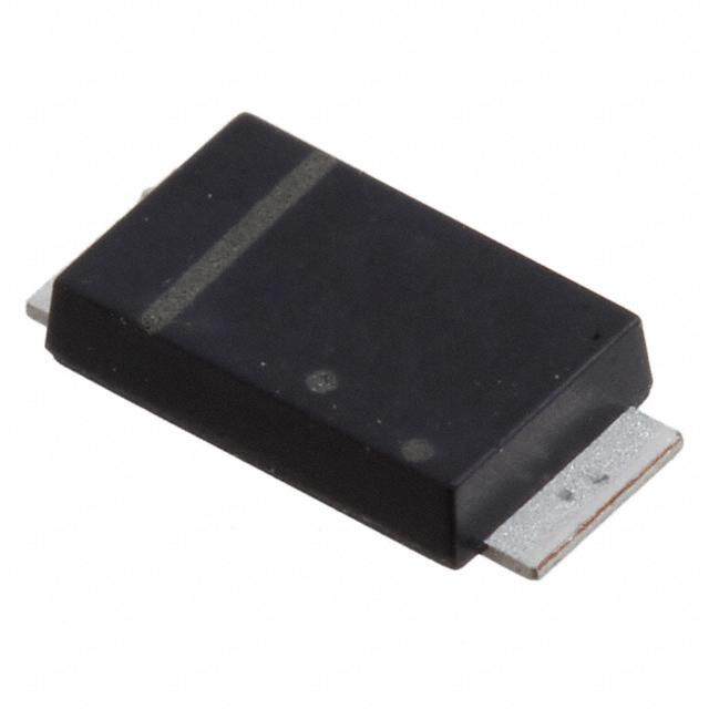
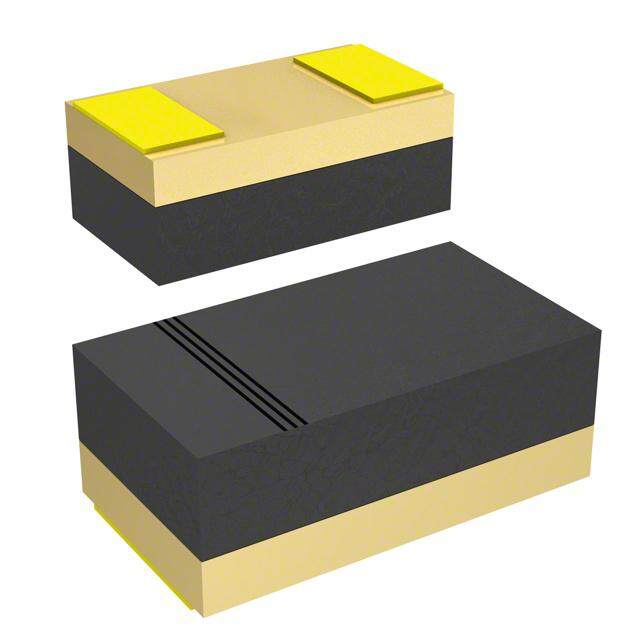
| 描述 | DIODE ZENER 20V 500MW SOD123稳压二极管 20V 500mW |
| 产品分类 | 单二极管/齐纳分离式半导体 |
| 品牌 | ON Semiconductor |
| 产品手册 | |
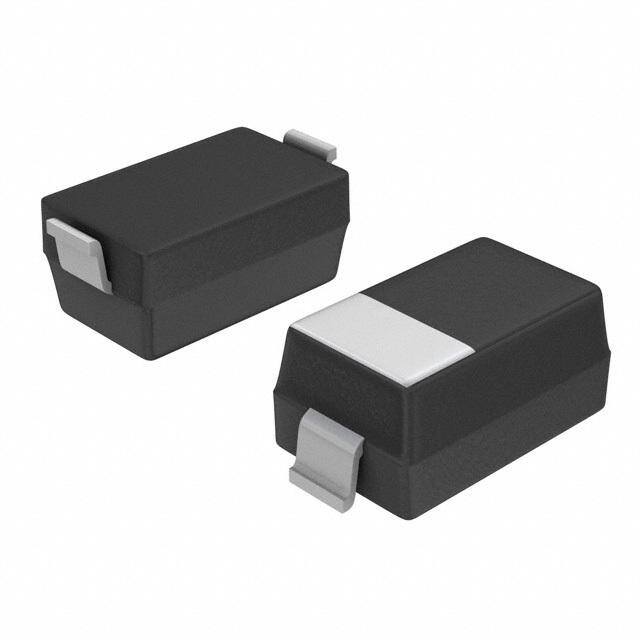
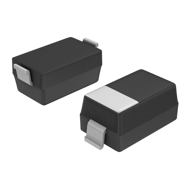
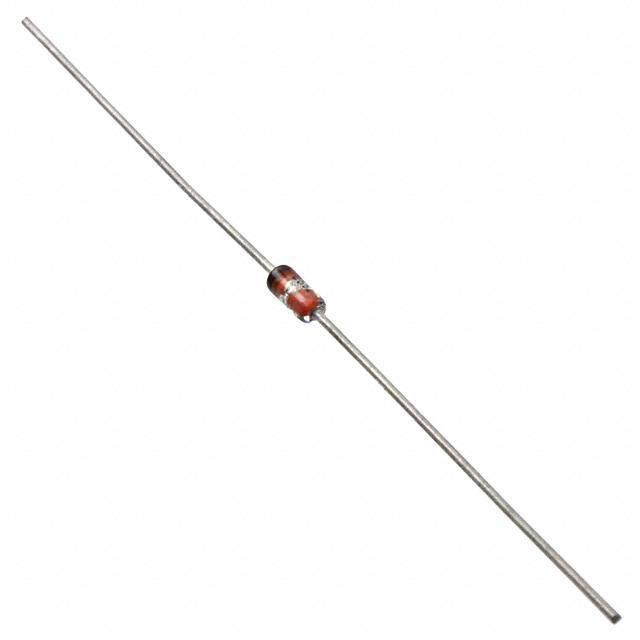
| 产品图片 |
|
| rohs | 符合RoHS无铅 / 符合限制有害物质指令(RoHS)规范要求 |
| 产品系列 | 二极管与整流器,稳压二极管,ON Semiconductor MMSZ4707T1G- |
| 数据手册 | |
| 产品型号 | MMSZ4707T1G |
| PCN组件/产地 | |
| PCN设计/规格 | |
| 不同If时的电压-正向(Vf) | 900mV @ 10mA |
| 不同 Vr时的电流-反向漏电流 | 10nA @ 15.2V |
| 产品种类 | Diodes- Zener |
| 供应商器件封装 | SOD-123 |
| 其它名称 | MMSZ4707T1GOSCT |
| 功率-最大值 | 500mW |
| 功率耗散 | 500 mW |
| 包装 | 剪切带 (CT) |
| 商标 | ON Semiconductor |
| 安装类型 | 表面贴装 |
| 安装风格 | SMD/SMT |
| 容差 | ±5% |
| 封装 | Reel |
| 封装/外壳 | SOD-123 |
| 封装/箱体 | SOD-123 |
| 工作温度 | -55°C ~ 150°C |
| 工厂包装数量 | 3000 |
| 最大反向漏泄电流 | 10 nA |
| 最大工作温度 | + 150 C |
| 最小工作温度 | - 55 C |
| 标准包装 | 1 |
| 电压-齐纳(标称值)(Vz) | 20V |
| 电压容差 | 3 % |
| 系列 | MMSZ4707 |
| 配置 | Single |
| 阻抗(最大值)(Zzt) | - |
| 齐纳电压 | 20 V |
| 齐纳电流 | 50 uA |


PDF Datasheet 数据手册内容提取
MMSZ4xxxT1G Series, SZMMSZ4xxxT1G Series Zener Voltage Regulators 500 mW, Low I SOD−123 Surface Mount ZT Three complete series of Zener diodes are offered in the convenient, www.onsemi.com surface mount plastic SOD−123 package. These devices provide a convenient alternative to the leadless 34−package style. Features • 500 mW Rating on FR−4 or FR−5 Board • Wide Zener Reverse Voltage Range − 1.8 V to 43 V • Low Reverse Current (IZT) − 50 (cid:2)A SOD−123 • Package Designed for Optimal Automated Board Assembly CASE 425 • STYLE 1 Small Package Size for High Density Applications • ESD Rating of Class 3 (>16 kV) per Human Body Model • SZ Prefix for Automotive and Other Applications Requiring Unique 1 2 Site and Control Change Requirements; AEC−Q101 Qualified and Cathode Anode PPAP Capable • These Devices are Pb−Free and are RoHS Compliant* MARKING DIAGRAM Mechanical Characteristics: CASE: Void-free, transfer-molded, thermosetting plastic case FINISH: Corrosion resistant finish, easily solderable 1 xxM(cid:2) (cid:2) MAXIMUM CASE TEMPERATURE FOR SOLDERING PURPOSES: 260°C for 10 Seconds POLARITY: Cathode indicated by polarity band xx = Device Code (Refer to page 3) FLAMMABILITY RATING: UL 94 V−0 M = Date Code (cid:2) = Pb−Free Package (Note: Microdot may be in either location) MAXIMUM RATINGS Rating Symbol Max Units ORDERING INFORMATION Total Power Dissipation on FR−5 Board, PD Device Package Shipping† (Note 1) @ TL = 75°C 500 mW Derated above 75°C 6.7 mW/°C MMSZ4xxxT1G SOD−123 3,000 / Thermal Resistance, (Note 2) R(cid:3)JA °C/W (Pb−Free) Tape & Reel Junction−to−Ambient 340 SZMMSZ4xxxT1G SOD−123 3,000 / (Pb−Free) Tape & Reel Thermal Resistance, (Note 2) R(cid:3)JL °C/W Junction−to−Lead 150 MMSZ4xxxT3G SOD−123 10,000 / (Pb−Free) Tape & Reel Junction and Storage Temperature Range TJ, Tstg −55 to °C +150 SZMMSZ4xxxT3G SOD−123 10,000 / (Pb−Free) Tape & Reel Stresses exceeding those listed in the Maximum Ratings table may damage the device. If any of these limits are exceeded, device functionality should not be †For information on tape and reel specifications, assumed, damage may occur and reliability may be affected. including part orientation and tape sizes, please 1. FR−5 = 3.5 X 1.5 inches, using the minimum recommended footprint. refer to our Tape and Reel Packaging Specifications 2. Thermal Resistance measurement obtained via infrared Scan Method. Brochure, BRD8011/D. DEVICE MARKING INFORMATION See specific marking information in the device marking column of the Electrical Characteristics table on page 3 of *For additional information on our Pb−Free strategy and soldering details, please this data sheet. download the ON Semiconductor Soldering and Mounting Techniques Reference Manual, SOLDERRM/D. © Semiconductor Components Industries, LLC, 2013 1 Publication Order Number: April, 2018 − Rev. 12 MMSZ4678T1/D
MMSZ4xxxT1G Series, SZMMSZ4xxxT1G Series ELECTRICAL CHARACTERISTICS (TA = 25°C unless I otherwise noted, VF = 0.9 V Max. @ IF = 10 mA) IF Symbol Parameter VZ Reverse Zener Voltage @ IZT IZT Reverse Current IR Reverse Leakage Current @ VR VZ VR V VR Reverse Voltage IIRZTVF IF Forward Current VF Forward Voltage @ IF Product parametric performance is indicated in the Electrical Characteristics for the listed test conditions, unless otherwise noted. Product performance may not be indicated by the Electrical Characteristics if operated under different conditions. Zener Voltage Regulator www.onsemi.com 2
MMSZ4xxxT1G Series, SZMMSZ4xxxT1G Series ELECTRICAL CHARACTERISTICS (TA = 25°C unless otherwise noted, VF = 0.9 V Max. @ IF = 10 mA) Zener Voltage (Note 3) Leakage Current Device VZ (Volts) @ IZT IR @ VR Device* Marking Min Nom Max (cid:2)A (cid:2)A Volts MMSZ4678T1G CC 1.71 1.8 1.89 50 7.5 1 MMSZ4679T1G CD 1.90 2.0 2.10 50 5 1 MMSZ4680T1G CE 2.09 2.2 2.31 50 4 1 MMSZ4681T1G CF 2.28 2.4 2.52 50 2 1 MMSZ4682T1G CH 2.565 2.7 2.835 50 1 1 MMSZ4683T1G CJ 2.85 3.0 3.15 50 0.8 1 MMSZ4684T1G CK 3.13 3.3 3.47 50 7.5 1.5 MMSZ4685T1G CM 3.42 3.6 3.78 50 7.5 2 MMSZ4686T1G CN 3.70 3.9 4.10 50 5 2 MMSZ4687T1G CP 4.09 4.3 4.52 50 4 2 SZMMSZ4687T1G CG6 4.09 4.3 4.52 50 4 2 MMSZ4688T1G CT 4.47 4.7 4.94 50 10 3 MMSZ4689T1G CU 4.85 5.1 5.36 50 10 3 MMSZ4690T1G/T3G CV 5.32 5.6 5.88 50 10 4 MMSZ4691T1G CA 5.89 6.2 6.51 50 10 5 MMSZ4692T1G CX 6.46 6.8 7.14 50 10 5.1 MMSZ4693T1G CY 7.13 7.5 7.88 50 10 5.7 MMSZ4694T1G CZ 7.79 8.2 8.61 50 1 6.2 MMSZ4695T1G DC 8.27 8.7 9.14 50 1 6.6 MMSZ4696T1G DD 8.65 9.1 9.56 50 1 6.9 MMSZ4697T1G DE 9.50 10 10.50 50 1 7.6 MMSZ4698T1G DF 10.45 11 11.55 50 0.05 8.4 MMSZ4699T1G DH 11.40 12 12.60 50 0.05 9.1 MMSZ4700T1G DJ 12.35 13 13.65 50 0.05 9.8 MMSZ4701T1G DK 13.30 14 14.70 50 0.05 10.6 MMSZ4702T1G DM 14.25 15 15.75 50 0.05 11.4 MMSZ4703T1G† DN 15.20 16 16.80 50 0.05 12.1 MMSZ4704T1G DP 16.15 17 17.85 50 0.05 12.9 MMSZ4705T1G DT 17.10 18 18.90 50 0.05 13.6 MMSZ4706T1G DU 18.05 19 19.95 50 0.05 14.4 MMSZ4707T1G DV 19.00 20 21.00 50 0.01 15.2 MMSZ4708T1G DA 20.90 22 23.10 50 0.01 16.7 MMSZ4709T1G DX 22.80 24 25.20 50 0.01 18.2 MMSZ4710T1G DY 23.75 25 26.25 50 0.01 19.0 MMSZ4711T1G† EA 25.65 27 28.35 50 0.01 20.4 MMSZ4712T1G EC 26.60 28 29.40 50 0.01 21.2 MMSZ4713T1G ED 28.50 30 31.50 50 0.01 22.8 MMSZ4714T1G EE 31.35 33 34.65 50 0.01 25.0 MMSZ4715T1G EF 34.20 36 37.80 50 0.01 27.3 MMSZ4716T1G EH 37.05 39 40.95 50 0.01 29.6 MMSZ4717T1G EJ 40.85 43 45.15 50 0.01 32.6 3. Nominal Zener voltage is measured with the device junction in thermal equilibrium at TL = 30°C ±1°C. *Include SZ-prefix devices where applicable. †MMSZ4703 and MMSZ4711 Not Available in 10,000/Tape & Reel www.onsemi.com 3
MMSZ4xxxT1G Series, SZMMSZ4xxxT1G Series TYPICAL CHARACTERISTICS 8 100 C) C) °V/ 7 °V/ TYPICAL TC VALUES m m T ( 6 TYPICAL TC VALUES T ( N N E 5 E CI CI FFI 4 VZ @ IZT FFI VZ @ IZT E E O 3 O E C E C 10 R 2 R U U AT 1 AT R R PE 0 PE M M E -1 E T T , Z , Z V -(cid:2)2 V θ θ -(cid:2)3 1 2 3 4 5 6 7 8 9 10 11 12 10 100 VZ, NOMINAL ZENER VOLTAGE (V) VZ, NOMINAL ZENER VOLTAGE (V) Figure 1. Temperature Coefficients Figure 2. Temperature Coefficients (Temperature Range −55°C to +150°C) (Temperature Range −55°C to +150°C) 1.2 1000 WATTS) 1.0 WATTS) RWEACVTEAFNOGRUML, ATRA = 25°C ON ( 0.8 PD versus TL WER ( 100 TI O A P DISSIP 0.6 PD versus TA SURGE R 0.4 AK 10 E E W P PO 0.2 P, pk , D P 0 1 0 25 50 75 100 125 150 0.1 1 10 100 1000 T, TEMPERATURE (5C) PW, PULSE WIDTH (ms) Figure 3. Steady State Power Derating Figure 4. Maximum Nonrepetitive Surge Power 1000 TJ = 25°C ΩE () IZ = 1 mA IfZ =(A 1C )k =H z0.1 IZ(DC) C AN 100 ED 5 mA P M C I MI 20 mA A YN 10 D , T Z Z 1 1 10 100 VZ, NOMINAL ZENER VOLTAGE Figure 5. Effect of Zener Voltage on Zener Impedance www.onsemi.com 4
MMSZ4xxxT1G Series, SZMMSZ4xxxT1G Series TYPICAL CHARACTERISTICS 1000 1000 TA = 25°C A) 0 V BIAS μ 100 1 V BIAS NT ( E 10 E (pF) 100 CURR 1 CAPACITANC 10 B50IA%S OAFT VZ NOM , LEAKAGE R00.0.11 +150°C C, I0.001 +(cid:2)25°C -(cid:2)55°C 0.0001 1 0.00001 1 10 100 0 10 20 30 40 50 60 70 80 90 VZ, NOMINAL ZENER VOLTAGE (V) VZ, NOMINAL ZENER VOLTAGE (V) Figure 6. Typical Capacitance Figure 7. Typical Leakage Current 100 100 TA = 25°C TA = 25°C mA) 10 mA) 10 T ( T ( N N E E R R R R U 1 U 1 C C R R E E N N E E Z Z , Z 0.1 , Z0.1 I I 0.01 0.01 0 2 4 6 8 10 12 10 30 50 70 90 VZ, ZENER VOLTAGE (V) VZ, ZENER VOLTAGE (V) Figure 8. Zener Voltage versus Zener Current Figure 9. Zener Voltage versus Zener Current (V Up to 12 V) (12 V to 91 V) Z www.onsemi.com 5
MECHANICAL CASE OUTLINE PACKAGE DIMENSIONS SOD−123 CASE 425−04 ISSUE G DATE 07 OCT 2009 SCALE 5:1 D A NOTES: 1.DIMENSIONING AND TOLERANCING PER ANSI A1 Y14.5M, 1982. ÂÂ1ÂÂ 2.CONTROLLING DIMENSION: INCH. MILLIMETERS INCHES ÂÂÂÂ DIM MIN NOM MAX MIN NOM MAX A 0.94 1.17 1.35 0.037 0.046 0.053 ÂÂÂÂ A1 0.00 0.05 0.10 0.000 0.002 0.004 b 0.51 0.61 0.71 0.020 0.024 0.028 HE E c --- --- 0.15 --- --- 0.006 D 1.40 1.60 1.80 0.055 0.063 0.071 E 2.54 2.69 2.84 0.100 0.106 0.112 HE 3.56 3.68 3.86 0.140 0.145 0.152 L 0.25 --- --- 0.010 --- --- (cid:2) 0° --- 10° 0° --- 10° 2 (cid:2) GENERIC b L MARKING DIAGRAM* C XXXM(cid:2) 1 SOLDERING FOOTPRINT* (cid:2) 0.91 XXX = Specific Device Code 0.036 ÉÉÉ ÉÉÉ M = Date Code (cid:2) = Pb−Free Package ÉÉÉ ÉÉÉ 1.22 (Note: Microdot may be in either location) 0.048 ÉÉÉ ÉÉÉ *This information is generic. Please refer to device data sheet for actual part marking. Pb−Free indicator, “G” or 2.36 microdot “ (cid:2)”, may or may not be present. 0.093 4.19 STYLE 1: 0.165 PIN 1. CATHODE 2. ANODE (cid:2) (cid:3) mm SCALE 10:1 inches *For additional information on our Pb−Free strategy and soldering details, please download the ON Semiconductor Soldering and Mounting Techniques Reference Manual, SOLDERRM/D. Electronic versions are uncontrolled except when accessed directly from the Document Repository. DOCUMENT NUMBER: 98ASB42927B Printed versions are uncontrolled except when stamped “CONTROLLED COPY” in red. DESCRIPTION: SOD−123 PAGE 1 OF 1 ON Semiconductor and are trademarks of Semiconductor Components Industries, LLC dba ON Semiconductor or its subsidiaries in the United States and/or other countries. ON Semiconductor reserves the right to make changes without further notice to any products herein. ON Semiconductor makes no warranty, representation or guarantee regarding the suitability of its products for any particular purpose, nor does ON Semiconductor assume any liability arising out of the application or use of any product or circuit, and specifically disclaims any and all liability, including without limitation special, consequential or incidental damages. ON Semiconductor does not convey any license under its patent rights nor the rights of others. © Semiconductor Components Industries, LLC, 2019 www.onsemi.com
ON Semiconductor and are trademarks of Semiconductor Components Industries, LLC dba ON Semiconductor or its subsidiaries in the United States and/or other countries. ON Semiconductor owns the rights to a number of patents, trademarks, copyrights, trade secrets, and other intellectual property. A listing of ON Semiconductor’s product/patent coverage may be accessed at www.onsemi.com/site/pdf/Patent−Marking.pdf. ON Semiconductor reserves the right to make changes without further notice to any products herein. ON Semiconductor makes no warranty, representation or guarantee regarding the suitability of its products for any particular purpose, nor does ON Semiconductor assume any liability arising out of the application or use of any product or circuit, and specifically disclaims any and all liability, including without limitation special, consequential or incidental damages. Buyer is responsible for its products and applications using ON Semiconductor products, including compliance with all laws, regulations and safety requirements or standards, regardless of any support or applications information provided by ON Semiconductor. “Typical” parameters which may be provided in ON Semiconductor data sheets and/or specifications can and do vary in different applications and actual performance may vary over time. All operating parameters, including “Typicals” must be validated for each customer application by customer’s technical experts. ON Semiconductor does not convey any license under its patent rights nor the rights of others. ON Semiconductor products are not designed, intended, or authorized for use as a critical component in life support systems or any FDA Class 3 medical devices or medical devices with a same or similar classification in a foreign jurisdiction or any devices intended for implantation in the human body. Should Buyer purchase or use ON Semiconductor products for any such unintended or unauthorized application, Buyer shall indemnify and hold ON Semiconductor and its officers, employees, subsidiaries, affiliates, and distributors harmless against all claims, costs, damages, and expenses, and reasonable attorney fees arising out of, directly or indirectly, any claim of personal injury or death associated with such unintended or unauthorized use, even if such claim alleges that ON Semiconductor was negligent regarding the design or manufacture of the part. ON Semiconductor is an Equal Opportunity/Affirmative Action Employer. This literature is subject to all applicable copyright laws and is not for resale in any manner. PUBLICATION ORDERING INFORMATION LITERATURE FULFILLMENT: TECHNICAL SUPPORT Email Requests to: orderlit@onsemi.com North American Technical Support: Europe, Middle East and Africa Technical Support: Voice Mail: 1 800−282−9855 Toll Free USA/Canada Phone: 00421 33 790 2910 ON Semiconductor Website: www.onsemi.com Phone: 011 421 33 790 2910 For additional information, please contact your local Sales Representative ◊ www.onsemi.com 1
Mouser Electronics Authorized Distributor Click to View Pricing, Inventory, Delivery & Lifecycle Information: O N Semiconductor: MMSZ4678T1G MMSZ4679T1G MMSZ4680T1G MMSZ4681T1G MMSZ4682T1G MMSZ4683T1G MMSZ4684T1G MMSZ4685T1G MMSZ4686T1G MMSZ4687T1G MMSZ4688T1G MMSZ4689T1G MMSZ4689T3G MMSZ4690T1G MMSZ4690T3G MMSZ4691T1G MMSZ4692T1G MMSZ4693T1G MMSZ4694T1G MMSZ4696T1G MMSZ4697T1G MMSZ4698T1G MMSZ4699T1G MMSZ4700T1G MMSZ4702T1G MMSZ4703T1G MMSZ4704T1G MMSZ4705T1G MMSZ4706T1G MMSZ4707T1G MMSZ4708T1G MMSZ4710T1G MMSZ4711T1G MMSZ4713T1G MMSZ4715T1G MMSZ4717T1G SZMMSZ4683T1G SZMMSZ4688T1G SZMMSZ4694T1G SZMMSZ4697T1G SZMMSZ4699T1G MMSZ4694T3G MMSZ4688T3G SZMMSZ4680T1G SZMMSZ4693T3G SMSZ4688ST1G SZMMSZ4717T1G SZMMSZ4700T1G SZMMSZ4708T1G SZMMSZ4694T3G SZMMSZ4688T3G SZMMSZ4687T1G SZMMSZ4698T1G