ICGOO在线商城 > 隔离器 > 光隔离器 - 逻辑输出 > MID400

 Datasheet下载
- 型号: MID400
- 制造商: Fairchild Semiconductor
- 库位|库存: xxxx|xxxx
- 要求:
| 数量阶梯 | 香港交货 | 国内含税 |
| +xxxx | $xxxx | ¥xxxx |
查看当月历史价格
查看今年历史价格
MID400产品简介:
ICGOO电子元器件商城为您提供MID400由Fairchild Semiconductor设计生产,在icgoo商城现货销售,并且可以通过原厂、代理商等渠道进行代购。 MID400价格参考。Fairchild SemiconductorMID400封装/规格:光隔离器 - 逻辑输出, Logic Output Optoisolator Open Collector 2500Vrms 1 Channel 8-DIP。您可以下载MID400参考资料、Datasheet数据手册功能说明书,资料中有MID400 详细功能的应用电路图电压和使用方法及教程。
ON Semiconductor的MID400光隔离器(逻辑输出)是一款广泛应用于工业和通信领域的器件,主要用于在电气系统中提供信号隔离。它通过光电转换技术,在输入端接收电信号并将其转换为光信号,再通过光耦合传输到输出端,重新转换为电信号,从而实现电气隔离,有效防止噪声干扰和电位差对电路的影响。

 应用场景:

1. 工业自动化:
   - MID400常用于工业控制系统中的信号传输,特别是在PLC(可编程逻辑控制器)、DCS(分布式控制系统)等设备中。它能够隔离不同电压等级的电路,确保系统的稳定性和安全性。

2. 电力系统:
   - 在电力监控、保护装置和智能电表中,MID400用于隔离高压侧和低压侧的信号,防止高电压对低压控制电路的损坏,同时确保数据的准确传输。

3. 通信设备:
   - 在通信基站、路由器、交换机等网络设备中,MID400用于隔离不同模块之间的信号,防止电磁干扰和地线噪声的影响,确保通信链路的可靠性。

4. 医疗设备:
   - 在医疗电子设备如心电图仪、监护仪等中,MID400用于隔离患者与设备之间的信号,确保患者的电气安全,同时提高设备的抗干扰能力。

5. 汽车电子:
   - 在汽车电子控制系统中,MID400用于隔离传感器与控制单元之间的信号,尤其是在混合动力和电动汽车中,它可以有效隔离高压电池系统与低压控制系统,确保车辆的安全运行。

6. 智能家居:
   - 在智能家居系统中,MID400可用于隔离各种传感器与主控板之间的信号,防止外界干扰,确保系统的稳定性和响应速度。

7. 电机驱动:
   - 在电机驱动器中,MID400用于隔离控制信号和功率信号,防止大电流波动对控制电路的影响,确保电机的精确控制。

总之,MID400凭借其可靠的电气隔离性能和广泛的适用性,成为众多应用场景中不可或缺的关键元件。
| 参数 | 数值 |
| 产品目录 | |
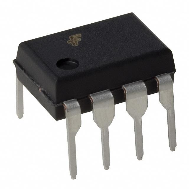
| 描述 | OPTOCOUPLER LOGIC-OUT 8-DIP逻辑输出光电耦合器 DIP-8 LOG OUT/AC IN |
| 产品分类 | |
| 品牌 | Fairchild Semiconductor |
| 产品手册 | |
| 产品图片 |
|
| rohs | 符合RoHS无铅 / 符合限制有害物质指令(RoHS)规范要求 |
| 产品系列 | 光耦合器/光电耦合器,逻辑输出光电耦合器,Fairchild Semiconductor MID400- |
| 数据手册 | |
| 产品型号 | MID400 |
| 上升/下降时间(典型值) | - |
| 上升时间 | 1 us |
| 下降时间 | 1 us |
| 产品目录页面 | |
| 产品种类 | 逻辑输出光电耦合器 |
| 传播延迟tpLH/tpHL(最大值) | 1ms, 1ms (标准) |
| 供应商器件封装 | 8-DIP |
| 共模瞬态抗扰度(最小值) | - |
| 其它名称 | MID400GI |
| 包装 | 管件 |
| 单位重量 | 819 mg |
| 商标 | Fairchild Semiconductor |
| 安装类型 | 通孔 |
| 封装 | Bulk |
| 封装/外壳 | 8-DIP(0.300",7.62mm) |
| 封装/箱体 | DIP-8 |
| 工作温度 | -40°C ~ 85°C |
| 工厂包装数量 | 1000 |
| 数据速率 | - |
| 最大功率耗散 | 115 mW |
| 最大工作温度 | + 85 C |
| 最大正向二极管电压 | 1.5 V |
| 最大正向二极管电流 | 30 mA |
| 最小工作温度 | - 40 C |
| 标准包装 | 1,000 |
| 每芯片的通道数量 | 1 Channel |
| 电压-正向(Vf)(典型值) | 1.5V (最小值) |
| 电压-电源 | 7V |
| 电压-隔离 | 2500Vrms |
| 电流-DC正向(If) | - |
| 电流-输出/通道 | 20mA |
| 系列 | MID400 |
| 绝缘电压 | 2500 Vrms |
| 输入-输入侧1/输入侧2 | 1/0 |
| 输入类型 | AC,DC |
| 输出类型 | Open Collector |
| 通道数 | 1 |
| 逻辑门类型 | AC Monitor-to-Logic |
| 零件号别名 | MID400_NL |


- 商务部:美国ITC正式对集成电路等产品启动337调查
- 曝三星4nm工艺存在良率问题 高通将骁龙8 Gen1或转产台积电
- 太阳诱电将投资9.5亿元在常州建新厂生产MLCC 预计2023年完工
- 英特尔发布欧洲新工厂建设计划 深化IDM 2.0 战略
- 台积电先进制程称霸业界 有大客户加持明年业绩稳了
- 达到5530亿美元!SIA预计今年全球半导体销售额将创下新高
- 英特尔拟将自动驾驶子公司Mobileye上市 估值或超500亿美元
- 三星加码芯片和SET,合并消费电子和移动部门,撤换高东真等 CEO
- 三星电子宣布重大人事变动 还合并消费电子和移动部门
- 海关总署:前11个月进口集成电路产品价值2.52万亿元 增长14.8%

PDF Datasheet 数据手册内容提取
Is Now Part of To learn more about ON Semiconductor, please visit our website at www.onsemi.com Please note: As part of the Fairchild Semiconductor integration, some of the Fairchild orderable part numbers will need to change in order to meet ON Semiconductor’s system requirements. Since the ON Semiconductor product management systems do not have the ability to manage part nomenclature that utilizes an underscore (_), the underscore (_) in the Fairchild part numbers will be changed to a dash (-). This document may contain device numbers with an underscore (_). Please check the ON Semiconductor website to verify the updated device numbers. The most current and up-to-date ordering information can be found at www.onsemi.com. Please email any questions regarding the system integration to Fairchild_questions@onsemi.com. ON Semiconductor and the ON Semiconductor logo are trademarks of Semiconductor Components Industries, LLC dba ON Semiconductor or its subsidiaries in the United States and/or other countries. ON Semiconductor owns the rights to a number of patents, trademarks, copyrights, trade secrets, and other intellectual property. A listing of ON Semiconductor’s product/patent coverage may be accessed at www.onsemi.com/site/pdf/Patent-Marking.pdf. ON Semiconductor reserves the right to make changes without further notice to any products herein. ON Semiconductor makes no warranty, representation or guarantee regarding the suitability of its products for any particular purpose, nor does ON Semiconductor assume any liability arising out of the application or use of any product or circuit, and specifically disclaims any and all liability, including without limitation special, consequential or incidental damages. Buyer is responsible for its products and applications using ON Semiconductor products, including compliance with all laws, regulations and safety requirements or standards, regardless of any support or applications information provided by ON Semiconductor. “Typical” parameters which may be provided in ON Semiconductor data sheets and/or specifications can and do vary in different applications and actual performance may vary over time. All operating parameters, including “Typicals” must be validated for each customer application by customer’s technical experts. ON Semiconductor does not convey any license under its patent rights nor the rights of others. ON Semiconductor products are not designed, intended, or authorized for use as a critical component in life support systems or any FDA Class 3 medical devices or medical devices with a same or similar classification in a foreign jurisdiction or any devices intended for implantation in the human body. Should Buyer purchase or use ON Semiconductor products for any such unintended or unauthorized application, Buyer shall indemnify and hold ON Semiconductor and its officers, employees, subsidiaries, affiliates, and distributors harmless against all claims, costs, damages, and expenses, and reasonable attorney fees arising out of, directly or indirectly, any claim of personal injury or death associated with such unintended or unauthorized use, even if such claim alleges that ON Semiconductor was negligent regarding the design or manufacture of the part. ON Semiconductor is an Equal Opportunity/Affirmative Action Employer. This literature is subject to all applicable copyright laws and is not for resale in any manner.
M I D 4 September 2016 0 0 A C L MID400 in e AC Line Monitor Logic-Out Device M o n i t o Features Description r L o • Direct operation from any line voltage with the use of The MID400 is an optically isolated AC line-to-logic inter- g an external resistor. face device. It is packaged in an 8-lead plastic DIP. The ic • Externally adjustable time delay AC line voltage is monitored by two back-to-back GaAs -O • Externally adjustable AC voltage sensing level LED diodes in series with an external resistor. A high u • Logic level compatibility gain detector circuit senses the LED current and drives t D • Safety and Regulatory Approvals: the output gate to a logic low condition. e v – UL1577, 2,500 VACRMS for 1 Minute The MID400 has been designed solely for the use as an ic – DIN-EN/IEC60747-5-5, 630 V Peak Working AC line monitor. It is recommended for use in any AC-to- e Insulation Voltage DC control application where excellent optical iso- lation, solid state reliability, TTL compatibility, small size, low power, and low frequency operations are required. Applications • Monitoring of the AC/DC “line-down” condition • “Closed-loop” interface between electromechanical elements such as solenoids, relay contacts, small motors, and microprocessors • Time delay isolation switch Functional Schematic Package Outlines 1 8 (cid:57)(cid:38)(cid:38) 8 (cid:49)(cid:18)(cid:38) 2 7 (cid:36)(cid:56)(cid:59) 1 3 6 (cid:57) (cid:50) 8 8 (cid:49)(cid:18)(cid:38) 4 5 (cid:42)(cid:49)(cid:39) 1 1 Figure 1. Schematic Figure 2. Package Outlines ©2005 Fairchild Semiconductor Corporation www.fairchildsemi.com MID400 AC Line Monitor Logic-Out Device Rev. 1.1 1
M I Safety and Insulation Ratings D 4 0 As per DIN EN/IEC 60747-5-5, this optocoupler is suitable for “safe electrical insulation” only within the safety limit 0 data. Compliance with the safety ratings shall be ensured by means of protective circuits. A C Parameter Characteristics L i Installation Classifications per DIN VDE < 150 VRMS I–IV ne 0110/1.89 Table 1, For Rated Mains Voltage < 300 VRMS I–IV M Climatic Classification 55/100/21 o n Pollution Degree (DIN VDE 0110/1.89) 2 it o Comparative Tracking Index 175 r L o g i c Symbol Parameter Value Unit - O Input-to-Output Test Voltage, Method A, V x 1.6 = V , u IORM PR 1008 V t Type and Sample Test with tm = 10 s, Partial Discharge < 5 pC peak D V PR Input-to-Output Test Voltage, Method B, V x 1.875 = V , e IORM PR 1182 V v 100% Production Test with tm = 1 s, Partial Discharge < 5 pC peak ic e V Maximum Working Insulation Voltage 630 V IORM peak V Highest Allowable Over-Voltage 6000 V IOTM peak External Creepage 7 mm External Clearance 7 mm DTI Distance Through Insulation (Insulation Thickness) 0.4 mm T Case Temperature(1) 150 °C S I Input Current(1) 60 mA S,INPUT P Output Power(1) 150 mW S,OUTPUT R Insulation Resistance at T , V = 500 V(1) > 109 IO S IO Note: 1. Safety limit values – maximum values allowed in the event of a failure. ©2005 Fairchild Semiconductor Corporation www.fairchildsemi.com MID400 AC Line Monitor Logic-Out Device Rev. 1.1 2
M I Absolute Maximum Ratings D 4 0 Stresses exceeding the absolute maximum ratings may damage the device. The device may not function or be opera- 0 ble above the recommended operating conditions and stressing the parts to these levels is not recommended. In addi- A tion, extended exposure to stresses above the recommended operating conditions may affect device reliability. The C absolute maximum ratings are stress ratings only. L i n e M Symbol Parameter Value Unit o n T Storage Temperature -55 to +125 °C STG i t T Operating Temperature -40 to +85 °C o OPR r T Junction Temperature -55 to +100 °C L J o T Lead Solder Temperature 260 for 10 seconds °C g SOL i c Total Device Power Dissipation @ TA = 25°C 115 mW - P O D Derate Above 70°C 4 mW/°C u t EMITTER D e RMS Current 25 mA v i DC Current ±30 mA c e LED Power Dissipation @ T = 25°C 45 mW A P D(EMITTER) Derate Above 70°C 2 mW/°C DETECTOR I Low Level Output Current 20 mA OL V High Level Output Voltage 7 V OH V Supply Voltage 7 V CC Detector Power Dissipation @ T = 25°C 70 mW A P D(DETECTOR) Derate Above 70°C 2 mW/°C ©2005 Fairchild Semiconductor Corporation www.fairchildsemi.com MID400 AC Line Monitor Logic-Out Device Rev. 1.1 3
M I Electrical Characteristics D 4 0°C to 70°C Free Air Temperature unless otherwise specified. 0 0 Individual Component Characteristics A C Symbol Parameter Test Conditions Min. Typ. Max. Unit L EMITTER in e V Input Forward Voltage I = ±30 mA 1.5 V F IN(DC) M DETECTOR o n IIN(RMS) = 4.0 mA, ito ICCL Logic Low Output Supply Current VO = Open, VCC = 5.5V, 3.0 mA r 24 V ≤ VIN(ON_RMS) ≤ 240 V L o IIN(RMS) = 0.15 mA, g ICCH Logic High Output Supply Current VCC = 5.5 V, 0.8 mA ic V ≥ 5.5 V - IN(OFF_RMS) O u t D Transfer Characteristics e v i c Symbol Parameter Test Conditions Min. Typ. Max. Unit e DC CHARACTERISTICS I = I , I = 16 mA, IN IN(ON_RMS) O V Logic Low Output Current V = 4.5 V, 0.18 0.40 V OL CC 24 V ≤ V ≤ 240 V IN(ON_RMS) I = 0.15 mA, IN(RMS) I Logic High Output Current V = V = 5.5 V, 0.02 100 µA OH O CC V ≥ 5.5 V IN(OFF_RMS) I = 16 mA, O V On-state RMS Input Voltage V = 0.4 V, V = 4.5 V, 90 V IN(ON_RMS) O CC R = 22 kΩ IN I ≤ 100 µA, O V Off-state RMS Input Voltage V = V = 5.5 V, 5.5 V IN(OFF_RMS) O CC R = 22 kΩ IN I = 16 mA, O I On-state RMS Input Current V = 0.4 V, V = 4.5 V, 4.0 mA IN(ON_RMS) O CC 24 V ≤ V ≤ 240 V IN(ON_RMS) I ≤ 100 µA, O I Off-state RMS Input Current V = V = 5.5 V, 0.15 mA IN(OFF_RMS) O CC V ≥ 5.5 V IN(OFF_RMS) AC CHARACTERISTICS tON Turn-On Time IIN(RMS) = 4.0 mA, IO = 16 mA, 1.0 ms V = 4.5 V, R = 22 kΩ CC IN tOFF Turn-Off Time (See figure 4) 1.0 ms Isolation Characteristics Symbol Parameter Test Conditions Min. Typ. Max. Unit Relative Humidity ≤ 50%, V Steady State Isolation Voltage 2,500 VAC ISO I ≤ 10 µA, 1 Minute, 60 Hz RMS I-O C Isolation Capacitance f = 1 MHz 2 pF ISO R Isolation Resistance V = 500 VDC 1011 Ω ISO I-O ©2005 Fairchild Semiconductor Corporation www.fairchildsemi.com MID400 AC Line Monitor Logic-Out Device Rev. 1.1 4
M I D 4 0 (cid:36)pplications(cid:3)(cid:44)(cid:81)(cid:73)(cid:82)(cid:85)(cid:80)(cid:68)(cid:87)(cid:76)(cid:82)(cid:81) Glossary 0 A The input of the MID400 consists of two back-to-back(cid:3) VOLTAGES C LED diodes which will accept and convert alternating(cid:3) V On-State RMS Input Voltage L currents into light energy. An integrated photo diode- I(cid:49) (ON(cid:66)(cid:53)(cid:48)(cid:54)) i n detector amplifier forms the output network. Optical cou- The RMS voltage at an input terminal for a(cid:3) e pling between input and output provides 2500 V(cid:36)(cid:38)RMS(cid:3) specified input current with output condi- M voltage isolation. A very high current transfer ratio(cid:3) tions applied according to the product(cid:3) o (defined as the ratio of the DC output current and the DC(cid:3) specification will cause the output switch- n i input current) is achieved through the use of high gain(cid:3) ing element to be sustained in the on-state(cid:3) to amplifier. The detector amplifier circuitry operates from a(cid:3) within one full cycle. r 5V DC supply and drives an open collector transistor(cid:3) L V Off-State RMS Input Voltage o output. The switching times are intentionally designed to(cid:3) I(cid:49) (OFF(cid:66)(cid:53)(cid:48)(cid:54)) g be slow in order to enable the MID400, when used as an(cid:3) The RMS voltage at an input terminal for a(cid:3) ic AC line monitor, to respond only to changes in input volt- specified input current with output condi- -O age exceeding many milliseconds. The short period of(cid:3) tions applied according to the product(cid:3) u time during zero-crossing which occurs once every half(cid:3) specification will cause the output switch- t D cycle of the power line is completely ignored. To operate ing element to be sustained in the off-state(cid:3) e the MID400, always add a resistor, RIN, in series with within one full cycle. v i the(cid:3)input (as shown in (cid:73)(cid:76)(cid:74)(cid:88)(cid:85)(cid:72)(cid:3)(cid:22)) to limit the current to the(cid:3) c required value. The value of the resistor can be deter- VOL Low-Level Output Voltage e mined by the following equation: The voltage at an output terminal for a spe- cific output current I , with input condi- OL RIN = V-----I--N-I----–----V-----F-- stipoencsi ficaaptpioline dw iall cceosrtdaibnligs h toa tlohwe -lepvreold uact(cid:3)t(cid:3) IN the output. Where, V High-Level Output Voltage OH V (RMS) is the input voltage. IN The voltage at an output terminal for a spe- VF is the forward voltage drop across the LED. cific output current IOH, with input condi- IIN (RMS) is the desired input current required to sustain a logic tions applied according to the product(cid:3) “O” on the output. specification will establish a high-level at(cid:3) the output. Pin Description V LED Forward Voltage F Pin Pin The voltage developed across the LED Number Name Function when input current IF is applied to the(cid:3) 1, 3 V , V Input terminals anode of the LED. IN1 IN2 2, 4 N/C No Connect CURRENTS 8 VCC Supply voltage, output circuit. II(cid:49) (ON(cid:66)(cid:53)(cid:48)(cid:54)) On-State RMS Input Current 7 AUX Auxiliary terminal. The RMS current flowing into an input with(cid:3) Programmable capacitor input output conditions applied according to(cid:3)the to adjust AC voltage sensing product specification will cause the(cid:3)output level and time delay. switching element to be sustained(cid:3)in the 6 V Output terminal; open collector. on-state within one full cycle. O 5 GND Circuit ground potential. II(cid:49) (OFF(cid:66)(cid:53)(cid:48)(cid:54))(cid:3) Off-state RMS Input Current The RMS current flowing into an input with(cid:3) Schematic Diagram output conditions applied according to(cid:3)the product specification will cause the(cid:3)output switching element to be sustained(cid:3)in the VIN1 1 8 VCC off-state within one full cycle. I High-Level Output Current N/C 2 7 AUX. OH The current flowing into an output (cid:3)with VIN2 3 6 VO input conditions applied according t(cid:3)othe product specification will establish(cid:3) haigh- N/C 4 5 GND level at the output. ©2005 Fairchild Semiconductor Corporation www.fairchildsemi.com MID400 AC Line Monitor Logic-Out Device Rev. 1.1 5
M I D 4 0 0 A C IOL Low-Level Output Current DYNAMIC CHARACTERISTICS L The current flowing into an output (cid:3)with tON Turn-On Time in input conditions applied according t(cid:3)othe e The time between the specified reference product specification will establish(cid:3) loaw- M points on the input and the output voltage level at the output. o waveforms with the output changing from n ICCL Supply Current, Output LOW the defined high-level to the defined low- ito The current flowing into the VCC supply(cid:3) level. r L terminal of a circuit when the output is at a tOFF Turn-Off time o low-level voltage. g The time between the specified reference i c ICCH Supply Current, Output HIGH points on the input and the output voltage -O waveforms with the output changing from The current flowing into the VCC supply(cid:3) u terminal of a circuit when the output is at a the defined low-level to the defined high- t level. D high-level voltage. e v i c e ©2005 Fairchild Semiconductor Corporation www.fairchildsemi.com MID400 AC Line Monitor Logic-Out Device Rev. 1.1 6
M I D 4 (cid:55)(cid:72)(cid:86)(cid:87)(cid:3)(cid:38)(cid:76)(cid:85)(cid:70)(cid:88)(cid:76)(cid:87)(cid:86) 0 0 A VCC C L RIN = 22kΩ in 1 8 e M AC IVNINPUT 2 7 RL = 300Ω on i CAUX to r 3 6 VO L o g i c 4 5 - O u t D INPUT CURRENT VS. CAPACITANCE, CAUX CIRCUIT e v (cid:41)(cid:76)(cid:74)(cid:88)(cid:85)(cid:72)(cid:3)(cid:22)(cid:17)(cid:3)(cid:55)(cid:92)(cid:83)(cid:76)(cid:70)(cid:68)(cid:79)(cid:3)(cid:36)(cid:83)(cid:83)(cid:79)(cid:76)(cid:70)(cid:68)(cid:87)(cid:76)(cid:82)(cid:81)(cid:3)(cid:38)(cid:76)(cid:85)(cid:70)(cid:88)(cid:76)(cid:87) ic e A-C INPUT OV tON tOFF VOH OUTPUT 50% 50% VOL *INPUT TURNS ON AND OFF AT ZERO CROSSING +4.5V VCC 1 1 INPUT VCC 8 A-C 2 N/C AUX. 7 RL 300Ω INPUT RIN 3 2 INPUT VOUT 6 22kΩ OUTPUT 4 N/C GND 5 TEST CIRCUIT (cid:41)(cid:76)(cid:74)(cid:88)(cid:85)(cid:72)(cid:3)(cid:23)(cid:17)(cid:3)(cid:48)(cid:44)(cid:39)(cid:23)(cid:19)(cid:19)(cid:3)(cid:54)(cid:90)(cid:76)(cid:87)(cid:70)(cid:75)(cid:76)(cid:81)(cid:74)(cid:3)(cid:55)(cid:76)(cid:80)(cid:72) ©2005 Fairchild Semiconductor Corporation www.fairchildsemi.com MID400 AC Line Monitor Logic-Out Device Rev. 1.1 7
M I D 4 Typical Performance Curves 0 0 A C 250 30 L i VTAC C= =2 55°.C0V 25 VTAC C= =2 55°.C0V ne MS) 200 MS) Mo AC INPUT VOLTAGE (R 11505000 TURN ON AC INPUT VOLTAGE (R 1120505 TURN OFF IOH ≤ μA nitor Logic-O IOL = 16mA u t 0 0 D 0 10 20 30 40 50 60 0 10 20 30 40 50 60 e v INPUT RESITANCE, RIN (kV) INPUT RESITANCE, RIN (kΩ) ic Fig. (cid:24) Input Voltage vs. Input Resistance Fig. (cid:25) Input Voltage vs. Input Resistance e 120 2.8 2.4 S VCC = 5.0V LIZED (%) 110 T (mA) RM 12..60 IRITOOAILHN = =≤= 2 1μ256A2°mkCΩA MA 100 EN II(cid:49) (ON) NOR ICCL URR 1.2 I – CC 90 PUT C 0.8 II(cid:49) (OFF) ICCH IN 0.4 80 0 4.5 4.6 4.7 4.8 4.9 5.0 5.1 5.2 5.3 5.4 5.5 10 20 50 100 200 500 1000 VCC – SUPPLY VOLTAGE (V) CAPACITANCE (pF) (AUX. TO GND) Fig. (cid:26) Supply Current vs. Supply Voltage Fig. (cid:27) Input Current vs. Capacitance 0.30 4.5 V V) 5.0 V E ( 0.20 G TA II(cid:49) (ON(cid:66)(cid:53)(cid:48)(cid:54)) = 4.0 mA OL 0.15 V T U P T 0.10 U O – L O 0.05 V 0 0 5.0 10.0 15.0 20.0 25.0 IOL – OUTPUT CURRENT (mA) Fig. (cid:28) Output Voltage vs. Output Current ©2005 Fairchild Semiconductor Corporation www.fairchildsemi.com MID400 AC Line Monitor Logic-Out Device Rev. 1.1 8
M I Ordering Information D 4 0 Part Number Package Packing Method 0 A MID400 DIP 8-Pin Tube (50 units per tube) C MID400S SMT 8-Pin (Lead Bend) Tube (50 units per tube) L i n MID400SD SMT 8-Pin (Lead Bend) Tape and Reel (1,000 units per reel) e M MID400V DIP 8-Pin, DIN EN/IEC 60747-5-5 Option Tube (50 units per tube) o MID400SV SMT 8-Pin (Lead Bend), DIN EN/IEC 60747-5-5 Option Tube (50 units per tube) n i t MID400SDV SMT 8-Pin, DIN EN/IEC 60747-5-5 Option Tape and Reel (1,000 units per reel) o r MID400WV DIP 8-Pin, 0.4” Lead Spacing, DIN EN/IEC 60747-5-5 Tube (50 units per tube) L o Option g i c - O u t D e Marking Information v i c e 1 MID400 2 V XX YY T1 6 3 4 5 Figure 10. Top Mark Table 1. Top Mark Definitions 1 Fairchild Logo 2 Device Number 3 DIN EN/IEC60747-5-5 Option (only appears on component ordered with this option) 4 Two-Digit Year Code, e.g., “06” 5 Digit Work Week, Ranging from “01” to “53” 6 Assembly Package Code ©2005 Fairchild Semiconductor Corporation www.fairchildsemi.com MID400 AC Line Monitor Logic-Out Device Rev. 1.1 9
None
None
None
ON Semiconductor and are trademarks of Semiconductor Components Industries, LLC dba ON Semiconductor or its subsidiaries in the United States and/or other countries. ON Semiconductor owns the rights to a number of patents, trademarks, copyrights, trade secrets, and other intellectual property. A listing of ON Semiconductor’s product/patent coverage may be accessed at www.onsemi.com/site/pdf/Patent−Marking.pdf. ON Semiconductor reserves the right to make changes without further notice to any products herein. ON Semiconductor makes no warranty, representation or guarantee regarding the suitability of its products for any particular purpose, nor does ON Semiconductor assume any liability arising out of the application or use of any product or circuit, and specifically disclaims any and all liability, including without limitation special, consequential or incidental damages. Buyer is responsible for its products and applications using ON Semiconductor products, including compliance with all laws, regulations and safety requirements or standards, regardless of any support or applications information provided by ON Semiconductor. “Typical” parameters which may be provided in ON Semiconductor data sheets and/or specifications can and do vary in different applications and actual performance may vary over time. All operating parameters, including “Typicals” must be validated for each customer application by customer’s technical experts. ON Semiconductor does not convey any license under its patent rights nor the rights of others. ON Semiconductor products are not designed, intended, or authorized for use as a critical component in life support systems or any FDA Class 3 medical devices or medical devices with a same or similar classification in a foreign jurisdiction or any devices intended for implantation in the human body. Should Buyer purchase or use ON Semiconductor products for any such unintended or unauthorized application, Buyer shall indemnify and hold ON Semiconductor and its officers, employees, subsidiaries, affiliates, and distributors harmless against all claims, costs, damages, and expenses, and reasonable attorney fees arising out of, directly or indirectly, any claim of personal injury or death associated with such unintended or unauthorized use, even if such claim alleges that ON Semiconductor was negligent regarding the design or manufacture of the part. ON Semiconductor is an Equal Opportunity/Affirmative Action Employer. This literature is subject to all applicable copyright laws and is not for resale in any manner. PUBLICATION ORDERING INFORMATION LITERATURE FULFILLMENT: N. American Technical Support: 800−282−9855 Toll Free ON Semiconductor Website: www.onsemi.com Literature Distribution Center for ON Semiconductor USA/Canada 19521 E. 32nd Pkwy, Aurora, Colorado 80011 USA Europe, Middle East and Africa Technical Support: Order Literature: http://www.onsemi.com/orderlit Phone: 303−675−2175 or 800−344−3860 Toll Free USA/Canada Phone: 421 33 790 2910 Fax: 303−675−2176 or 800−344−3867 Toll Free USA/Canada Japan Customer Focus Center For additional information, please contact your local Email: orderlit@onsemi.com Phone: 81−3−5817−1050 Sales Representative © Semiconductor Components Industries, LLC www.onsemi.com www.onsemi.com 1
Mouser Electronics Authorized Distributor Click to View Pricing, Inventory, Delivery & Lifecycle Information: O N Semiconductor: MID400SV MID400SD MID400WV MID400SDV MID400V MID400S MID400