ICGOO在线商城 > 隔离器 > 光隔离器 - 逻辑输出 > TLP2631TP1F
 Datasheet下载
- 型号: TLP2631TP1F
- 制造商: Toshiba America Electronic Components, Inc.
- 库位|库存: xxxx|xxxx
- 要求:
| 数量阶梯 | 香港交货 | 国内含税 |
| +xxxx | $xxxx | ¥xxxx |
查看当月历史价格
查看今年历史价格
TLP2631TP1F产品简介:
ICGOO电子元器件商城为您提供TLP2631TP1F由Toshiba America Electronic Components, Inc.设计生产,在icgoo商城现货销售,并且可以通过原厂、代理商等渠道进行代购。 TLP2631TP1F价格参考。Toshiba America Electronic Components, Inc.TLP2631TP1F封装/规格:光隔离器 - 逻辑输出, Logic Output Optoisolator 10MBd Open Collector, Schottky Clamped 2500Vrms 2 Channel 1kV/µs CMTI 8-SMD。您可以下载TLP2631TP1F参考资料、Datasheet数据手册功能说明书,资料中有TLP2631TP1F 详细功能的应用电路图电压和使用方法及教程。
Toshiba Semiconductor and Storage(东芝半导体与存储)生产的TLP2631TP1F是一款光隔离器,属于逻辑输出类型。这种器件主要用于实现电气信号的光电隔离,以保护电路免受噪声、干扰或高压的影响。以下是其典型应用场景:

 1. 工业自动化控制
   - 在工业控制系统中,TLP2631TP1F可用于隔离输入/输出信号,防止强电干扰影响微控制器或其他低电压电路。
   - 应用于可编程逻辑控制器(PLC)、传感器接口和驱动电路中,确保信号传输的稳定性和安全性。

 2. 电机驱动与逆变器
   - 在电机驱动和逆变器系统中,该光隔离器可以将控制电路与功率级电路隔离开来,避免高电压对控制部分的损害。
   - 常见于变频器、伺服驱动器等设备中,用于隔离栅极驱动信号。

 3. 电源管理
   - TLP2631TP1F适用于开关电源(SMPS)和直流-直流转换器中的反馈信号隔离,确保初级侧和次级侧电路的安全性。
   - 在光伏逆变器中,也可用于隔离电网与内部电路之间的通信信号。

 4. 医疗设备
   - 在医疗电子设备中,如心电图机、超声波设备等,该光隔离器能够隔离患者接触部分与主电路之间的电气连接,保障患者和设备的安全。

 5. 通信与网络设备
   - 用于隔离数据通信中的输入/输出信号,例如在以太网供电(PoE)系统中,防止浪涌电流或高压对敏感电路的破坏。
   - 在远程监控系统中,提供可靠的信号隔离功能。

 6. 汽车电子
   - 在汽车电子控制系统中,如发动机控制单元(ECU)、车载充电器等,TLP2631TP1F可用于隔离高低电压域之间的信号,提高系统的可靠性和抗干扰能力。

 7. 家用电器
   - 在智能家电中,如空调、洗衣机等,该光隔离器可用于隔离用户界面与核心控制电路之间的信号,确保操作安全。

 总结
TLP2631TP1F凭借其高隔离电压、快速响应时间和稳定的性能,在需要电气隔离的各种场景中表现出色。它特别适合那些需要在恶劣环境下工作的应用,能够有效提升系统的可靠性和安全性。
| 参数 | 数值 |
| 品牌 | Toshiba |
| 产品目录 | 半导体 |
| 描述 | 高速光耦合器 IC cplr dual ch 10Mbps |
| 产品分类 | 集成电路 - IC |
| 产品手册 | |
| 产品图片 |
|
| rohs | 符合RoHS |
| 产品系列 | 光耦合器/光电耦合器,高速光耦合器,Toshiba TLP2631TP1F |
| 产品型号 | TLP2631TP1F |
| 上升时间 | 30 ns |
| 下降时间 | 30 ns |
| 产品种类 | 高速光耦合器 |
| 商标 | Toshiba |
| 封装 | Reel |
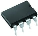
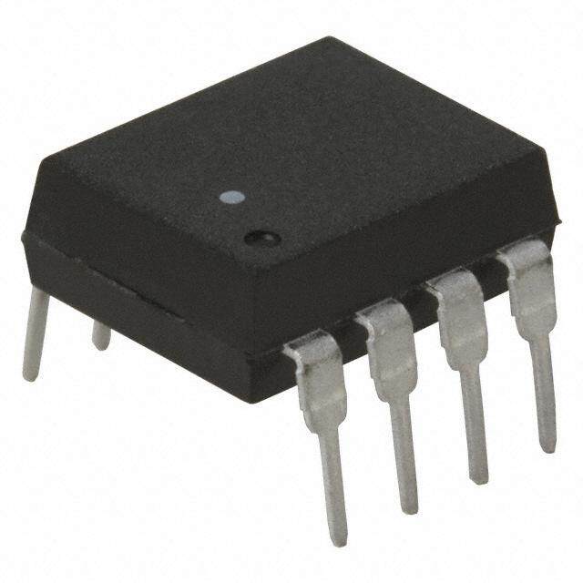
| 封装/箱体 | PDIP-8 |
| 工厂包装数量 | 1500 |
| 数据速率 | 10 MBd |
| 最大功率耗散 | 40 mW |
| 最大反向二极管电压 | 5 V |
| 最大工作温度 | + 85 C |
| 最大正向二极管电压 | 1.75 V |
| 最大正向二极管电流 | 20 mA |
| 最大连续输出电流 | 16 mA |
| 最小工作温度 | - 40 C |
| 最小正向二极管电压 | 1.75 V |
| 正向电流 | 20 mA |
| 每芯片的通道数量 | 2 Channels |
| 绝缘电压 | 2500 Vrms |
| 输出设备 | Photo IC |


- 商务部:美国ITC正式对集成电路等产品启动337调查
- 曝三星4nm工艺存在良率问题 高通将骁龙8 Gen1或转产台积电
- 太阳诱电将投资9.5亿元在常州建新厂生产MLCC 预计2023年完工
- 英特尔发布欧洲新工厂建设计划 深化IDM 2.0 战略
- 台积电先进制程称霸业界 有大客户加持明年业绩稳了
- 达到5530亿美元!SIA预计今年全球半导体销售额将创下新高
- 英特尔拟将自动驾驶子公司Mobileye上市 估值或超500亿美元
- 三星加码芯片和SET,合并消费电子和移动部门,撤换高东真等 CEO
- 三星电子宣布重大人事变动 还合并消费电子和移动部门
- 海关总署:前11个月进口集成电路产品价值2.52万亿元 增长14.8%


PDF Datasheet 数据手册内容提取
TLP2631 TOSHIBA photocoupler GaAℓAs IRed & Photo IC TLP2631 Isolated Line Receiver Simplex / Multiplex Data Transmission Computer-Peripheral Interface Microprocessor System Interface Unit: mm Digital Isolation for A / D, D / A Conversion The TOSHIBA TLP2631 dual photocoupler consists of a pair of GaAℓAs light emitting diode and integrated high gain, high speed photodetector. This unit is 8-lead DIP. The output of the detector circuit is an open collector, Schottky clamped transistor. A Faraday shield integrated on the photodetector chip reduces the effects of capacitive coupling between the input LED emitter and the high gain stages of the detector. This provides an effective common mode transient immunity of 1000 V/μs. • Input current threshold: IF = 5 mA (max) • Switching speed: 10MBd (typ.) • Common mode transient immunity: ±1000 V/μs (min) • Guaranteed performance over temperature: 0 to 70°C • Isolation voltage: 2500 Vrms (min) • UL recognized: UL1577, file no. E67349 TOSHIBA 11−10C4 • cUL approved :CSA Component Acceptance Service Weight: 0.54 g (typ.) No. 5A, File No.E67349 Truth Table (positive logic) Pin Configuration (top view) Input Output H L 1 VCC 8 1 : Anode 1 L H 2 : Cathode 1 3 : Cathode 2 2 7 4 : Anode 2 3 6 5 : GND Schematic 6 : VO2 (Output 2) GND 1 IF1 Shield ICC 8 4 Shield 5 78 :: VVOCC1 (Output 1) + VCC VF1 2 IO1 7 VO1 − IF2 IO2 4 6 + VO2 VF2 3 − 5 GND A 0.01 to 0.1μF bypass capacitor must be connected between pins 8 and 5(see Note 1). Start of commercial production 1986-03 1 2017-08-21
TLP2631 Absolute Maximum Ratings (no derating required up to 70°C) Characteristic Symbol Rating Unit Forward current (each channel) IF 20 mA Pulse forward current (each channel)* IFP 30 mA D Reverse voltage (each channel) VR 5 V E L Input power dissipation(each channel) PD 25 mW Input power dissipation derating (Ta ≥ 70°C) (each channel) ΔPD/°C -0.45 mW/°C Output current (each channel) IO 16 mA Output voltage (each channel) VO −0.5 to 7 V or Supply voltage VCC 7 V ct (1 minute maximum) e et D Output collector power PO 40 mW dissipation (each channel) Output power dissipation derating (Ta ≥ 70°C) (each channel) ΔPO/°C -0.75 mW/°C Storage temperature range Tstg −55 to 125 °C Operating temperature range Topr −40 to 85 °C Lead soldering temperature (10s)** Tsol 260 °C Isolation voltage BVS 2500 Vrms (AC, 1 minute, R.H.≤ 60%, Ta=25°C (Note 3) Note: Using continuously under heavy loads (e.g. the application of high temperature/current/voltage and the significant change in temperature, etc.) may cause this product to decrease in the reliability significantly even if the operating conditions (i.e. operating temperature/current/voltage, etc.) are within the absolute maximum ratings and the operating ranges. Please design the appropriate reliability upon reviewing the Toshiba Semiconductor Reliability Handbook (“Handling Precautions”/“Derating Concept and Methods”) and individual reliability data (i.e. reliability test report and estimated failure rate, etc). * t ≤ 1 msec duration. ** 2mm below seating plane. Recommended Operating Conditions Characteristic Symbol Min Typ. Max Unit Input current, low level, each channel IFL 0 ― 250 μA Input current, high level, each channel IFH 6.3* ― 20 mA Supply voltage** VCC 4.5 5 5.5 V Fan out (TTL load, each channel) N ― ― 8 Operating temperature Topr 0 ― 70 °C Note: Recommended operating conditions are given as a design guideline to obtain expected performance of the device. Additionally, each item is an independent guideline respectively. In developing designs using this product, please confirm specified characteristics shown in this document. * 6.3mA is a guard banded value which allows for at least 20% CTR degradation. Initial input current threshold value is 5.0 mA or less. ** This item denotes operating ranges, not meaning of recommended operating conditions. 2 2017-08-21
TLP2631 Electrical Characteristics (Ta = 0 to 70°C unless otherwise noted) Characteristic Symbol Test Condition Min Typ. * Max Unit Input forward voltage (each channel) VF IF = 10mA, Ta = 25°C ― 1.65 1.75 V Input diode temperature coefficient (each channel) ΔVF / ΔTa IF = 10mA ― −2.0 ― mV / °C Input reverse breakdown voltage (each channel) BVR IR = 10μA, Ta = 25°C 5 ― ― V Input capacitance (each channel) CT VF = 0V, f = 1MHz ― 45 ― pF H(eiagchh l ecvhealn onuetlp)u t current IOH VIFC =C 2 =5 05μ.5AV , VO = 5.5V ― 1 250 μA L(eoawc hle cvheal nonuetpl)u t voltage VOL IVOCLC(s =in 5ki.n5gV), =IF 1 =3 m5mAA ― 0.4 0.6 V High level supply current (both channels) ICCH VCC = 5.5V, IF = 0 mA ― 14 30 mA Low level supply current (both channels) ICCL VCC = 5.5V, IF = 10mA ― 24 38 mA Isolation voltage RS VS = 500V, R.H. ≤ 60% (Note 3) 5×10¹⁰ 1014 ― Ω Capacitance (input−output) CS f = 1MHz (Note 3) ― 0.6 ― pF R.H. ≤ 60%, t = 5s Input−input leakage current II−I VI−I = 500V (Note 6) ― 0.005 ― μA Resistance (input−input) RI−I VI−I = 500V (Note 6) ― 1011 ― Ω Capacitance (input−input) CI−I f = 1MHz (Note 6) ― 0.25 ― pF * All typical values are at VCC = 5V, Ta = 25°C. 3 2017-08-21
TLP2631 Switching Characteristics (Ta = 25°C, VCC = 5V) Test Characteristic Symbol Test Condition Min Typ. Max Unit Circuit Plorwo poaugtpautiot nle vdeell ay time to tpHL 1 CIFL = = 0 1→5p7F.5 (meAac, hR Lc h=a 3n5n0eΩl) ― 60 75 ns Phirgohp aoguatptiuotn l edveelal y time to tpLH 1 CIFL = = 7 1.55mpFA →(ea0c, hR Lc h=a 3n5n0eΩl) ― 60 75 ns Ofaull ttpimute r i(s1e0 ttimo e9,0 o%u)t put tr, tf 1 CIFL = = 0 15p7F. 5(meaAc,h R cLh =an 3n5e0l)Ω ― 30 ― ns IF = 0 mA, RL = 350Ω Cimommumnoitny amt ohdigeh t roauntspiuetn lte vel CMH 2 VVCOM(m =in 4.)0 =0 V2,V 1000 10000 ― V / μs (each channel, Note 4) IF = 7.5mA, RL = 350Ω Cimommumnoitny amt olodwe torauntpsuiet nlet vel CML 2 VVCOM(m =a x4.0) 0=V 0 .8V −1000 −10000 ― V / μs (each channel, Note 5) (Note 1) 2mm below seating plane (Note 2) The VCC supply voltage to each TLP2631 isolator must be bypassed by a 0.1μF capacitor or larger. This can be either a ceramic or solid tantalum capacitor with good high frequency characteristic and should be connected as close as possible to the package VCC and GND pins each device. (Note 3) Device considered a two−terminal device: Pins 1, 2, 3 and 4 shorted together, and pins 5, 6, 7 and 8 shorted together. (Note 4) CMH・the maximum tolerable rate of rise of the common mode voltage to ensure the output will remain in the high state (i.e. VOUT > 2.0V). Measured in volts per microsecond (V / μs). Volts/ microsecond can be translated to sinusoidal voltages: (dVCM) V / μs= Max.=fCM VCM(p.p.) dt Example: VCM = 319Vpp when fCM = 1MHz using CML and CMH = 1000V / μs data sheet specified minimum. (Note 5) CML・the maximum tolerable rate of fall of the common mode voltage to ensure the output will remain in the low output state (i.e. VOUT < 0.8V). Measured in volts per microsecond (V / μs). (Note 6) Measured between pins 1 and 2 shorted together, and pins 3 and 4 shorted together. 4 2017-08-21
TLP2631 Test Circuit 1. tpHL and tpLH 5V Pulse input 7.5mA PW = 10μs 1 VCC 8 IF 3.75mA Duty cycle = 1/10 0mA RL 2 7 IF Monitor F 350Ω tr tf Ω μ1 5V 100 3 6 0. CL VO Monitor 4.5V 4 GND 5 VO 1.5V 0.5V tpHL tpLH VOL * CL is approximately 15pF which includes probe and stray wiring capacitance. Test Circuit 2. Transient Immunity and Typical Waveforms IF 90% 400V 1 VCC 8 5V VCM F 2 7 μ1 RL 10% 0V 0. 350Ω tr tf A B 3 6 VFF 4 GND 5 CL VO Monitor 5V VO 2V (IF = 0mA) VCM + − 0.8V Pulse generator VO VOL ZO = 50Ω (IF = 7.5mA) 320(V) 320(V) CMH= ,CML = tr(μs) tr(μs) * CL is approximately 15pF which includes probe and stray wiring capacitance. 5 2017-08-21
TLP2631 IF – VF ΔVF / ΔTa – IF 100 −2.6 Ta = 25 °C I(mA) F 10 emperature Ta (mV / °C) −−22..42 Forward current 0.11 Forward voltage tefficient ΔV / ΔF−−21..08 co −1.6 0.01 −1.4 1.0 1.2 1.4 1.6 1.8 2.0 0.1 0.3 1 3 10 30 50 Forward voltage VF (V) Forward current IF (mA) VO – IF IOH – Ta 8 100 VCC = 5 V IF = 250 μA Ta = 25 °C μ(A) 50 VVCOC = =5 .55. 5V V V) 6 H 30 (O IO age V 4 1RkLΩ = 350Ω current 10 olt 4kΩ ut v p utput 2 el out 5 O ev 3 h l g 0 Hi 0 1 2 3 4 5 6 Forw ard curre nt IF ( mA) 1 0 10 20 30 40 50 60 70 Ambient temperature Ta (°C) VO – IF VOL – Ta 10 VCC = 5 V IF = 5 mA RL = 350Ω (V) 0.5 VVCE C= =2 5V. 5 V 8 RL = 4kΩ L O V (V) e IOL=16mA utput voltage VO 64 T0a° C= 70°C w level output voltag 00..43 1692..4.68mmmAAA O o 2 L 0.2 0 20 40 60 80 0 0 1 2 3 4 5 6 Ambient temperature Ta (°C) Forward current IF (mA) 6 2017-08-21
TLP2631 tpHL, tpLH – IF tpHL, tpLH – Ta 120 120 RL = 4kΩ tpLH RL = 4kΩ tpLH 100 100 350kΩ y time ns) 80 tpLH 1kΩ y time ns) 80 tpLH 1kΩ a( a( opagation del ttpHL,pLH 4600 tpHL 33551400kkΩΩΩΩ opagation del ttpHL,pLH 60 tpHL 3145kk0ΩΩΩ Pr Pr 40 Ta = 25 °C 20 VCC = 5 V VCC = 5 V 20 IF = 7.5 mA 0 5 7 9 11 13 15 17 19 0 Forward current IF (mA) 0 10 20 30 40 50 60 70 Ambient temperature Ta (°C) tr, tf – Ta 320 VCC = 5 V IF = 7.5 mA 300 RL = 4kΩ s) tf n ( 280 t t r,f 80 tf 1kΩ e m all ti 60 e, f tf 350Ω s Ri 40 tr 350Ω 20 1kΩ 4kΩ 0 0 10 20 30 40 50 60 70 Ambient temperature Ta (°C) 7 2017-08-21
TLP2631 RESTRICTIONS ON PRODUCT USE Toshiba Corporation and its subsidiaries and affiliates are collectively referred to as “TOSHIBA”. Hardware, software and systems described in this document are collectively referred to as “Product”. • TOSHIBA reserves the right to make changes to the information in this document and related Product without notice. • This document and any information herein may not be reproduced without prior written permission from TOSHIBA. Even with TOSHIBA's written permission, reproduction is permissible only if reproduction is without alteration/omission. • Though TOSHIBA works continually to improve Product's quality and reliability, Product can malfunction or fail. Customers are responsible for complying with safety standards and for providing adequate designs and safeguards for their hardware, software and systems which minimize risk and avoid situations in which a malfunction or failure of Product could cause loss of human life, bodily injury or damage to property, including data loss or corruption. Before customers use the Product, create designs including the Product, or incorporate the Product into their own applications, customers must also refer to and comply with (a) the latest versions of all relevant TOSHIBA information, including without limitation, this document, the specifications, the data sheets and application notes for Product and the precautions and conditions set forth in the "TOSHIBA Semiconductor Reliability Handbook" and (b) the instructions for the application with which the Product will be used with or for. Customers are solely responsible for all aspects of their own product design or applications, including but not limited to (a) determining the appropriateness of the use of this Product in such design or applications; (b) evaluating and determining the applicability of any information contained in this document, or in charts, diagrams, programs, algorithms, sample application circuits, or any other referenced documents; and (c) validating all operating parameters for such designs and applications. TOSHIBA ASSUMES NO LIABILITY FOR CUSTOMERS' PRODUCT DESIGN OR APPLICATIONS. • PRODUCT IS NEITHER INTENDED NOR WARRANTED FOR USE IN EQUIPMENTS OR SYSTEMS THAT REQUIRE EXTRAORDINARILY HIGH LEVELS OF QUALITY AND/OR RELIABILITY, AND/OR A MALFUNCTION OR FAILURE OF WHICH MAY CAUSE LOSS OF HUMAN LIFE, BODILY INJURY, SERIOUS PROPERTY DAMAGE AND/OR SERIOUS PUBLIC IMPACT ("UNINTENDED USE"). Except for specific applications as expressly stated in this document, Unintended Use includes, without limitation, equipment used in nuclear facilities, equipment used in the aerospace industry, medical equipment, equipment used for automobiles, trains, ships and other transportation, traffic signaling equipment, equipment used to control combustions or explosions, safety devices, elevators and escalators, devices related to electric power, and equipment used in finance-related fields. IF YOU USE PRODUCT FOR UNINTENDED USE, TOSHIBA ASSUMES NO LIABILITY FOR PRODUCT. For details, please contact your TOSHIBA sales representative. • Do not disassemble, analyze, reverse-engineer, alter, modify, translate or copy Product, whether in whole or in part. • Product shall not be used for or incorporated into any products or systems whose manufacture, use, or sale is prohibited under any applicable laws or regulations. • The information contained herein is presented only as guidance for Product use. No responsibility is assumed by TOSHIBA for any infringement of patents or any other intellectual property rights of third parties that may result from the use of Product. No license to any intellectual property right is granted by this document, whether express or implied, by estoppel or otherwise. • ABSENT A WRITTEN SIGNED AGREEMENT, EXCEPT AS PROVIDED IN THE RELEVANT TERMS AND CONDITIONS OF SALE FOR PRODUCT, AND TO THE MAXIMUM EXTENT ALLOWABLE BY LAW, TOSHIBA (1) ASSUMES NO LIABILITY WHATSOEVER, INCLUDING WITHOUT LIMITATION, INDIRECT, CONSEQUENTIAL, SPECIAL, OR INCIDENTAL DAMAGES OR LOSS, INCLUDING WITHOUT LIMITATION, LOSS OF PROFITS, LOSS OF OPPORTUNITIES, BUSINESS INTERRUPTION AND LOSS OF DATA, AND (2) DISCLAIMS ANY AND ALL EXPRESS OR IMPLIED WARRANTIES AND CONDITIONS RELATED TO SALE, USE OF PRODUCT, OR INFORMATION, INCLUDING WARRANTIES OR CONDITIONS OF MERCHANTABILITY, FITNESS FOR A PARTICULAR PURPOSE, ACCURACY OF INFORMATION, OR NONINFRINGEMENT. • GaAs (Gallium Arsenide) is used in Product. GaAs is harmful to humans if consumed or absorbed, whether in the form of dust or vapor. Handle with care and do not break, cut, crush, grind, dissolve chemically or otherwise expose GaAs in Product. • Do not use or otherwise make available Product or related software or technology for any military purposes, including without limitation, for the design, development, use, stockpiling or manufacturing of nuclear, chemical, or biological weapons or missile technology products (mass destruction weapons). Product and related software and technology may be controlled under the applicable export laws and regulations including, without limitation, the Japanese Foreign Exchange and Foreign Trade Law and the U.S. Export Administration Regulations. Export and re-export of Product or related software or technology are strictly prohibited except in compliance with all applicable export laws and regulations. • Please contact your TOSHIBA sales representative for details as to environmental matters such as the RoHS compatibility of Product. Please use Product in compliance with all applicable laws and regulations that regulate the inclusion or use of controlled substances, including without limitation, the EU RoHS Directive. TOSHIBA ASSUMES NO LIABILITY FOR DAMAGES OR LOSSES OCCURRING AS A RESULT OF NONCOMPLIANCE WITH APPLICABLE LAWS AND REGULATIONS. 8 2017-08-21
Mouser Electronics Authorized Distributor Click to View Pricing, Inventory, Delivery & Lifecycle Information: T oshiba: TLP2631(F) TLP2631 TLP2631(LF5,F) TLP2631TP1F