ICGOO在线商城 > 集成电路(IC) > PMIC - 栅极驱动器 > MIC5014YM
/MIC5014YM.jpg)
 Datasheet下载
- 型号: MIC5014YM
- 制造商: Micrel
- 库位|库存: xxxx|xxxx
- 要求:
| 数量阶梯 | 香港交货 | 国内含税 |
| +xxxx | $xxxx | ¥xxxx |
查看当月历史价格
查看今年历史价格
MIC5014YM产品简介:
ICGOO电子元器件商城为您提供MIC5014YM由Micrel设计生产,在icgoo商城现货销售,并且可以通过原厂、代理商等渠道进行代购。 MIC5014YM价格参考。MicrelMIC5014YM封装/规格:PMIC - 栅极驱动器, High-Side or Low-Side Gate Driver IC Non-Inverting 8-SOIC。您可以下载MIC5014YM参考资料、Datasheet数据手册功能说明书,资料中有MIC5014YM 详细功能的应用电路图电压和使用方法及教程。
Microchip Technology的MIC5014YM是一款PMIC(电源管理集成电路)中的栅极驱动器,主要用于高效驱动MOSFET或IGBT等功率开关器件。以下是其典型应用场景:

1. DC-DC转换器:MIC5014YM适用于各种降压、升压或反激式DC-DC转换器设计,能够快速且高效地驱动功率MOSFET的栅极,从而提高转换效率并降低功耗。

2. 电机驱动:在无刷直流电机(BLDC)或其他类型的电机控制系统中,该芯片可用来驱动功率级的MOSFET,实现精确的电流控制和高效的功率传输。

3. 电池管理系统(BMS):在电池充电和放电过程中,MIC5014YM可用于控制功率开关,确保电池充放电的安全性和稳定性,同时优化能量管理。

4. LED驱动器:用于高亮度LED照明系统中,通过精准控制MOSFET的开关状态,实现恒流驱动,保证LED亮度稳定并延长使用寿命。

5. 消费电子设备:如笔记本电脑适配器、智能手机快充模块等,需要高效电源管理方案的地方,MIC5014YM可以提供稳定的栅极驱动信号,支持快速开关操作。

6. 工业自动化:在工业控制领域,例如PLC(可编程逻辑控制器)、伺服驱动器等设备中,这款栅极驱动器有助于提升系统的响应速度和可靠性。

7. 汽车电子:应用于车载电子系统,如电动窗、雨刷器、座椅调节等功能模块中,确保这些功能的平稳运行。

8. 太阳能逆变器:在光伏能源转换系统中,MIC5014YM可以帮助实现最大功率点跟踪(MPPT),提高太阳能发电效率。

总之,MIC5014YM凭借其出色的性能参数(如低延迟、高驱动能力等),广泛适用于需要高性能功率开关驱动的各种场景,尤其适合对效率、可靠性和小型化有较高要求的设计。
| 参数 | 数值 |
| 产品目录 | 集成电路 (IC)半导体 |
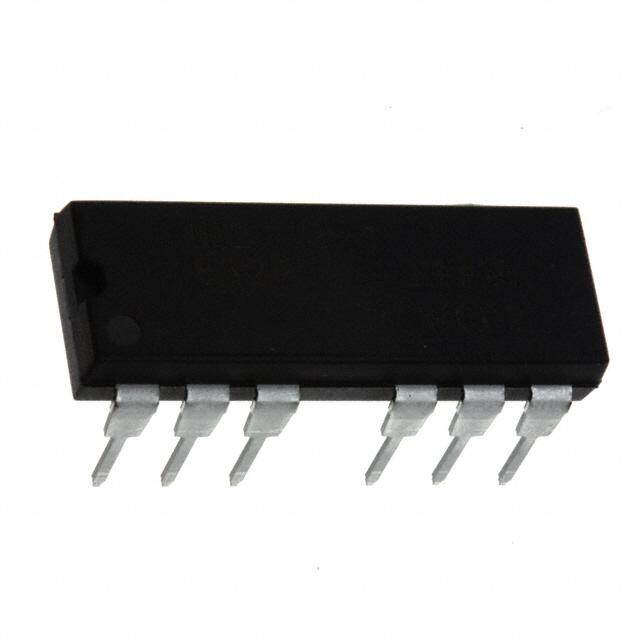
| 描述 | IC DRIVER MOSF HI/LOW SIDE 8SOIC门驱动器 Low Cost High Side MOSFET Predriver - Lead Free |
| 产品分类 | PMIC - MOSFET,电桥驱动器 - 外部开关集成电路 - IC |
| 品牌 | Micrel |
| 产品手册 | |
| 产品图片 |
|
| rohs | 符合RoHS无铅 / 符合限制有害物质指令(RoHS)规范要求 |
| 产品系列 | 电源管理 IC,门驱动器,Micrel MIC5014YM- |
| 数据手册 | |
| 产品型号 | MIC5014YM |
| 产品 | MOSFET Gate Drivers |
| 产品目录页面 | |
| 产品种类 | 门驱动器 |
| 供应商器件封装 | 8-SOIC |
| 其它名称 | 576-2352 |
| 包装 | 管件 |
| 商标 | Micrel |
| 安装类型 | 表面贴装 |
| 安装风格 | SMD/SMT |
| 封装 | Tube |
| 封装/外壳 | 8-SOIC(0.154",3.90mm 宽) |
| 封装/箱体 | SOIC-8 |
| 工作温度 | -40°C ~ 85°C |
| 工厂包装数量 | 95 |
| 延迟时间 | 2.5ms |
| 最大关闭延迟时间 | 30 us |
| 最大工作温度 | + 85 C |
| 最大开启延迟时间 | 8 ms |
| 最小工作温度 | - 40 C |
| 标准包装 | 95 |
| 电压-电源 | 2.75 V ~ 30 V |
| 电流-峰值 | - |
| 电源电压-最大 | 30 V |
| 电源电压-最小 | 2.75 V |
| 类型 | Low Cost High or Low Side MOSFET Driver |
| 系列 | MIC5014 |
| 输入类型 | 非反相 |
| 输出数 | 1 |
| 输出端数量 | 1 |
| 配置 | Non-Inverting |
| 配置数 | 1 |
| 高压侧电压-最大值(自举) | - |


- 商务部:美国ITC正式对集成电路等产品启动337调查
- 曝三星4nm工艺存在良率问题 高通将骁龙8 Gen1或转产台积电
- 太阳诱电将投资9.5亿元在常州建新厂生产MLCC 预计2023年完工
- 英特尔发布欧洲新工厂建设计划 深化IDM 2.0 战略
- 台积电先进制程称霸业界 有大客户加持明年业绩稳了
- 达到5530亿美元!SIA预计今年全球半导体销售额将创下新高
- 英特尔拟将自动驾驶子公司Mobileye上市 估值或超500亿美元
- 三星加码芯片和SET,合并消费电子和移动部门,撤换高东真等 CEO
- 三星电子宣布重大人事变动 还合并消费电子和移动部门
- 海关总署:前11个月进口集成电路产品价值2.52万亿元 增长14.8%


PDF Datasheet 数据手册内容提取
MIC5014/5015 Micrel, Inc. MIC5014/5015 Low-Cost High- or Low-Side MOSFET Driver General Description Features MIC5014 and MIC5015 MOSFET drivers are designed for • 2.75V to 30V operation gate control of N-channel, enhancement-mode, power • 100µA maximum supply current (5V supply) MOSFETs used as high-side or low-side switches. • 15µA typical off-state current The MIC5014/5 can sustain an on-state output indefinitely. • Internal charge pump • TTL compatible input The MIC5014/5 operates from a 2.75V to 30V supply. In high- • Withstands 60V transient (load dump) side configurations, the driver can control MOSFETs that • Reverse battery protected to –20V switch loads of up to 30V. In low-side configurations, with • Inductive spike protected to –20V separate supplies, the maximum switched voltage is limited • Overvoltage shutdown at 35V only by the MOSFET. • Internal 15V gate protection The MIC5014/5 has a TTL compatible control input. • Minimum external parts The MIC5014 is noninverting while the MIC5015 is inverting. • Operates in high-side or low-side configurations The MIC5014/5 features an internal charge pump that can • 1µA control input pull-off sustain a gate voltage greater than the available supply • Inverting and noninverting versions voltage. The driver is capable of turning on a logic-level MOSFET from a 2.75V supply or a standard MOSFET from a Applications 5V supply. The gate-to-source output voltage is internally limited to approximately 15V. • Automotive electrical load control The MIC5014/5 is protected against automotive load dump, • Battery-powered computer power management reversed battery, and inductive load spikes of –20V. • Lamp control The driver’s overvoltage shutdown feature turns off the exter- • Heater control nal MOSFET at approximately 35V to protect the load against • Motor control power supply excursions. • Power bus switching The MIC5014 is an improved pin-for-pin compatible replace- ment in many MIC5011 applications. The MIC5014/5 is available in plastic 8-pin DIP and 8-pin SOIC pacakges. Typical Application +3V to +4V 10µF MIC5014 1 8 V+ NC Control Input 2 7 ON Input NC OFF 3 6 Source NC 4 Gnd Gate 5 IRLZ24 d a o L Figure 1. 3V “Sleep-Mode” Switch with a Logic-Level MOSFET Micrel, Inc. • 2180 Fortune Drive • San Jose, CA 95131 • USA • tel + 1 (408) 944-0800 • fax + 1 (408) 474-1000 • http://www.micrel.com June 2005 1 MIC5014/5015
MIC5014/5015 Micrel, Inc. Ordering Information Part Number Temperature Standard Pb-Free Range Configuration Package MIC5014BM MIC5014YM –40ºC to +85ºC Non-Inverting 8-Pin SOIC MIC5014BN MIC5014YN –40ºC to +85ºC Non-Inverting 8-Pin PDIP MIC5015BM MIC5015YM –40ºC to +85ºC Inverting 8-Pin SOIC MIC5015BN MIC5015YN –40ºC to +85ºC Inverting 8-Pin PDIP Block Diagram V+ (1) Charge Pump Gate (5) 15V Source (3) Input (2) * * Only on the inverting version Ground (4) Pin Description Pin Number Pin Name Pin Function 1 V+ Supply. Must be decoupled to isolate from large transients caused by the power MOSFET drain. 10µF is recommended close to pins 1 and 4. 2 Input Turns on power MOSFET when taken above (or below) threshold (1.0V typical). Pin 2 requires ~ 1µA to switch. 3 Source Connects to source lead of power MOSFET and is the return for the gate clamp zener. Pin 3 can safely swing to –20V when turning off inductive loads. 4 Ground 5 Gate Drives and clamps the gate of the power MOSFET. 6, 7, 8 NC Not internally connected. MIC5014/5015 2 June 2005
MIC5014/5015 Micrel, Inc. Absolute Maximum Ratings Operating Ratings (Notes 1,2) (Notes 1,2) Supply Voltage...............................................–20V to 60V θ (Plastic DIP).....................................................160°C/W JA Input Voltage.....................................................–20V to V+ θ (SOIC) .............................................................170°C/W JA Source Voltage..................................................–20V to V+ Ambient Temperature: ................................–40°C to +85°C Source Current..........................................................50mA Storage Temperature................................–65°C to +150°C Gate Voltage..................................................–20V to 50V Lead Temperature......................................................260°C Junction Temperature.............................................. 150°C (max soldering time: 10 seconds) Supply Voltage (V+).........................................2.75V to 30V Electrical Characteristics (Note 3) T = –40°C to +85°C unless otherwise specified A Parameter Conditions Min Typ Max Units Supply Current V+ = 30V V De-Asserted (Note 5) 10 25 µA IN V Asserted (Note 5) 5.0 10 mA IN V+ = 5V V De-Asserted 10 25 IN µA V Asserted 60 100 IN V+ = 3V V De-Asserted 10 25 IN µA V Asserted 25 35 IN Logic Input Voltage Threshold 3.0V ≤ V+ ≤ 30V Digital Low Level 0.8 V V T = 25°C Digital High Level 2.0 IN A Logic Input Current 3.0V ≤ V+ ≤ 30V V Low –2.0 0 IN µA MIC5014 (non-inverting) V High 1.0 2.0 IN Logic Input Current 3.0V ≤ V+ ≤ 30V V Low –2.0 –1.0 IN µA MIC5015 (inverting) V High –1.0 2.0 IN Input Capacitance 5.0 pF Gate Enhancement 3.0V ≤ V+ ≤ 30V V Asserted 4.0 17 V IN V – V GATE SUPPLY Zener Clamp 8.0V ≤ V+ ≤ 30V V Asserted 13 15 17 V IN V – V GATE SOURCE Gate Turn-on Time, t V+ = 4.5V V switched on, measure 2.5 8.0 ms ON IN (Note 4) C = 1000pF time for V to reach V+ + 4V L GATE V+ = 12V As above, measure time for 90 140 µs C = 1000pF V to reach V+ + 4V L GATE Gate Turn-off Time, t V+ = 4.5V V switched off, measure 6.0 30 µs OFF IN (Note 4) C = 1000pF time for V to reach 1V L GATE V+ = 12V As above, measure time for 6.0 30 µs C = 1000pF V to reach 1V L GATE Overvoltage Shutdown 35 37 41 V Threshold Note 1: Absolute Maximum Ratings indicate limits beyond which damage to the device may occur. Electrical specifications do not apply when operating the device beyond its specified Operating Ratings. Note 2: The MIC5014/5015 is ESD sensitive. Note 3: Minimum and maximum Electrical Characteristics are 100% tested at TA = 25°C and TA = 85°C, and 100% guaranteed over the entire operating temperature range. Typicals are characterized at 25°C and represent the most likely parametric norm. Note 4: Test conditions reflect worst case high-side driver performance. Low-side and bootstrapped topologies are significantly faster—see Applications Information. Note 5: “Asserted” refers to a logic high on the MIC5014 and a logic low on the MIC5015. June 2005 3 MIC5014/5015
MIC5014/5015 Micrel, Inc. Typical Characteristics All data measured using FET probe to minimize resistive loading Supply Current Gate Enhancement High-Side Turn-On Time (Output Asserted) vs. Supply Voltage vs. Gate Capacitance 6 20 300 NT (mA)45 MENT (V)15 E (s)µ220500 Y CURRE23 NHANCE10 N-ON TIM110500 L E R SUPP1 GATE 5 GVate E –n hVancement = TU 50 Supply = 12V GATE SUPPLY 0 0 0 0 5 10 15 20 25 30 0 5 10 15 20 25 30 0 2 4 6 8 10 SUPPLY VOLTAGE (V) SUPPLY VOLTAGE (V) GATE CAPACITANCE (nF) High-Side Turn-On Time High-Side Turn-On Time High-Side Turn-On Time Until Gate = Supply + 4V Until Gate = Supply + 4V vs. Temperature 100 100 180 s) ms) 10 CGATE = 1300pF ms) 10 CGATE = 3000pF TIME (µ114600 E ( E ( N 120 M M O TURN-ON TI 0.11 TURN-ON TI 0.11 H-SIDE TURN-104680000 SCuGpApTEly = = 1 1020V0pF G 20 0.01 0.01 HI 0 0 4 8 12 16 20 24 28 0 4 8 12 16 20 24 28 -60 -30 0 30 60 90 120 150 SUPPLY VOLTAGE (V) SUPPLY VOLTAGE (V) AMBIENT TEMPERATURE (°C) High-Side Turn-On Time High-Side Turn-On Time High-Side Turn-Off Time Until Gate = Supply + 10V Until Gate = Supply + 10V Until Gate = 1V 100 100 10 N TIME (ms) 110 CGATE = 1300pF N TIME (ms) 110 CGATE = 3000pF FF TIME (s)µ 68 CGATE = 3000pF O O O 4 N- N- N- TUR 0.1 TUR 0.1 TUR 2 C = GATE 1300pF 0.01 0.01 0 0 5 10 15 20 25 30 0 5 10 15 20 25 30 0 5 10 15 20 25 30 SUPPLY VOLTAGE (V) SUPPLY VOLTAGE (V) SUPPLY VOLTAGE (V) Charge-Pump Charge-Pump Low-Side Turn-On Time Output Current Output Current Until Gate = 4V 1000 10000 10000 28V A) 28V A) CGATE = 3000pF URRENT (µ 100 12V URRENT (µ 1100000 Stvooo lgutarrogcueen cados:n snnuoeptceptdelyd12V N TIME (s)µ 1100000 C C O UTPUT 10 5V 3V Stoo suurcpep lcyo: nsunpepctlyed UTPUT 10 3V 5V TURN- 10 CGATE = 1300pF O voltage as noted O 1 1 1 0 5 10 15 0 5 10 15 0 5 10 15 20 25 30 GATE-TO-SOURCE VOLTAGE (V) GATE-TO-SOURCE VOLTAGE (V) SUPPLY VOLTAGE (V) MIC5014/5015 4 June 2005
MIC5014/5015 Micrel, Inc. Applications Information not use a socket for the MOSFET. If the MOSFET is a TO-220 type package, make high current connections to the drain tab. Functional Description Wiring losses have a profound effect on high-current circuits. The MIC5014 is functionally and pin for pin compatible with A floating milliohmeter can identify connections that are con- the MIC5011, except for the omission of the optional speed- tributing excess drop under load. up capacitor pins, which are available on the MIC5011. The MIC5015 is an inverting configuration of the MIC5014. Low Voltage Testing As the MIC5014/MIC5015 have relatively high output imped- The internal functions of these devices are controlled via a ances, a normal oscilloscope probe will load the device. This logic block (refer to block diagram) connected to the control is especially pronounced at low voltage operation. It is recom- input (pin 2). When the input is off (low for the MIC5014, and mended that a FET probe or unity gain buffer be used for all high for the MIC5015), all functions are turned off, and the testing. gate of the external power MOSFET is held low via two N- channel switches. This results in a very low standby current; Circuit Topologies 15µA typical, which is necessary to power an internal bandgap. The MIC5014 and MIC5015 are well suited for use with When the input is driven to the “ON” state, the N-channel standard power MOSFETs in both low and high side driver switches are turned off, the charge pump is turned on, and the configurations. In addition, the lowered supply voltage re- P-channel switch between the charge pump and the gate quirements of these devices make them ideal for use with logic turns on, allowing the gate of the power FET to be charged. level FETs in high side applications with a supply voltage of 3 The op amp and internal zener form an active regulator which to 4V. (If higher supply voltages [>4V] are used with logic level shuts off the charge pump when the gate voltage is high FETs, an external zener clamp must be supplied to ensure enough. This is a feature not found on the MIC5011. that the maximum V rating of the logic FET [10V] is not GS exceeded.) In addition, a standard IGBT can be driven using The charge pump incorporates a 100kHz oscillator and on- these devices. chip pump capacitors capable of charging a 1,000pF load in 90µs typical. In addition to providing active regulation, the Choice of one topology over another is usually based on internal 15V zener is included to prevent exceeding the V GS speed vs. safety. The fastest topology is the low side driver, rating of the power MOSFET at high supply voltages. however, it is not usually considered as safe as high side driving as it is easier to accidentally short a load to ground than The MIC5014/15 devices have been improved for greater to V The slowest, but safest topology is the high side ruggedness and durability. All pins can withstand being CC. driver; with speed being inversely proportional to supply pulled 20V below ground without sustaining damage, and the voltage. It is the preferred topology for most military and supply pin can withstand an overvoltage transient of 60V for automotive applications. Speed can be improved consider- 1s. An overvoltage shutdown has also been included, which ably by bootstrapping from the supply. turns off the device when the supply exceeds 35V. All topologies implemented using these devices are well Construction Hints suited to driving inductive loads, as either the gate or the High current pulse circuits demand equipment and assembly source pin can be pulled 20V below ground with no effect. techniques that are more stringent than normal, low current External clamp diodes are unnecessary, except for the case lab practices. The following are the sources of pitfalls most in which a transient may exceed the overvoltage trip point. often encountered during prototyping: Supplies : Many bench power supplies have poor transient response. Circuits that High Side Driver (Figure 1) The high side topology shown are being pulse tested, or those that operate by pulse-width here is an implementation of a “sleep-mode” switch for a modulation will produce strange results when used with a laptop or notebook computer which uses a logic level FET. A supply that has poor ripple rejection, or a peaked transient standard power FET can easily be substituted when supply response. Always monitor the power supply voltage that voltages above 4V are required. appears at the drain of a high side driver (or the supply side +3V to +30V of the load for a low side driver) with an oscilloscope. It is not uncommon to find bench power supplies in the 1kW class that 10µF overshoot or undershoot by as much as 50% when pulse MIC5014 loaded. Not only will the load current and voltage measure- 1 V+ NC 8 ad ments be affected, but it is possible to overstress various Control Input 2 7 Lo ON Input NC components, especially electrolytic capacitors, with possibly OFF 3 6 Source NC catastrophic results. A 10µF supply bypass capacitor at the 4 Gnd Gate 5 chip is recommended. Residual resistances: Resistances in circuit connections may also cause confusing results. For example, a circuit may employ a 50mΩ power MOSFET for low voltage drop, but unless careful construction techniques are used, one could easily add 50 to 100mΩ resistance. Do Figure 2. Low Side Driver June 2005 5 MIC5014/5015
MIC5014/5015 Micrel, Inc. Low Side Driver (Figure 2) A key advantage of this topology, the short is removed, feedback to the input pin insures that the as previously mentioned, is speed. The MOSFET gate is MIC5014 will turn back on. This output can also be level driven to near supply immediately when the MIC5014/15 is shifted and sent to an I/O port of a microcontroller for intelli- turned on. Typical circuits reach full enhancement in 50µs or gent control. less with a 15V supply. Current Shunts (R ). Low valued resistors are necessary for S Bootstrapped High Side Driver (Figure 3) The turn-on time of use at R . Resistors are available with values ranging from 1 S a high side driver can be improved to faster than 40µs by to 50mΩ, at 2 to 10W. If a precise overcurrent trip point is bootstrapping the supply with the MOSFET source. The not necessary, then a nonprecision resistor or even a mea- Schottky barrier diode prevents the supply pin from dropping sured PCB trace can serve as R . The major cause of drift in S more than 200mV below the drain supply and improves turn- resistor values with such resistors is temperature coefficient; on time. Since the supply current in the “off” state is only a the designer should be aware that a linear, 500 ppm/°C small leakage, the 100nF bypass capacitor tends to remain change will contribute as much as 10% shift in the overcurrent charged for several seconds after the MIC5014/15 is turned trip point. If this is not acceptable, a power resistor designed off. Faster speeds can be obtained at the expense of supply for current shunt service (drifts less than 100 ppm/°C), or a voltage (the overvoltage shutdown will turn the part off when Kelvin-sensed resistor may be used.† the bootstrapping action pulls the supply pin above 35V) by 12V using a larger capacitor at the junction of the two 1N4001 diodes. In a PWM application (this circuit can be used for either PWM’ed or continuously energized loads), the chip supply is On sustained at a higher potential than the system supply, which I = V /R TRIP TRIP S improves switching time. = 1.7A +2.75V to +30V 10µF VTRIP = R1/(R1+R2) MIC5014 1N5817 1 V+ NC 8 R0.S06Ω R1k1Ω 2 7 Input NC 1N4001 (2) 3 6 R4 Source NC 1kΩ 100nF 4 Gnd Gate 5 1µF MIC5015 LM301A 1 V+ NC 8 ad R1220kΩ 2.2kΩ Control Input 2 7 Lo ON Input NC OFF 3 6 Source NC 4 Gnd Gate 5 1RF540 Figure 4. High Side Driver with Overcurrent Shutdown † Suppliers of Precision Power Resistors: d Dale Electronics, Inc., 2064 12th Ave., Columbus, NE 68601. (402) 565- a Lo 3131 International Resistive Co., P.O. Box 1860, Boone,NC 28607-1860. (704) 264-8861 Isotek Corp., 566 Wilbur Ave. Swansea, MA 02777. (508) 673-2900 Figure 3. Bootstrapped Hgh-Side Driver Kelvin, 14724 Ventura Blvd., Ste. 1003, Sherman Oaks, CA 91403-3501. (818) 990-1192 RCD Components, Inc., 520 E. Industrial Pk. Dr., Manchester, NH 03103. High Side Driver With Current Sense (Figure 4) Although no (603) 669-0054 current sense function is included on the MIC5014/15 devices, Ultronix, Inc., P.O. Box 1090, Grand Junction, CO 81502 (303) 242-0810 a simple current sense function can be realized via the addition High Side Driver With Delayed Current Sense (Figure 5) of one more active component; an LM301A op amp used as Delay of the overcurrent detection to accomodate high inrush a comparator. The positive rail of the op amp is tied to V+, and loads such as incandescent or halogen lamps can be accom- the negative rail is tied to ground. This op amp was chosen as plished by adding an LM3905 timer as a one shot to provide it can withstand having input transients that swing below the an open collector pulldown for the comparator output such negative rail, and has common mode range almost to the that the control input of the MIC5015 stays low for a preset positive rail. amount of time without interference from the current sense The inverting side of this comparator is tied to a voltage divider circuitry. Note that an MIC5015 must be used in this applica- which sets the voltage to V+ – V . The non inverting side tion (figure 5), as an inverting control input is necessary. The TRIP is tied to the node between the drain of the FET and the sense delay time is set by the RC time constant of the external resistor. If the overcurrent trip point is not exceeded , this node components on pins 3 and 4 of the timer; in this case, 6ms was will always be pulled above V+ – V , andthe output of the chosen. TRIP comparator will be high which feeds the control input of the An LM3905 timer was used instead of a 555 as it provides a MIC5014 (polarities should be reversed if the MIC5015 is clean transition, and is almost impossible to make oscillate. used). One the overcurrent trip point has been reached, the Good bypassing and noise immunity is essential in this circuit comparator will go low, which shuts off the MIC5014. When the to prevent spurious op amp oscillations. MIC5014/5015 6 June 2005
MIC5014/5015 Micrel, Inc. 12V 12V LM3905N 1 8 Trigger Logic 2 7 On V Emit REF 3 6 R/C Coll 10µF 4 Gnd V+ 5 MIC5014 1 V+ NC 8 R0.S06Ω R1k1Ω 2 7 Input NC 1000pF 3 6 R4 0.01µF Source NC 1kΩ 4 Gnd Gate 5 R2 LM301A ad 120kΩ 2.2kΩ o 1kΩ L Figure 5. High Side Driver with Delayed Overcurrent Shutdown Typical Applications Variable Supply Low Side Driver for Motor Speed Control applications, it is acceptable to allow this voltage to momen- (Figure 6) The internal regulation in the MIC5014/15 allows tarily turn the MOSFET back on as a way of dissipating the a steady gate enhancement to be supplied while the inductor’s current. However, if this occurs when driving a MIC5014/15 supply varies from 5V to 30V, without damaging solenoid valve with a fast switching speed, chemicals or the internal gate to source zener clamp. This allows the speed gases may be inadvertantly be dispensed at the wrong time of the DC motor shown to be varied by varying the supply with possibly disasterous consequences. Also, too large of voltage. a kickback voltage (as is found in larger solenoids) can damage the MIC5014 or the power FET by forcing the Source V = +5V to +30V node below ground (the MIC5014 can be driven up to 20V CC below ground before this happens). A catch diode has been included in this design to provide an alternate route for the MIC5014 inductive kickback current to flow. The 5kΩ resistor in series 1 V+ NC 8 with this diode has been included to set the recovery time of 2 7 M the solenoid valve. ON Input NC OFF 3 6 24V Source NC 4 Gnd Gate 5 IRF540 MIC5015 1 8 V+ NC 2 7 OFF Input NC ON 3 6 Source NC 4 Gnd Gate 5 IRFZ40 Figure 6: DC Motor Speed Control/Driver Solenoid Valve Driver (Figure 7) High power solenoid valves are used in many industrial applications requiring the timed ASCO 1N4005 8320A dispensing of chemicals or gases. When the solenoid is Solenoid 5kΩ activated, the valve opens (or closes), releasing (or stopping) fluid flow. A solenoid valve, like all inductive loads, has a considerable “kickback” voltage when turned off, as current cannot change instantaneously through an inductor. In most Figure 7: Solenoid Valve Driver June 2005 7 MIC5014/5015
MIC5014/5015 Micrel, Inc. Incandescent/Halogen Lamp Driver (Figure 8) The combi- Motor Driver With Stall Shutdown (Figure 10) Tachometer nation of an MIC5014/5015 and a power FET makes an feedback can be used to shut down a motor driver circuit when effective driver for a standard incandescent or halogen lamp a stall condition occurs. The control switch is a 3-way type; the load. Such loads often have high inrush currents, as the “START” position is momentary and forces the driver ON. resistance of a cold filament is less than one-tenth as much as When released, the switch returns to the “RUN” position, and when it is hot. Power MOSFETs are well suited to this the tachometer’s output is used to hold the MIC5014 input ON. application as they have wider safe operating areas than do If the motor slows down, the tach output is reduced, and the power bipolar transistors. It is important to check the SOA MIC5014 switches OFF. Resistor “R” sets the shutdown curve on the data sheet of the power FET to be used against threshold. the estimated or measured inrush current of the lamp in question prior to prototyping to prevent “explosive” results. 12V If overcurrent sense is to be used, first measure the duration of the inrush, then use the topology of Figure 5 with the RC of 10µF the timer chosen to accomodate the duration with suitable MIC5014 1 8 V+ NC guardbanding. 12V 2 Input NC 7 330kΩ 3 6 Source NC 10µF 4 Gnd Gate 5 IRFZ44 MIC5014 R 1 8 330kΩ V+ NC Control Input 2 7 ON Input NC OFF 3 6 1N4148 Source NC T M 4 Gnd Gate 5 IRF540 Figure 10. Motor Stall Shutdowm OSRAM HLX64623 Figure 8. Halogen Lamp Driver Simple DC-DC Converter (Figure 11) The simplest applica- tion for the MIC5014 is as a basic one-chip DC-DC converter. As the output (Gate) pin has a relatively high impedance, the Relay Driver (Figure 9) Some power relay applications re- output voltage shown will vary significantly with applied load. quire the use of a separate switch or drive control, such as in the case of microprocessor control of banks of relays where a logic level control signal is used, or for drive of relays with high power requirements. The combination of an MIC5014/ 5V 5015 and a power FET also provides an elegant solution to power relay drive. 10µF MIC5014 1 8 V+ NC 12V 2 7 Input NC 3 6 Source NC 10µF MIC5014 4 Gnd Gate 5 V = 12V 1 8 OUT V+ NC Control Input 2 7 ON Input NC OFF 3 6 Source NC 4 Gnd Gate 5 IRF540 Guardian Electric Figure 11. DC - DC Converter 1725-1C-12D Figure 9: Relay Driver MIC5014/5015 8 June 2005
MIC5014/5015 Micrel, Inc. High Side Driver With Load Protection (Figure 12) Al- The addition of a Schottky diode between the supply and the though the MIC5014/15 devices are reverse battery pro- FET eliminates this problem. The MBR2035CT was chosen tected, the load and power FET are not, in a typical high side as it can withstand 20A continuous and 150A peak, configuration. In the event of a reverse battery condition, the and should survive the rigors of an automotive environment. internal body diode of the power FET will be forward biased. The two diodes are paralleled to reduce switch loss (forward This allows the reversed supply access to the load. voltage drop). 12V 10µF MBR2035CT MIC5014 1 8 V+ NC Control Input 2 7 ON Input NC OFF 3 6 Source NC 4 Gnd Gate 5 IRF540 d a o L Figure 12: High Side Driver WIth Load Protection Push-Pull Driver With No Cross-Conduction (Figure 13) considerable deadtime (time when neither driver is turned on). As the turn-off time of the MIC5014/15 devices is much faster If this circuit is used to drive an inductive load, catch diodes than the turn-on time, a simple push-pull driver with no cross must be used on each half to provide an alternate path for the conduction can be made using one MIC5014 and one kickback current that will flow during this deadtime. MIC5015. The same control signal is applied to both inputs; the MIC5014 turns on with the positive signal, and the This circuit is also a simple half H-bridge which can be driven MIC5015 turns on when it swings low. with a PWM signal on the input for SMPS or motor drive This scheme works with no additional components as the applications in which high switching frequencies are not relative time difference between the rise and fall times of the desired. MIC5014 is large. However, this does mean that there is 12V 10µF MIC5014 1 8 V+ NC 2 7 Input NC 3 6 Source NC 4 Gnd Gate 5 IRFZ40 Control Input 12V V OUT MIC5015 1 8 V+ NC 2 7 Input NC 3 6 Source NC 4 Gnd Gate 5 IRFZ40 Figure 13: Push-Pull Driver June 2005 9 MIC5014/5015
MIC5014/5015 Micrel, Inc. Package Information PIN 1 DIMENSIONS:(cid:0) INCH (MM) 0.380 (9.65)(cid:0) 0.255 (6.48)(cid:0) 0.370 (9.40) 0.135 (3.43)(cid:0) 0.245 (6.22) 0.125 (3.18) 0.300 (7.62) 0.013 (0.330)(cid:0) 0.010 (0.254) 0.018 (0.57) 0.130 (3.30) 0.380 (9.65)(cid:0) 0.320 (8.13)(cid:0) 0.100 (2.54) 0.0375 (0.952) (cid:0) 8-Pin Plastic DIP (N) 0.026 (0.65)(cid:0) MAX) PIN 1 0.157 (3.99)(cid:0) DIMENSIONS:(cid:0) 0.150 (3.81) INCHES (MM) 0.020 (0.51)(cid:0) 0.013 (0.33) 0.050 (1.27)(cid:0) TYP 0.0098 (0.249)(cid:0) 45° 0.010 (0.25)(cid:0) 0.0040 (0.102) 0.007 (0.18) 0.197 (5.0)(cid:0) 0°–8° 0.050 (1.27)(cid:0) 0.064 (1.63)(cid:0) 0.189 (4.8) SEATING(cid:0) 0.016 (0.40) 0.045 (1.14) PLANE 0.244 (6.20)(cid:0) 0.228 (5.79) 8-Pin SOP (M) MIC5014/5015 10 June 2005
MIC5014/5015 Micrel, Inc. June 2005 11 MIC5014/5015
MIC5014/5015 Micrel, Inc. MICREL INC. 2180 FORTUNE DRIVE SAN JOSE, CA 95131 USA TEL + 1 (408) 944-0800 FAX + 1 (408) 474-1000 WEB http://www.micrel.com This information furnished by Micrel in this data sheet is believed to be accurate and reliable. However no responsibility is assumed by Micrel for its use. Micrel reserves the right to change circuitry and specifications at any time without notification to the customer. Micrel Products are not designed or authorized for use as components in life support appliances, devices or systems where malfunction of a product can reasonably be expected to result in personal injury. Life support devices or systems are devices or systems that (a) are intended for surgical implant into the body or (b) support or sustain life, and whose failure to perform can be reasonably expected to result in a significant injury to the user. A Purchaser’s use or sale of Micrel Products for use in life support appliances, devices or systems is a Purchaser’s own risk and Purchaser agrees to fully indemnify Micrel for any damages resulting from such use or sale. © 1997 Micrel Incorporated MIC5014/5015 12 June 2005
Mouser Electronics Authorized Distributor Click to View Pricing, Inventory, Delivery & Lifecycle Information: M icrochip: MIC5014YM MIC5015YN MIC5015YM MIC5014YN MIC5015YM-TR MIC5014YM-TR