ICGOO在线商城 > 集成电路(IC) > 时钟/计时 - 可编程计时器和振荡器 > MC14541BDR2G
 Datasheet下载
- 型号: MC14541BDR2G
- 制造商: ON Semiconductor
- 库位|库存: xxxx|xxxx
- 要求:
| 数量阶梯 | 香港交货 | 国内含税 |
| +xxxx | $xxxx | ¥xxxx |
查看当月历史价格
查看今年历史价格
MC14541BDR2G产品简介:
ICGOO电子元器件商城为您提供MC14541BDR2G由ON Semiconductor设计生产,在icgoo商城现货销售,并且可以通过原厂、代理商等渠道进行代购。 MC14541BDR2G价格参考¥0.88-¥1.17。ON SemiconductorMC14541BDR2G封装/规格:时钟/计时 - 可编程计时器和振荡器, Programmable Timer IC 3MHz 14-SOIC。您可以下载MC14541BDR2G参考资料、Datasheet数据手册功能说明书,资料中有MC14541BDR2G 详细功能的应用电路图电压和使用方法及教程。
ON Semiconductor(安森美)的MC14541BDR2G是一款可编程振荡器/定时器,属于时钟/计时类器件,广泛应用于需要精确时间控制或频率生成的电子系统中。该器件基于14位二进制计数器和可编程逻辑设计,能够实现从外部电阻电容(RC)网络设定的振荡频率,并通过内部分频输出多种定时信号。

典型应用场景包括:

1. 工业控制:用于定时控制继电器、电机启停、PLC模块中的延时功能等,提供稳定可靠的定时基准。
2. 消费电子:在家电(如洗衣机、微波炉)中作为延时开关或周期性控制信号源。
3. 电源管理:用于开关电源或DC-DC转换器中的软启动电路,控制上电延迟时间,防止电流冲击。
4. 通信设备:为低速通信接口提供时钟信号或看门狗定时功能,增强系统稳定性。
5. 汽车电子:应用于车身控制模块,如车灯延时关闭、雨刷间歇控制等,满足汽车级可靠性和温度范围要求。
6. 仪器仪表:作为测量设备中的时间基准单元,实现周期性采样或信号触发。

MC14541BDR2G采用SOIC-14封装,符合RoHS标准,具备高抗干扰能力和宽工作电压范围(3V至18V),适合多种电源环境。其可编程特性使其无需晶振即可实现灵活的定时配置,降低成本与元件数量,是替代传统555定时器的更稳定、精度更高的选择。
| 参数 | 数值 |
| 产品目录 | 集成电路 (IC)半导体 |
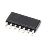
| 描述 | IC OSC PROG TIMER 3MHZ 14SOIC计时器和支持产品 LOG CMOS OSILATR TIMER |
| 产品分类 | |
| 品牌 | ON Semiconductor |
| 产品手册 | |
| 产品图片 |
|
| rohs | 符合RoHS无铅 / 符合限制有害物质指令(RoHS)规范要求 |
| 产品系列 | 时钟和计时器IC,计时器和支持产品,ON Semiconductor MC14541BDR2G- |
| 数据手册 | |
| 产品型号 | MC14541BDR2G |
| 产品目录页面 | |
| 产品种类 | 计时器和支持产品 |
| 传播延迟—最大值 | 18000 ns, 10000 ns, 7500 ns |
| 供应商器件封装 | 14-SOICN |
| 其它名称 | MC14541BDR2GOSDKR |
| 内部定时器数量 | 1 |
| 包装 | Digi-Reel® |
| 商标 | ON Semiconductor |
| 安装类型 | 表面贴装 |
| 安装风格 | SMD/SMT |
| 封装 | Reel |
| 封装/外壳 | 14-SOIC(0.154",3.90mm 宽) |
| 封装/箱体 | SOIC-14 |
| 工作温度 | -55°C ~ 125°C |
| 工厂包装数量 | 2500 |
| 最大功率耗散 | 500 mW |
| 最大工作温度 | + 125 C |
| 最小工作温度 | - 55 C |
| 标准包装 | 1 |
| 电压-电源 | 3 V ~ 18 V |
| 电流-电源 | 15µA |
| 电源电压-最大 | 18 V |
| 电源电压-最小 | 3 V |
| 类型 | 可编程计时器 |
| 系列 | MC14541B |
| 计数 | - |
| 频率 | 3MHz |


- 商务部:美国ITC正式对集成电路等产品启动337调查
- 曝三星4nm工艺存在良率问题 高通将骁龙8 Gen1或转产台积电
- 太阳诱电将投资9.5亿元在常州建新厂生产MLCC 预计2023年完工
- 英特尔发布欧洲新工厂建设计划 深化IDM 2.0 战略
- 台积电先进制程称霸业界 有大客户加持明年业绩稳了
- 达到5530亿美元!SIA预计今年全球半导体销售额将创下新高
- 英特尔拟将自动驾驶子公司Mobileye上市 估值或超500亿美元
- 三星加码芯片和SET,合并消费电子和移动部门,撤换高东真等 CEO
- 三星电子宣布重大人事变动 还合并消费电子和移动部门
- 海关总署:前11个月进口集成电路产品价值2.52万亿元 增长14.8%


PDF Datasheet 数据手册内容提取
MC14541B Programmable Timer The MC14541B programmable timer consists of a 16−stage binary counter, an integrated oscillator for use with an external capacitor and two resistors, an automatic power−on reset circuit, and output control logic. Timing is initialized by turning on power, whereupon the power−on http://onsemi.com reset is enabled and initializes the counter, within the specified V DD range. With the power already on, an external reset pulse can be applied. Upon release of the initial reset command, the oscillator will oscillate with a frequency determined by the external RC network. The 16−stage counter divides the oscillator frequency (f ) with the nth osc stage frequency being f /2n. SOIC−14 SOEIAJ−14 TSSOP−14 osc D SUFFIX F SUFFIX DT SUFFIX Features CASE 751A CASE 965 CASE 948G • Available Outputs 28, 210, 213 or 216 • PIN ASSIGNMENT Increments on Positive Edge Clock Transitions • Built−in Low Power RC Oscillator (±2% accuracy over temperature Rtc 1 14 VDD range and ±20% supply and ±3% over processing at < 10 kHz) • Ctc 2 13 B Oscillator May Be Bypassed if External Clock Is Available RS 3 12 A (Apply external clock to Pin 3) • NC 4 11 NC External Master Reset Totally Independent of Automatic Reset Operation AR 5 10 MODE • Operates as 2n Frequency Divider or Single Transition Timer MR 6 9 Q/Q SEL • Q/Q Select Provides Output Logic Level Flexibility VSS 7 8 Q • Reset (auto or master) Disables Oscillator During Resetting to NC = NO CONNECTION Provide No Active Power Dissipation • Clock Conditioning Circuit Permits Operation with Very Slow Clock MARKING DIAGRAMS Rise and Fall Times • Automatic Reset Initializes All Counters On Power Up 14 14 • Supply Voltage Range = 3.0 Vdc to 18 Vdc with Auto Reset 14541BG MC14541B Supply Voltage Range = Disabled (Pin 5 = V ) AWLYWW ALYWG DD Supply Voltage Range = 8.5 Vdc to 18 Vdc with Auto Reset 1 1 Supply Voltage Range = Enabled (Pin 5 = V ) SS SOIC−14 SOEIAJ−14 • NLV Prefix for Automotive and Other Applications Requiring Unique Site and Control Change Requirements; AEC−Q100 14 Qualified and PPAP Capable 14 • 541B These Devices are Pb−Free and are RoHS Compliant ALYW(cid:2) (cid:2) 1 TSSOP−14 A = Assembly Location WL, L = Wafer Lot YY, Y = Year WW, W = Work Week G or (cid:2) = Pb−Free Package (Note: Microdot may be in either location) ORDERING INFORMATION See detailed ordering and shipping information in the package dimensions section on page 2 of this data sheet. © Semiconductor Components Industries, LLC, 2014 1 Publication Order Number: July, 2014 − Rev. 14 MC14541B/D
MC14541B MAXIMUM RATINGS (Voltages Referenced to VSS) Symbol Parameter Value Unit VDD DC Supply Voltage Range −0.5 to +18.0 V Vin, Vout Input or Output Voltage Range, (DC or Transient) −0.5 to VDD + 0.5 V Iin Input Current (DC or Transient) ±10 (per Pin) mA Iout Output Current (DC or Transient) ±45 (per Pin) mA PD Power Dissipation, per Package (Note 1) 500 mW TA Ambient Temperature Range −55 to +125 °C Tstg Storage Temperature Range −65 to +150 °C TL Lead Temperature, (8−Second Soldering) 260 °C Stresses exceeding those listed in the Maximum Ratings table may damage the device. If any of these limits are exceeded, device functionality should not be assumed, damage may occur and reliability may be affected. 1. Temperature Derating: “D/DW” Packages: –7.0 mW/(cid:3)C From 65(cid:3)C To 125(cid:3)C ORDERING INFORMATION Device Package Shipping† MC14541BDG SOIC−14 55 Units / Rail (Pb−Free) NLV14541BDG* SOIC−14 55 Units / Rail (Pb−Free) MC14541BDR2G SOIC−14 2500 / Tape & Reel (Pb−Free) NLV14541BDR2G* SOIC−14 2500 / Tape & Reel (Pb−Free) MC14541BDTR2G TSSOP−14 2500 / Tape & Reel (Pb−Free) NLV14541BDTR2G* TSSOP−14 2500 / Tape & Reel (Pb−Free) MC14541BFELG SOEIAJ−14 2000 / Tape & Reel (Pb−Free) †For information on tape and reel specifications, including part orientation and tape sizes, please refer to our Tape and Reel Packaging Specifications Brochure, BRD8011/D. *NLV Prefix for Automotive and Other Applications Requiring Unique Site and Control Change Requirements; AEC−Q100 Qualified and PPAP Capable. http://onsemi.com 2
MC14541B ELECTRICAL CHARACTERISTICS (Voltages Referenced to VSS) − 55(cid:3)C 25(cid:3)C 125(cid:3)C VDD Characteristic Symbol Min Max Min Typ Max Min Max Unit Vdc (Note 2) Output Voltage “0” Level VOL 5.0 − 0.05 − 0 0.05 − 0.05 Vdc Vin = VDD or 0 10 − 0.05 − 0 0.05 − 0.05 15 − 0.05 − 0 0.05 − 0.05 “1” Level VOH 5.0 4.95 − 4.95 5.0 − 4.95 − Vdc Vin = 0 or VDD 10 9.95 − 9.95 10 − 9.95 − 15 14.95 − 14.95 15 − 14.95 − Input Voltage “0” Level VIL Vdc (VO = 4.5 or 0.5 Vdc) 5.0 − 1.5 − 2.25 1.5 − 1.5 (VO = 9.0 or 1.0 Vdc) 10 − 3.0 − 4.50 3.0 − 3.0 (VO = 13.5 or 1.5 Vdc) 15 − 4.0 − 6.75 4.0 − 4.0 “1” Level VIH Vdc (VO = 0.5 or 4.5 Vdc) 5.0 3.5 − 3.5 2.75 − 3.5 − (VO = 1.0 or 9.0 Vdc) 10 7.0 − 7.0 5.50 − 7.0 − (VO = 1.5 or 13.5 Vdc) 15 11 − 11 8.25 − 11 − Output Drive Current IOH mAdc (VOH = 2.5 Vdc) Source 5.0 –4.19 − –3.38 –6.75 − –2.37 − (VOH = 9.5 Vdc) 10 –7.96 − –6.42 –12.83 − –4.49 − (VOH = 13.5 Vdc) 15 –16.3 − –13.2 –26.33 − −9.24 − (VOL = 0.4 Vdc) Sink IOL 5.0 1.93 − 1.56 3.12 − 1.09 − mAdc (VOL = 0.5 Vdc) 10 4.96 − 4.0 8.0 − 2.8 − (VOL = 1.5 Vdc) 15 19.3 − 15.6 31.2 − 10.9 − Input Current Iin 15 − ±0.1 − ±0.00001 ±0.1 − ±1.0 (cid:2)Adc Input Capacitance Cin − − − − 5.0 7.5 − − pF (Vin = 0) Quiescent Current IDD 5.0 − 5.0 − 0.005 5.0 − 150 (cid:2)Adc (Pin 5 is High) 10 − 10 − 0.010 10 − 300 Auto Reset Disabled 15 − 20 − 0.015 20 − 600 Auto Reset Quiescent Current IDDR 10 − 250 − 30 250 − 1500 (cid:2)Adc (Pin 5 is low) 15 − 500 − 82 500 − 2000 Supply Current (Notes 3 & 4) ID 5.0 ID = (0.4 (cid:2)A/kHz) f + IDD (cid:2)Adc (Dynamic plus Quiescent) 10 ID = (0.8 (cid:2)A/kHz) f + IDD 15 ID = (1.2 (cid:2)A/kHz) f + IDD Product parametric performance is indicated in the Electrical Characteristics for the listed test conditions, unless otherwise noted. Product performance may not be indicated by the Electrical Characteristics if operated under different conditions. 2. Data labelled “Typ” is not to be used for design purposes but is intended as an indication of the IC’s potential performance. 3. The formulas given are for the typical characteristics only at 25(cid:3)C. 4. When using the on chip oscillator the total supply current (in (cid:2)Adc) becomes: IT = ID + 2 Ctc VDD f x 10–3 where ID is in (cid:2)A, Ctc is in pF, VDD in Volts DC, and f in kHz. (see Fig. 3) Dissipation during power−on with automatic reset enabled is typically 50 (cid:2)A @ VDD = 10 Vdc. http://onsemi.com 3
MC14541B SWITCHING CHARACTERISTICS (Note 5) (CL = 50 pF, TA = 25(cid:3)C) Characteristic Symbol VDD Min Typ Max Unit (Note 6) Output Rise and Fall Time tTLH, ns tTLH, tTHL = (1.5 ns/pF) CL + 25 ns tTHL 5.0 − 100 200 tTLH, tTHL = (0.75 ns/pF) CL + 12.5 ns 10 − 50 100 tTLH, tTHL = (0.55 ns/pF) CL + 9.5 ns 15 − 40 80 Propagation Delay, Clock to Q (28 Output) tPLH (cid:2)s tPLH, tPHL = (1.7 ns/pF) CL + 3415 ns tPHL 5.0 − 3.5 10.5 tPLH, tPHL = (0.66 ns/pF) CL + 1217 ns 10 − 1.25 3.8 tPLH, tPHL = (0.5 ns/pF) CL + 875 ns 15 − 0.9 2.9 Propagation Delay, Clock to Q (216 Output) tPHL (cid:2)s tPHL, tPLH = (1.7 ns/pF) CL + 5915 ns tPLH 5.0 − 6.0 18 tPHL, tPLH = (0.66 ns/pF) CL + 3467 ns 10 − 3.5 10 tPHL, tPLH = (0.5 ns/pF) CL + 2475 ns 15 − 2.5 7.5 Clock Pulse Width tWH(cl) 5.0 900 300 − ns 10 300 100 − 15 225 85 − Clock Pulse Frequency (50% Duty Cycle) fcl 5.0 − 1.5 0.75 MHz 10 − 4.0 2.0 15 − 6.0 3.0 MR Pulse Width tWH(R) 5.0 900 300 − ns 10 300 100 − 15 225 85 − Master Reset Removal Time trem 5.0 420 210 − ns 10 200 100 − 15 200 100 − 5. The formulas given are for the typical characteristics only at 25(cid:3)C. 6. Data labelled “Typ” is not to be used for design purposes but is intended as an indication of the IC’s potential performance. VDD VDD PULSE PULSE GENERATOR RS GENERATOR RS AR AR Q/Q SELECT Q/Q SELECT MODE Q MODE Q A CL A CL B B MR MR VSS VSS 20 ns 20 ns (Rtc AND Ctc OUTPUTS ARE LEFT OPEN) 90% 50% 50% 20 ns 20 ns RS 10% 90% tPLH tPHL 50% 10% 50% 90% 50% 50% Q 10% DUTY CYCLE tTLH tTHL Figure 1. Power Dissipation Test Circuit Figure 2. Switching Time Test Circuit and Waveform and Waveforms http://onsemi.com 4
MC14541B EXPANDED BLOCK DIAGRAM A(cid:2)12 B(cid:2)13 1 OF 4 MUX 8(cid:2)Q Rtc(cid:2)1 210 213 216 8-STAGE Ctc(cid:2)2 OSC C COUNTER 28 C 8-STAGE COUNTER RS(cid:2)3 RESET RESET RESET AUTO RESET POWER-ON 5 RESET 6 10 9 MASTER RESET MODE Q/Q SELECT VDD = PIN 14 VSS = PIN 7 FREQUENCY SELECTION TABLE TRUTH TABLE Number of State Counter Stages Count A B n 2n Pin 0 1 Auto Reset, 5 Auto Reset Auto Reset Disabled 0 0 13 8192 Operating 0 1 10 1024 Master Reset, 6 Timer Operational Master Reset On 1 0 8 256 Q/Q, 9 Output Initially Low Output Initially High 1 1 16 65536 After Reset After Reset Mode, 10 Single Cycle Mode Recycle Mode 3 TO CLOCK CIRCUIT INTERNAL RESET 2 1 Ctc RS RTC Figure 3. Oscillator Circuit Using RC Configuration http://onsemi.com 5
MC14541B TYPICAL RC OSCILLATOR CHARACTERISTICS 8.0 100 VDD = 15 V 50 VDD = 10 V 4.0 ATION (%) 0 10 V UENCY (kHz) 512.000 f A(SC(R A=OS FF1≈U0 R20NRT0CC TpTCFI)O)N EVI -(cid:3)4.0 EQ f AS A FUNCTION FREQUENCY D --(cid:3)8(cid:3)1.20 5.0 V SCILLATOR FR 012...500 ((RRTSC =O = 1F 52 C60 kk(cid:3)(cid:3))) O RTC = 56 k(cid:3), RS = 0, f = 10.15 kHz @ VDD = 10 V, TA = 25°C f, 0.2 -(cid:3)16 C = 1000 pF RS = 120 k(cid:3), f = 7.8 kHz @ VDD = 10 V, TA = 25°C 0.1 -(cid:3)55 -(cid:3)25 0 25 50 75 100 125 1.0 k 10 k 100 k 1.0 m TA, AMBIENT TEMPERATURE (°C) RTC, RESISTANCE (OHMS) 0.0001 0.001 0.01 0.1 Figure 4. RC Oscillator Stability C, CAPACITANCE ((cid:2)F) Figure 5. RC Oscillator Frequency as a Function of R and C tc tc OPERATING CHARACTERISTICS With Auto Reset pin set to a “0” the counter circuit is when B is “0”, normal counting is interrupted and the 9th initialized by turning on power. Or with power already on, counter stage receives its clock directly from the oscillator the counter circuit is reset when the Master Reset pin is set (i.e., effectively outputting 28). to a “1”. Both types of reset will result in synchronously The Q/Q select output control pin provides for a choice of resetting all counter stages independent of counter state. output level. When the counter is in a reset condition and Auto Reset pin when set to a “1” provides a low power Q/Q select pin is set to a “0” the Q output is a “0”, operation. correspondingly when Q/Q select pin is set to a “1” the Q The RC oscillator as shown in Figure 3 will oscillate with output is a “1”. a frequency determined by the external RC network i.e., When the mode control pin is set to a “1”, the selected f = 1 if (1 kHz (cid:2) f (cid:2) 100 kHz) count is continually transmitted to the output. But, with mode pin “0” and after a reset condition the R flip−flop (see 2.3 R C S tc tc Expanded Block Diagram) resets, counting commences, and R ≈ 2 R where R ≥ 10 k(cid:3) S tc S and after 2n−1 counts the R flip−flop sets which causes the S The time select inputs (A and B) provide a two−bit address output to change state. Hence, after another 2n−1 counts the to output any one of four counter stages (28, 210, 213 and output will not change. Thus, a Master Reset pulse must be 216). The 2n counts as shown in the Frequency Selection applied or a change in the mode pin level is required to reset Table represents the Q output of the Nth stage of the counter. the single cycle operation. When A is “1”, 216 is selected for both states of B. However, DIGITAL TIMER APPLICATION Rtc When Master Reset (MR) receives a positive pulse, the 1 14 VDD internal counters and latch are reset. The Q output goes high Ctc 2 13 B and remains high until the selected (via A and B) number of 3 12 A clock pulses are counted, the Q output then goes low and NC RS 4 11 N.C. remains low until another input pulse is received. AR MODE This “one shot” is fully retriggerable and as accurate as the 5 10 MR Q/Q input frequency. An external clock can be used (pin 3 is the INPUT 6 9 VDD clock input, pins 1 and 2 are outputs) if additional accuracy 7 8 is needed. OUTPUT tMR Notice that a setup time equal to the desired pulse width output is required immediately following initial power up, during which time Q output will be high. t + tMR http://onsemi.com 6
MC14541B PACKAGE DIMENSIONS SOIC−14 NB CASE 751A−03 ISSUE K D A NOTES: B 1.DIMENSIONING AND TOLERANCING PER ASME Y14.5M, 1994. 2.CONTROLLING DIMENSION: MILLIMETERS. 14 8 3.DIMENSION b DOES NOT INCLUDE DAMBAR A3 PROTRUSION. ALLOWABLE PROTRUSION SHALL BE 0.13 TOTAL IN EXCESS OF AT MAXIMUM MATERIAL CONDITION. H E 4.DIMENSIONS D AND E DO NOT INCLUDE MOLD PROTRUSIONS. L 5.MAXIMUM MOLD PROTRUSION 0.15 PER SIDE. 1 7 DETAIL A MILLIMETERS INCHES 0.25 M B M 13Xb DIM MIN MAX MIN MAX A 1.35 1.75 0.054 0.068 0.25 M C A S B S A1 0.10 0.25 0.004 0.010 A3 0.19 0.25 0.008 0.010 DETAIL A b 0.35 0.49 0.014 0.019 h A D 8.55 8.75 0.337 0.344 X 45(cid:3) E 3.80 4.00 0.150 0.157 e 1.27 BSC 0.050 BSC H 5.80 6.20 0.228 0.244 h 0.25 0.50 0.010 0.019 e A1 C SEATING M ML 0.04 0(cid:3) 1.72 5(cid:3) 0.001 6(cid:3) 0.074 9(cid:3) PLANE SOLDERING FOOTPRINT* 6.50 14X 1.18 1 1.27 PITCH 14X 0.58 DIMENSIONS: MILLIMETERS *For additional information on our Pb−Free strategy and soldering details, please download the ON Semiconductor Soldering and Mounting Techniques Reference Manual, SOLDERRM/D. http://onsemi.com 7
MC14541B PACKAGE DIMENSIONS TSSOP−14 CASE 948G ISSUE B 14X K REF NOTES: 1. DIMENSIONING AND TOLERANCING PER 0.10 (0.004) M T U S V S ANSI Y14.5M, 1982. 2. CONTROLLING DIMENSION: MILLIMETER. 0.15 (0.006) T U S 3. DIMENSION A DOES NOT INCLUDE MOLD FLASH, PROTRUSIONS OR GATE BURRS. N MOLD FLASH OR GATE BURRS SHALL NOT 0.25 (0.010) EXCEED 0.15 (0.006) PER SIDE. 2XL/2 14 8 4I.NTDEIMRLEENASDIO FNL ABS DHO OERS PNROOT TINRCULSUIODNE. M INTERLEAD FLASH OR PROTRUSION SHALL NOT EXCEED 0.25 (0.010) PER SIDE. L B 5. DIMENSION K DOES NOT INCLUDE −U− N DAMBAR PROTRUSION. ALLOWABLE PIN 1 DAMBAR PROTRUSION SHALL BE 0.08 IDENT. F (0.003) TOTAL IN EXCESS OF THE K DIMENSION AT MAXIMUM MATERIAL 1 7 DETAIL E CONDITION. 6. TERMINAL NUMBERS ARE SHOWN FOR REFERENCE ONLY. 7. DIMENSION A AND B ARE TO BE 0.15 (0.006) T U S A K DETERMINED AT DATUM PLANE −W−. −V− K1 MILLIMETERS INCHES ÇÉÇÉÇÉ DIM MIN MAX MIN MAX J J1 A 4.90 5.10 0.193 0.200 ÇÉÇÉÇÉ B 4.30 4.50 0.169 0.177 C −−− 1.20 −−− 0.047 SECTION N−N D 0.05 0.15 0.002 0.006 F 0.50 0.75 0.020 0.030 G 0.65 BSC 0.026 BSC H 0.50 0.60 0.020 0.024 −W− C J 0.09 0.20 0.004 0.008 J1 0.09 0.16 0.004 0.006 0.10 (0.004) K 0.19 0.30 0.007 0.012 K1 0.19 0.25 0.007 0.010 −T− SPELAATNIENG D G H DETAIL E ML 06 .(cid:3) 4 0 BS8C (cid:3) 00. 2(cid:3) 52 BS8C (cid:3) SOLDERING FOOTPRINT* 7.06 1 0.65 PITCH 14X 14X 0.36 1.26 DIMENSIONS: MILLIMETERS *For additional information on our Pb−Free strategy and soldering details, please download the ON Semiconductor Soldering and Mounting Techniques Reference Manual, SOLDERRM/D. http://onsemi.com 8
MC14541B PACKAGE DIMENSIONS SOEIAJ−14 CASE 965 ISSUE B NOTES: (cid:4)(cid:2)1. DIMENSIONING AND TOLERANCING PER ANSI Y14.5M, 1982. (cid:4)(cid:2)2. CONTROLLING DIMENSION: MILLIMETER. (cid:4)(cid:2)3. DIMENSIONS D AND E DO NOT INCLUDE MOLD FLASH OR PROTRUSIONS AND ARE 14 8 LE MEASURED AT THE PARTING LINE. MOLD FLASH Q1 O(0R.0 0P6R) OPTERRU SSIIDOEN.S SHALL NOT EXCEED 0.15 (cid:4)(cid:2)4. TERMINAL NUMBERS ARE SHOWN FOR E HE M(cid:3) REFERENCE ONLY. (cid:4)(cid:2)5. THE LEAD WIDTH DIMENSION (b) DOES NOT INCLUDE DAMBAR PROTRUSION. ALLOWABLE DAMBAR PROTRUSION SHALL BE 0.08 (0.003) 1 7 L TOTAL IN EXCESS OF THE LEAD WIDTH DIMENSION AT MAXIMUM MATERIAL CONDITION. DETAIL P DAMBAR CANNOT BE LOCATED ON THE LOWER Z RADIUS OR THE FOOT. MINIMUM SPACE D BETWEEN PROTRUSIONS AND ADJACENT LEAD TO BE 0.46 ( 0.018). VIEW P MILLIMETERS INCHES e A DIM MIN MAX MIN MAX c A --- 2.05 --- 0.081 A1 0.05 0.20 0.002 0.008 b 0.35 0.50 0.014 0.020 c 0.10 0.20 0.004 0.008 D 9.90 10.50 0.390 0.413 b A1 E 5.10 5.45 0.201 0.215 e 1.27 BSC 0.050 BSC 0.13 (0.005) M 0.10 (0.004) HE 7.40 8.20 0.291 0.323 L 0.50 0.85 0.020 0.033 LE 1.10 1.50 0.043 0.059 M 0 (cid:3) 10 (cid:3) 0 (cid:3) 10 (cid:3) Q1 0.70 0.90 0.028 0.035 Z --- 1.42 --- 0.056 ON Semiconductor and the are registered trademarks of Semiconductor Components Industries, LLC (SCILLC) or its subsidiaries in the United States and/or other countries. SCILLC owns the rights to a number of patents, trademarks, copyrights, trade secrets, and other intellectual property. A listing of SCILLC’s product/patent coverage may be accessed at www.onsemi.com/site/pdf/Patent−Marking.pdf. SCILLC reserves the right to make changes without further notice to any products herein. SCILLC makes no warranty, representation or guarantee regarding the suitability of its products for any particular purpose, nor does SCILLC assume any liability arising out of the application or use of any product or circuit, and specifically disclaims any and all liability, including without limitation special, consequential or incidental damages. “Typical” parameters which may be provided in SCILLC data sheets and/or specifications can and do vary in different applications and actual performance may vary over time. All operating parameters, including “Typicals” must be validated for each customer application by customer’s technical experts. SCILLC does not convey any license under its patent rights nor the rights of others. SCILLC products are not designed, intended, or authorized for use as components in systems intended for surgical implant into the body, or other applications intended to support or sustain life, or for any other application in which the failure of the SCILLC product could create a situation where personal injury or death may occur. Should Buyer purchase or use SCILLC products for any such unintended or unauthorized application, Buyer shall indemnify and hold SCILLC and its officers, employees, subsidiaries, affiliates, and distributors harmless against all claims, costs, damages, and expenses, and reasonable attorney fees arising out of, directly or indirectly, any claim of personal injury or death associated with such unintended or unauthorized use, even if such claim alleges that SCILLC was negligent regarding the design or manufacture of the part. SCILLC is an Equal Opportunity/Affirmative Action Employer. This literature is subject to all applicable copyright laws and is not for resale in any manner. PUBLICATION ORDERING INFORMATION LITERATURE FULFILLMENT: N. American Technical Support: 800−282−9855 Toll Free ON Semiconductor Website: www.onsemi.com Literature Distribution Center for ON Semiconductor USA/Canada P.O. Box 5163, Denver, Colorado 80217 USA Europe, Middle East and Africa Technical Support: Order Literature: http://www.onsemi.com/orderlit Phone: 303−675−2175 or 800−344−3860 Toll Free USA/Canada Phone: 421 33 790 2910 Fax: 303−675−2176 or 800−344−3867 Toll Free USA/Canada Japan Customer Focus Center For additional information, please contact your local Email: orderlit@onsemi.com Phone: 81−3−5817−1050 Sales Representative http://onsemi.com MC14541B/D 9
Mouser Electronics Authorized Distributor Click to View Pricing, Inventory, Delivery & Lifecycle Information: O N Semiconductor: MC14541BDG MC14541BDR2G MC14541BDTR2G