ICGOO在线商城 > 集成电路(IC) > 时钟/计时 - 可编程计时器和振荡器 > LTC6992IS6-4#TRMPBF

 Datasheet下载
- 型号: LTC6992IS6-4#TRMPBF
- 制造商: LINEAR TECHNOLOGY
- 库位|库存: xxxx|xxxx
- 要求:
| 数量阶梯 | 香港交货 | 国内含税 |
| +xxxx | $xxxx | ¥xxxx |
查看当月历史价格
查看今年历史价格
LTC6992IS6-4#TRMPBF产品简介:
ICGOO电子元器件商城为您提供LTC6992IS6-4#TRMPBF由LINEAR TECHNOLOGY设计生产,在icgoo商城现货销售,并且可以通过原厂、代理商等渠道进行代购。 LTC6992IS6-4#TRMPBF价格参考。LINEAR TECHNOLOGYLTC6992IS6-4#TRMPBF封装/规格:时钟/计时 - 可编程计时器和振荡器, Oscillator, Silicon IC 3.81Hz ~ 1MHz TSOT-23-6。您可以下载LTC6992IS6-4#TRMPBF参考资料、Datasheet数据手册功能说明书,资料中有LTC6992IS6-4#TRMPBF 详细功能的应用电路图电压和使用方法及教程。
LTC6992IS6-4#TRMPBF 是 Analog Devices(原 Linear Technology)推出的一款可编程计时器/振荡器芯片,属于时钟/计时类器件。该芯片主要应用于需要精确时间控制和脉冲信号生成的场合。

其典型应用场景包括:

1. 定时控制电路:可用于工业自动化设备中实现定时启动、定时关闭或周期性操作,如定时采集、定时通信等。

2. PWM 信号发生器:通过编程设置频率和占空比,LTC6992 可用于电机控制、LED 调光、电源管理等需要 PWM 波形的场景。

3. 时钟源生成:在嵌入式系统或通信设备中,作为稳定的时钟源使用,支持宽频率范围调节,适应不同系统需求。

4. 延时电路设计:可实现精确的延时功能,适用于传感器信号处理、自动控制系统中的时序控制。

5. 测试与测量设备:用于信号发生器、计时器校准等精密测试设备中,提供高精度的时间基准。

该器件采用 SOT-23-6 封装,功耗低、精度高,适合电池供电设备和高可靠性系统使用。
| 参数 | 数值 |
| 产品目录 | 集成电路 (IC) |
| 描述 | IC OSC SILICON PROG TSOT23-6 |
| 产品分类 | |
| 品牌 | Linear Technology |
| 数据手册 | http://www.linear.com/docs/29337 |
| 产品图片 |
|
| 产品型号 | LTC6992IS6-4#TRMPBF |
| rohs | 无铅 / 符合限制有害物质指令(RoHS)规范要求 |
| 产品系列 | TimerBlox® |
| 产品培训模块 | http://www.digikey.cn/PTM/IndividualPTM.page?site=cn&lang=zhs&ptm=25011 |
| 产品目录绘图 |
|
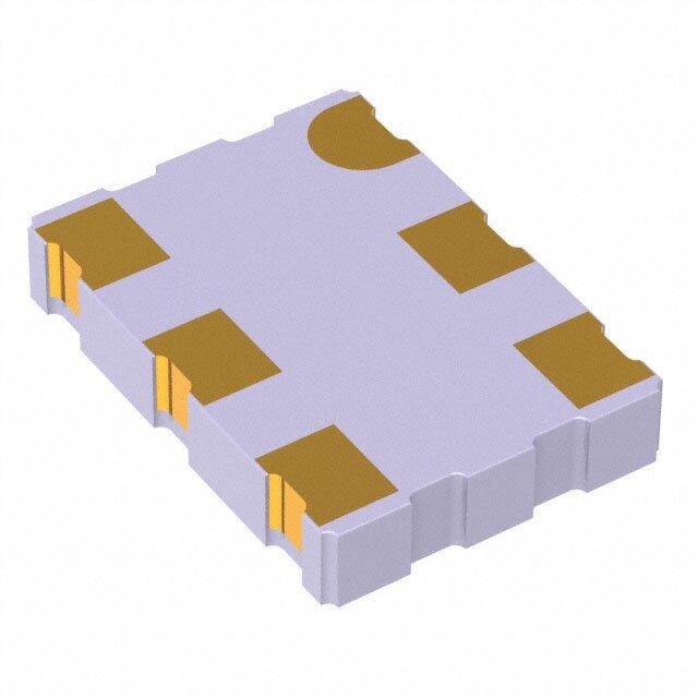
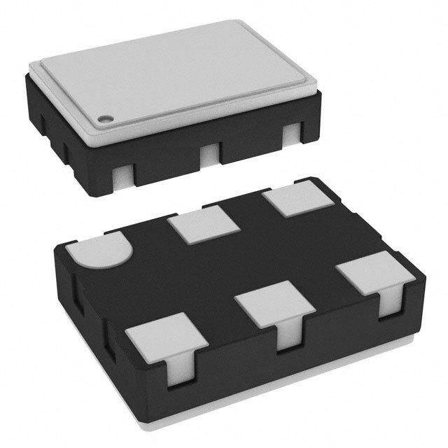
| 供应商器件封装 | TSOT-23-6 |
| 其它名称 | LTC6992IS6-4#TRMPBFCT |
| 包装 | 剪切带 (CT) |
| 安装类型 | 表面贴装 |
| 封装/外壳 | SOT-23-6 细型,TSOT-23-6 |
| 工作温度 | -40°C ~ 85°C |
| 标准包装 | 1 |
| 特色产品 | http://www.digikey.com/cn/zh/ph/LT/LTC6992.htmlhttp://www.digikey.com/product-highlights/cn/zh/linear-technology-timerblox/1523 |
| 电压-电源 | 2.25 V ~ 5.5 V |
| 电流-电源 | 365µA |
| 类型 | 振荡器 - 硅 |
| 计数 | - |
| 配用 | /product-detail/zh/DC1562B-C/DC1562B-C-ND/4864046/product-detail/zh/DC1562B-D/DC1562B-D-ND/4808974/product-detail/zh/DC1562B-E/DC1562B-E-ND/3821037/product-detail/zh/DC1562A-F/DC1562A-F-ND/3316747/product-detail/zh/DC1562A-D/DC1562A-D-ND/3316745/product-detail/zh/DC1562A-C/DC1562A-C-ND/3316739 |
| 频率 | 3.81Hz ~ 1MHz |


- 商务部:美国ITC正式对集成电路等产品启动337调查
- 曝三星4nm工艺存在良率问题 高通将骁龙8 Gen1或转产台积电
- 太阳诱电将投资9.5亿元在常州建新厂生产MLCC 预计2023年完工
- 英特尔发布欧洲新工厂建设计划 深化IDM 2.0 战略
- 台积电先进制程称霸业界 有大客户加持明年业绩稳了
- 达到5530亿美元!SIA预计今年全球半导体销售额将创下新高
- 英特尔拟将自动驾驶子公司Mobileye上市 估值或超500亿美元
- 三星加码芯片和SET,合并消费电子和移动部门,撤换高东真等 CEO
- 三星电子宣布重大人事变动 还合并消费电子和移动部门
- 海关总署:前11个月进口集成电路产品价值2.52万亿元 增长14.8%


PDF Datasheet 数据手册内容提取
LTC6992-1/LTC6992-2/ LTC6992-3/LTC6992-4 TimerBlox: Voltage-Controlled Pulse Width Modulator (PWM) FeaTures DescripTion n Pulse Width Modulation (PWM) Controlled by The LTC®6992 is a silicon oscillator with an easy-to-use Simple 0V to 1V Analog Input analog voltage-controlled pulse width modulation (PWM) n Four Available Options Define Duty Cycle Limits capability. The LTC6992 is part of the TimerBlox® family – Minimum Duty Cycle at 0% or 5% of versatile silicon timing devices. – Maximum Duty Cycle at 95% or 100% A single resistor, R , programs the LTC6992’s inter- SET n Frequency Range: 3.81Hz to 1MHz nal master oscillator frequency. The output frequency n Configured with 1 to 3 Resistors is determined by this master oscillator and an internal n <1.7% Maximum Frequency Error frequency divider, N , programmable to eight settings DIV n PWM Duty Cycle Error <3.7% Maximum from 1 to 16384. n Frequency Modulation (VCO) Capability n 2.25V to 5.5V Single Supply Operation 1MHz 50kΩ f = • ,N = 1,4,16 …16384 n 115μA Supply Current at 100kHz OUT N R DIV DIV SET n 500μs Start-Up Time Applying a voltage between 0V and 1V on the MOD pin n CMOS Output Driver Sources/Sinks 20mA sets the duty cycle. n –55°C to 125°C Operating Temperature Range n Available in Low Profile (1mm) SOT-23 (ThinSOT™) The four versions differ in their minimum/maximum duty and 2mm × 3mm DFN cycle. Note that a minimum duty cycle limit of 0% or maximum duty cycle limit of 100% allows oscillations to applicaTions stop at the extreme duty cycle settings. DEVICE NAME PWM DUTY CYCLE RANGE n PWM Servo Loops LTC6992-1 0% to 100% n Heater Control LTC6992-2 5% to 95% n LED Dimming Control LTC6992-3 0% to 95% n High Vibration, High Acceleration Environments LTC6992-4 5% to 100% n Portable and Battery-Powered Equipment For easy configuration of the LTC6992, download the L, LT, LTC and LTM, Linear Technology, TimerBlox and the Linear logo are registered trademarks and ThinSOT is a trademark of Linear Technology Corporation. All other trademarks TimerBlox Designer tool at www.linear.com/timerblox. are the property of their respective owners. Typical applicaTion 1MHz Pulse Width Modulator ANALOG PWM DUTY CYCLE MOD OUT MOD CONTROL 0.5V/DIV (0V TO 1V) LTC6992 3.3V GND V+ C1 OUT 0.1µF 1V/DIV SET DIV RSET 6992 TA01a 50k 2µs/DIV 6992 TA01b 69921234fc 1
LTC6992-1/LTC6992-2/ LTC6992-3/LTC6992-4 absoluTe MaxiMuM raTings (Note 1) Supply Voltage (V+) to GND .........…………………….6V Specified Temperature Range (Note 3) Maximum Voltage On Any Pin LTC6992C ................................................0°C to 70°C .............................(GND – 0.3V) ≤ V ≤ (V+ + 0.3V) LTC6992I .............................................–40°C to 85°C PIN Operating Temperature Range (Note 2) LTC6992H ..........................................–40°C to 125°C LTC6992C ............................................–40°C to 85°C LTC6992MP .......................................–55°C to 125°C LTC6992I .............................................–40°C to 85°C Junction Temperature ..........................................150°C LTC6992H ..........................................–40°C to 125°C Storage Temperature Range ..................–65°C to 150°C LTC6992MP .......................................–55°C to 125°C Lead Temperature (Soldering, 10 sec) S6 Package .......................................................300°C pin conFiguraTion TOP VIEW TOP VIEW V+ 1 6 OUT MOD 1 6 OUT 7 DIV 2 GND 5 GND GND 2 5 V+ SET 3 4 MOD SET 3 4 DIV S6 PACKAGE DCB PACKAGE 6-LEAD PLASTIC TSOT-23 6-LEAD (2mm × 3mm) PLASTIC DFN TJMAX = 150°C, θJA = 64°C/W, θJC = 10.6°C/W TJMAX = 150°C, θJA = 192°C/W, θJC = 51°C/W EXPOSED PAD (PIN 7) IS GND, PCB CONNECTION IS OPTIONAL orDer inForMaTion Lead Free Finish TAPE AND REEL (MINI) TAPE AND REEL PART MARKING* PACKAGE DESCRIPTION SPECIFIED TEMPERATURE RANGE LTC6992CDCB-1#TRMPBF LTC6992CDCB-1#TRPBF LDXC 6-Lead (2mm × 3mm) Plastic DFN 0°C to 70°C LTC6992IDCB-1#TRMPBF LTC6992IDCB-1#TRPBF LDXC 6-Lead (2mm × 3mm) Plastic DFN –40°C to 85°C LTC6992HDCB-1#TRMPBF LTC6992HDCB-1#TRPBF LDXC 6-Lead (2mm × 3mm) Plastic DFN –40°C to 125°C LTC6992CS6-1#TRMPBF LTC6992CS6-1#TRPBF LTDXB 6-Lead Plastic TSOT-23 0°C to 70°C LTC6992IS6-1#TRMPBF LTC6992IS6-1#TRPBF LTDXB 6-Lead Plastic TSOT-23 –40°C to 85°C LTC6992HS6-1#TRMPBF LTC6992HS6-1#TRPBF LTDXB 6-Lead Plastic TSOT-23 –40°C to 125°C LTC6992CDCB-2#TRMPBF LTC6992CDCB-2#TRPBF LDXF 6-Lead (2mm × 3mm) Plastic DFN 0°C to 70°C LTC6992IDCB-2#TRMPBF LTC6992IDCB-2#TRPBF LDXF 6-Lead (2mm × 3mm) Plastic DFN –40°C to 85°C LTC6992HDCB-2#TRMPBF LTC6992HDCB-2#TRPBF LDXF 6-Lead (2mm × 3mm) Plastic DFN –40°C to 125°C LTC6992CS6-2#TRMPBF LTC6992CS6-2#TRPBF LTDXD 6-Lead Plastic TSOT-23 0°C to 70°C LTC6992IS6-2#TRMPBF LTC6992IS6-2#TRPBF LTDXD 6-Lead Plastic TSOT-23 –40°C to 85°C LTC6992HS6-2#TRMPBF LTC6992HS6-2#TRPBF LTDXD 6-Lead Plastic TSOT-23 –40°C to 125°C LTC6992CDCB-3#TRMPBF LTC6992CDCB-3#TRPBF LFCP 6-Lead (2mm × 3mm) Plastic DFN 0°C to 70°C LTC6992IDCB-3#TRMPBF LTC6992IDCB-3#TRPBF LFCP 6-Lead (2mm × 3mm) Plastic DFN –40°C to 85°C LTC6992HDCB-3#TRMPBF LTC6992HDCB-3#TRPBF LFCP 6-Lead (2mm × 3mm) Plastic DFN –40°C to 125°C LTC6992CS6-3#TRMPBF LTC6992CS6-3#TRPBF LTFCQ 6-Lead Plastic TSOT-23 0°C to 70°C LTC6992IS6-3#TRMPBF LTC6992IS6-3#TRPBF LTFCQ 6-Lead Plastic TSOT-23 –40°C to 85°C LTC6992HS6-3#TRMPBF LTC6992HS6-3#TRPBF LTFCQ 6-Lead Plastic TSOT-23 –40°C to 125°C 69921234fc 2
LTC6992-1/LTC6992-2/ LTC6992-3/LTC6992-4 orDer inForMaTion Lead Free Finish TAPE AND REEL (MINI) TAPE AND REEL PART MARKING* PACKAGE DESCRIPTION SPECIFIED TEMPERATURE RANGE LTC6992CDCB-4#TRMPBF LTC6992CDCB-4#TRPBF LFCR 6-Lead (2mm × 3mm) Plastic DFN 0°C to 70°C LTC6992IDCB-4#TRMPBF LTC6992IDCB-4#TRPBF LFCR 6-Lead (2mm × 3mm) Plastic DFN –40°C to 85°C LTC6992HDCB-4#TRMPBF LTC6992HDCB-4#TRPBF LFCR 6-Lead (2mm × 3mm) Plastic DFN –40°C to 125°C LTC6992CS6-4#TRMPBF LTC6992CS6-4#TRPBF LTFCS 6-Lead Plastic TSOT-23 0°C to 70°C LTC6992IS6-4#TRMPBF LTC6992IS6-4#TRPBF LTFCS 6-Lead Plastic TSOT-23 –40°C to 85°C LTC6992HS6-4#TRMPBF LTC6992HS6-4#TRPBF LTFCS 6-Lead Plastic TSOT-23 –40°C to 125°C LTC6992MPS6-1#TRMPBF LTC6992MPS6-1#TRPBF LTDXB 6-Lead Plastic TSOT-23 –55°C to 125°C LTC6992MPS6-2#TRMPBF LTC6992MPS6-2#TRPBF LTDXD 6-Lead Plastic TSOT-23 –55°C to 125°C LTC6992MPS6-3#TRMPBF LTC6992MPS6-3#TRPBF LTFCQ 6-Lead Plastic TSOT-23 –55°C to 125°C LTC6992MPS6-4#TRMPBF LTC6992MPS6-4#TRPBF LTFCS 6-Lead Plastic TSOT-23 –55°C to 125°C TRM = 500 pieces. *Temperature grades are identified by a label on the shipping container. Consult LTC Marketing for parts specified with wider operating temperature ranges. Consult LTC Marketing for information on lead based finish parts. For more information on lead free part marking, go to: http://www.linear.com/leadfree/ For more information on tape and reel specifications, go to: http://www.linear.com/tapeandreel/ elecTrical characTerisTics The l denotes the specifications which apply over the full operating temperature range, otherwise specifications are at T = 25°C. Test conditions are V+ = 2.25V to 5.5V, V = 0V to V , A MOD SET DIVCODE = 0 to 15 (N = 1 to 16,384), R = 50k to 800k, R = 5k, C = 5pF unless otherwise noted. DIV SET LOAD LOAD SYMBOL PARAMETER CONDITIONS MIN TYP MAX UNITS Oscillation Frequency f Output Frequency 3.81 1000000 Hz OUT ∆fOUT Frequency Accuracy (Note 4) 3.81Hz ≤ fOUT ≤ 1MHz ±0.8 ±1.7 % l ±2.4 % ∆fOUT/∆T Frequency Drift Over Temperature l ±0.005 %/°C ∆fOUT/∆V+ Frequency Drift Over Supply V+ = 4.5V to 5.5V l 0.25 0.65 %/V V+ = 2.25V to 4.5V l 0.08 0.18 %/V Long-Term Frequency Stability (Note 10) 90 ppm/√kHr Period Jitter (Note 9) N = 1 1.2 % DIV P-P N = 4 0.4 % DIV P-P 0.07 % RMS N = 16 0.15 % DIV P-P 0.022 % RMS Pulse Width Modulation ∆D PWM Duty Cycle Accuracy VMOD = 0.2•VSET to 0.8•VSET ±3.0 ±3.7 % V = 0.2•V to 0.8•V l ±4.5 % MOD SET SET V < 0.2•V or V > 0.8•V l ±4.9 % MOD SET MOD SET D Maximum Duty Cycle Limit LTC6992-1/LTC6992-4, POL = 0, V = 1V l 100 % MAX MOD LTC6992-2/LTC6992-3, POL = 0, V = 1V l 90.5 95 99 % MOD D Minimum Duty Cycle Limit LTC6992-1/LTC6992-3, POL = 0, V = 0V l 0 % MIN MOD LTC6992-2/LTC6992-4, POL = 0, V = 0V l 1 5 9.5 % MOD t Duty Cycle Settling Time (Note 6) t = t /N 8•t µs S,PWM MASTER OUT DIV MASTER 69921234fc 3
LTC6992-1/LTC6992-2/ LTC6992-3/LTC6992-4 elecTrical characTerisTics The l denotes the specifications which apply over the full operating temperature range, otherwise specifications are at T = 25°C. Test conditions are V+ = 2.25V to 5.5V, V = 0V to V , A MOD SET DIVCODE = 0 to 15 (N = 1 to 16,384), R = 50k to 800k, R = 5k, C = 5pF unless otherwise noted. DIV SET LOAD LOAD SYMBOL PARAMETER CONDITIONS MIN TYP MAX UNITS Power Supply V+ Operating Supply Voltage Range l 2.25 5.5 V Power-On Reset Voltage l 1.95 V I Supply Current R = ∞, R = 50k, V+ = 5.5V l 365 450 µA S L SET NDIV = 1 V+ = 2.25V l 225 285 µA R = ∞, R = 50k, V+ = 5.5V l 350 420 µA L SET NDIV = 4 V+ = 2.25V l 225 280 µA R = ∞, R = 50k, V+ = 5.5V l 325 390 µA L SET NDIV ≥ 16 V+ = 2.25V l 215 265 µA R = ∞, R = 800k, V+ = 5.5V l 120 170 µA L SET NDIV = 1 to 16,384 V+ = 2.25V l 105 150 µA Analog Inputs V Voltage at SET Pin l 0.97 1.00 1.03 V SET ∆V /∆T V Drift Over Temperature l ±75 µV/°C SET SET R Frequency-Setting Resistor l 50 800 kΩ SET MOD Pin Input Capacitance 2.5 pF MOD Pin Input Current l ±10 nA V V Voltage for Maximum LTC6992-1/LTC6992-4, POL = 0, D = 100% l 0.90•V 0.936•V V MOD,HI MOD SET SET Duty Cycle LTC6992-2/LTC6992-3, POL = 0, D = 95% 0.86•V V SET V V Voltage for Minimum LTC6992-1/LTC6992-3, POL = 0, D = 0% l 0.064•V 0.10•V V MOD,LO MOD SET SET Duty Cycle LTC6992-2/LTC6992-4, POL = 0, D = 5% 0.14•V V SET V DIV Pin Voltage l 0 V+ V DIV ∆V /∆V+ DIV Pin Valid Code Range (Note 5) Deviation from Ideal l ±1.5 % DIV V /V+ = (DIVCODE + 0.5)/16 DIV DIV Pin Input Current l ±10nA Digital Output I Output Current V+ = 2.7V to 5.5V ±20 mA OUT(MAX) V High Level Output Voltage (Note 7) V+ = 5.5V I = –1mA l 5.45 5.48 V OH OUT I = –16mA l 4.84 5.15 V OUT V+ = 3.3V I = –1mA l 3.24 3.27 V OUT I = –10mA l 2.75 2.99 V OUT V+ = 2.25V I = –1mA l 2.17 2.21 V OUT I = -8mA l 1.58 1.88 V OUT V Low Level Output Voltage (Note 7) V+ = 5.5V I = 1mA l 0.02 0.04 V OL OUT I = 16mA l 0.26 0.54 V OUT V+ = 3.3V I = 1mA l 0.03 0.05 V OUT I = 10mA l 0.22 0.46 V OUT V+ = 2.25V I = 1mA l 0.03 0.07 V OUT I = 8mA l 0.26 0.54 V OUT t Output Rise Time (Note 8) V+ = 5.5V, R = ∞ 1.1 ns r LOAD V+ = 3.3V, R = ∞ 1.7 ns LOAD V+ = 2.25V, R = ∞ 2.7 ns LOAD t Output Fall Time (Note 8) V+ = 5.5V, R = ∞ 1.0 ns f LOAD V+ = 3.3V, R = ∞ 1.6 ns LOAD V+ = 2.25V, R = ∞ 2.4 ns LOAD 69921234fc 4
LTC6992-1/LTC6992-2/ LTC6992-3/LTC6992-4 elecTrical characTerisTics Note 1: Stresses beyond those listed under Absolute Maximum Ratings Note 7: To conform to the Logic IC Standard, current out of a pin is may cause permanent damage to the device. Exposure to any Absolute arbitrarily given a negative value. Maximum Rating condition for extended periods may affect device Note 8: Output rise and fall times are measured between the 10% and the reliability and lifetime. 90% power supply levels with 5pF output load. These specifications are Note 2: The LTC6992C is guaranteed functional over the operating based on characterization. temperature range of –40°C to 85°C. Note 9: Jitter is the ratio of the peak-to-peak deviation of the period to the Note 3: The LTC6992C is guaranteed to meet specified performance from mean of the period. This specification is based on characterization and is 0°C to 70°C. The LTC6992C is designed, characterized and expected to not 100% tested. meet specified performance from –40°C to 85°C but it is not tested or Note 10: Long-term drift of silicon oscillators is primarily due to the QA sampled at these temperatures. The LTC6992I is guaranteed to meet movement of ions and impurities within the silicon and is tested at 30°C specified performance from –40°C to 85°C. The LTC6992H is guaranteed under otherwise nominal operating conditions. Long-term drift is specified to meet specified performance from –40°C to 125°C. The LTC6992MP is as ppm/√kHr due to the typically nonlinear nature of the drift. To calculate guaranteed to meet specified performance from –55°C to 125°C. drift for a set time period, translate that time into thousands of hours, take Note 4: Frequency accuracy is defined as the deviation from the fOUT the square root and multiply by the typical drift number. For instance, a equation, assuming R is used to program the frequency. SET year is 8.77kHr and would yield a drift of 266ppm at 90ppm/√kHr. Drift Note 5: See Operation section, Table 1 and Figure 2 for a full explanation without power applied to the device may be approximated as 1/10th of the of how the DIV pin voltage selects the value of DIVCODE. drift with power, or 9ppm/√kHr for a 90ppm/√kHr device. Note 6: Duty cycle settling time is the amount of time required for the output to settle within ±1% of the final duty cycle after a ±10% change in the setting (±80mV step in V ). MOD Typical perForMance characTerisTics V+ = 3.3V, R = 200k, and T = 25°C, unless SET A otherwise noted. Frequency Error vs Temperature Frequency Error vs Temperature Frequency Error vs Temperature 3 3 3 GUARANTEED MAX OVER TEMPERATURE GUARANTEED MAX OVER TEMPERATURE GUARANTEED MAX OVER TEMPERATURE 2 RSET = 50k 2 RSET = 200k 2 RSET = 800k 3 PARTS 3 PARTS 3 PARTS 1 1 1 %) %) %) OR ( 0 OR ( 0 OR ( 0 R R R R R R E E E –1 –1 –1 –2 –2 –2 GUARANTEED MIN OVER TEMPERATURE GUARANTEED MIN OVER TEMPERATURE GUARANTEED MIN OVER TEMPERATURE –3 –3 –3 –50 –25 0 25 50 75 100 125 –50 –25 0 25 50 75 100 125 –50 –25 0 25 50 75 100 125 TEMPERATURE (°C) TEMPERATURE (°C) TEMPERATURE (°C) 6992 G01 6992 G02 6992 G03 69921234fc 5
LTC6992-1/LTC6992-2/ LTC6992-3/LTC6992-4 Typical perForMance characTerisTics V+ = 3.3V, R = 200k, and T = 25°C, unless SET A otherwise noted. Frequency Error vs R Frequency Drift vs Supply Voltage Typical V Distribution SET SET 3 0.5 250 GUARANTEED MAX OVER TEMPERATURE 2 LOTS 0.4 DFN AND SOT-23 2 3 PARTS 0.3 200 1274 UNITS %) 1 %) 00..21 RSET = 50k UNITS 150 ERROR ( 0 DRIFT (–0.01 MBER OF 100 –1 U –0.2 RSET = 200k RSET = 800k N –0.3 50 –2 –0.4 GUARANTEED MIN OVER TEMPERATURE REFERENCED TO V+ = 4.5V –3 –0.5 0 50 100 200 400 800 2 3 4 5 6 0.98 0.988 0.996 1.004 1.012 1.02 RSET (k) SUPPLY VOLTAGE (V) VSET (V) 6992 G04 6992 G05 6992 G06 V Drift vs I V Drift vs Supply V vs Temperature SET SET SET SET 1.0 1.0 1.020 3 PARTS 0.8 0.8 1.015 0.6 0.6 1.010 0.4 0.4 mV) 0.2 mV) 0.2 V) 1.005 V (SET–0.02 DRIFT (–0.02 V (SET10..090905 –0.4 –0.4 0.990 –0.6 –0.6 –0.8 –0.8 0.985 REFERENCED TO ISET = 10µA REFERENCED TO V+ = 4V –1.0 –1.0 0.980 0 5 10 15 20 2 3 4 5 6 –50 –25 0 25 50 75 100 125 ISET (µA) SUPPLY (V) TEMPERATURE (°C) 6992 G07 6992 G08 6992 G09 N = 1 Duty Cycle Error vs R N = 1 Duty Cycle Error vs R N = 1 Duty Cycle Error vs R DIV SET DIV SET DIV SET 5 5 5 VMOD/VSET = 0.2 (12.5%) VMOD/VSET = 0.5 (50%) VMOD/VSET = 0.8 (87.5%) 4 DIVCODE = 0 4 DIVCODE = 0 4 DIVCODE = 0 3 PARTS 3 PARTS 3 PARTS 3 3 3 2 2 2 %) 1 %) 1 %) 1 OR ( 0 OR ( 0 OR ( 0 R R R ER –1 ER –1 ER –1 –2 –2 –2 –3 –3 –3 –4 –4 –4 –5 –5 –5 50 100 200 400 800 50 100 200 400 800 50 100 200 400 800 RSET (k) RSET (k) RSET (k) 6992 G10 6992 G11 6992 G12 69921234fc 6
LTC6992-1/LTC6992-2/ LTC6992-3/LTC6992-4 Typical perForMance characTerisTics V+ = 3.3V, R = 200k, and T = 25°C, unless SET A otherwise noted. N > 1 Duty Cycle Error vs R N > 1 Duty Cycle Error vs R N > 1 Duty Cycle Error vs R DIV SET DIV SET DIV SET 5 5 5 VMOD/VSET = 0.2 (12.5%) VMOD/VSET = 0.5 (50%) VMOD/VSET = 0.8 (87.5%) 4 DIVCODE = 4 4 DIVCODE = 4 4 DIVCODE = 4 3 PARTS 3 PARTS 3 PARTS 3 3 3 2 2 2 %) 1 %) 1 %) 1 OR ( 0 OR ( 0 OR ( 0 R R R ER –1 ER –1 ER –1 –2 –2 –2 –3 –3 –3 –4 –4 –4 –5 –5 –5 50 100 200 400 800 50 100 200 400 800 50 100 200 400 800 RSET (k) RSET (k) RSET (k) 6992 G13 6992 G14 6992 G15 NDIV = 1 Duty Cycle Clamps NDIV = 1 Duty Cycle Error vs RSET NDIV > 1 Duty Cycle Error vs RSET vs Temperature 97 97 5 DIVCODE = 0 DIVCODE = 4 96 3 PARTS 96 3 PARTS 4 GUARANTEED MAX 95 95 3 VMOD/VSET = 0.2 (12.5%) 94 LTC6992-2/LTC6992-3 94 DIVCODE = 0 2 3 PARTS 93 VMOD = VSET 93 LTC6992-2/LTC6992-3 %) 92 %) 92 VMOD = VSET %) 1 OR ( OR ( OR ( 0 R R R ER 8 ER 8 ER –1 76 LVTMCO6D9 9=2 V-2S/ELTTC6992-4 76 LVTMCO6D9 9=2 V-2S/ELTTC6992-4 –2 –3 5 5 4 4 –4 GUARANTEED MIN 3 3 –5 50 100 200 400 800 50 100 200 400 800 –50 –25 0 25 50 75 100 125 RSET (k) RSET (k) TEMPERATURE (°C) 6992 G16 6992 G17 6992 G18 NDIV = 1 Duty Cycle Error NDIV = 1 Duty Cycle Error NDIV > 1 Duty Cycle Error vs Temperature vs Temperature vs Temperature 5 5 5 4 GUARANTEED MAX 4 GUARANTEED MAX 4 GUARANTEED MAX 3 VDMIVOCDO/VDSEE =T =0 0.5 (50%) 3 DVMIVOCDO/VDSEE =T =0 0.8 (87.5%) 3 VDMIVOCDO/VDSEE =T =4 0.2 (12.5%) 2 3 PARTS 2 3 PARTS 2 3 PARTS %) 1 %) 1 %) 1 OR ( 0 OR ( 0 OR ( 0 R R R ER –1 ER –1 ER –1 –2 –2 –2 –3 –3 –3 –4 GUARANTEED MIN –4 GUARANTEED MIN –4 GUARANTEED MIN –5 –5 –5 –50 –25 0 25 50 75 100 125 –50 –25 0 25 50 75 100 125 –50 –25 0 25 50 75 100 125 TEMPERATURE (°C) TEMPERATURE (°C) TEMPERATURE (°C) 6992 G19 6992 G20 6992 G21 69921234fc 7
LTC6992-1/LTC6992-2/ LTC6992-3/LTC6992-4 Typical perForMance characTerisTics V+ = 3.3V, R = 200k, and T = 25°C, unless SET A otherwise noted. NDIV > 1 Duty Cycle Error NDIV > 1 Duty Cycle Error NDIV = 1 Duty Cycle Clamps vs Temperature vs Temperature vs Temperature 5 5 97 DIVCODE = 0 4 GUARANTEED MAX 4 GUARANTEED MAX 96 3 PARTS 3 VMOD/VSET = 0.5 (50%) 3 VMOD/VSET = 0.8 (87.5%) 95 DIVCODE = 4 DIVCODE = 4 94 2 3 PARTS 2 3 PARTS LTC6992-2/LTC6992-3 93 VMOD = VSET %) 1 %) 1 %) 92 OR ( 0 OR ( 0 OR ( ERR –1 ERR –1 ERR 8 7 –2 –2 LTC6992-2/LTC6992-4 –3 –3 6 VMOD = GND 5 –4 GUARANTEED MIN –4 GUARANTEED MIN 4 –5 –5 3 –50 –25 0 25 50 75 100 125 –50 –25 0 25 50 75 100 125 –50 –25 0 25 50 75 100 125 TEMPERATURE (°C) TEMPERATURE (°C) TEMPERATURE (°C) 6992 G22 6992 G23 6992 G24 N > 1 Duty Cycle Clamps DIV vs Temperature Duty Cycle Error vs DIVCODE Duty Cycle Error vs DIVCODE 97 5 5 96 D3 IPVACROTDSE = 4 4 V3 MPOADR/TVSSET = 0.2 (12.5%) 4 V3 MPOADR/TVSSET = 0.5 (50%) 95 3 3 94 2 2 %) 93 LTC6992-2/LTC6992-3 E ( 92 VMOD = VSET %) 1 %) 1 DUTY CYCL 87 LTC6992-2/LTC6992-4 ERROR ( –10 ERROR ( –10 6 VMOD = GND –2 –2 –3 –3 5 4 –4 –4 3 –5 –5 –50 –25 0 25 50 75 100 125 0 2 4 6 8 10 12 14 0 2 4 6 8 10 12 14 TEMPERATURE (°C) DIVCODE DIVCODE 6992 G25 6992 G26 6992 G27 Duty Cycle Error vs DIVCODE NDIV = 1 Duty Cycle vs VMOD/ VSET NDIV > 1 Duty Cycle vs VMOD/ VSET 5 100 100 4 V3 MPOADR/TVSSET = 0.8 (87.5%) 90 D3 IPVACROTDSE = 0 LLTTCC66999922--14/ 90 D3 IPVACROTDSE = 4 LLTTCC66999922--14/ 3 80 80 LTC6992-2/ LTC6992-2/ 2 %) 70 LTC6992-3 %) 70 LTC6992-3 ERROR (%) ––1102 DUTY CYCLE ( 46530000 LLTTCC66999922--24/ DUTY CYCLE ( 46530000 LLTTCC66999922--24/ –3 20 20 –4 10 10 LTC6992-1/LTC6992-3 LTC6992-1/LTC6992-3 –5 0 0 0 2 4 6 8 10 12 14 0 0.2 0.4 0.6 0.8 1 0 0.2 0.4 0.6 0.8 1 DIVCODE VMOD/VSET (V/V) VMOD/VSET (V/V) 6992 G28 6992 G29 6992 G30 69921234fc 8
LTC6992-1/LTC6992-2/ LTC6992-3/LTC6992-4 Typical perForMance characTerisTics V+ = 3.3V, R = 200k, and T = 25°C, unless SET A otherwise noted. N > 1 Duty Cycle vs V /V N = 1 Duty Cycle Error vs Ideal N > 1 Duty Cycle Error vs Ideal DIV MOD SET DIV DIV 100 5 5 DIVCODE = 0 DIVCODE = 4 LTC6992-1/LTC6992-3 90 4 3 PARTS 4 3 PARTS 80 3 3 70 LTC6992-2/ 2 2 UTY CYCLE (%) 465000 LTC6992-4 LTC6992-2/ ERROR (%) –011 PART B PART APART C ERROR (%) –011 PART B PART C D 30 LTC6992-3 –2 –2 PART A 20 –3 –3 10 DIVCODE = 11 LTC6992-1/ –4 –4 3 PARTS LTC6992-4 0 –5 –5 0 0.2 0.4 0.6 0.8 1 0 25 50 75 100 0 25 50 75 100 VMOD/VSET (V/V) IDEAL DUTY CYCLE (%) IDEAL DUTY CYCLE (%) 6992 G31 6992 G32 6992 G33 N > 1 Duty Cycle Error vs Ideal Linearity Near 100% Duty Cycle Linearity Near 95% Duty Cycle DIV 5 100 100 DIVCODE = 11 DIVCODE = 4 DIVCODE = 4 4 3 PARTS 99 LTC6992-1/LTC6992-4 99 LTC6992-2/LTC6992-3 98 3 PARTS 98 3 PARTS 3 PART A 97 97 2 PART C %) 96 %) 96 %) 1 E ( 95 E ( 95 ERROR ( –01 PART B UTY CYCL 9943 UTY CYCL 9943 D 92 D 92 –2 91 91 –3 90 90 –4 89 89 –5 88 88 0 25 50 75 100 0.804 0.836 0.868 0.9 0.804 0.836 0.868 0.9 IDEAL DUTY CYCLE (%) VMOD/VSET (V/V) VMOD/VSET (V/V) 6992 G34 6992 G35 6992 G36 Linearity Near 67% Duty Cycle Linearity Near 0% Duty Cycle Linearity Near 5% Duty Cycle 72 12 12 DIVCODE = 4 DIVCODE = 4 DIVCODE = 4 71 3 PARTS 11 LTC6992-1/LTC6992-3 11 LTC6992-2/LTC6992-4 10 3 PARTS 10 3 PARTS 70 9 9 69 %) %) 8 %) 8 E ( 68 E ( 7 E ( 7 L L L YC 67 YC 6 YC 6 C C C TY 66 TY 5 TY 5 U U U D D 4 D 4 65 3 3 64 2 2 63 1 1 62 0 0 0.596 0.612 0.628 0.644 0.66 0.676 0.084 0.116 0.148 0.18 0.084 0.116 0.148 0.18 VMOD/VSET (V/V) VMOD/VSET (V/V) VMOD/VSET (V/V) 6992 G37 6992 G38 6992 G39 69921234fc 9
LTC6992-1/LTC6992-2/ LTC6992-3/LTC6992-4 Typical perForMance characTerisTics V+ = 3.3V, R = 200k, and T = 25°C, unless SET A otherwise noted. N > 1 Duty Cycle Drift DIV Linearity Near 31% Duty Cycle NDIV = 1 Duty Cycle Drift vs Supply vs Supply 36 0.5 0.5 DIVCODE = 4 DIVCODE = 0 DIVCODE = 4 35 3 PARTS 0.4 0.4 34 0.3 0.3 5% CLAMP E (%) 3332 %) 00..21 5% CLAMP 95% CLAMP %) 00..21 VMOD/VS9E5T %= 0C.L2AMP TY CYCL 3310 DRIFT (–0.01 DRIFT (–0.01 DU VMOD/VSET = 0.8 VMOD/VSET = 0.5 29 –0.2 –0.2 VMOD/VSET = 0.2 VMOD/VSET = 0.8 28 –0.3 VMOD/VSET = 0.5 –0.3 27 –0.4 –0.4 REFERENCED TO V+ = 4V REFERENCED TO V+ = 4V 26 –0.5 –0.5 0.308 0.324 0.34 0.356 0.372 0.388 2 3 4 5 6 2 3 4 5 6 VMOD/VSET (V/V) SUPPLY (V) SUPPLY (V) 6992 G40 6992 G41 6992 G42 Supply Current vs V Supply Current vs Supply Voltage Supply Current vs Temperature MOD 400 400 400 LTC6992-2 350 350 RSET = 50k, ÷1 350 5.0V, RSET = 50k, ÷1 NT (µA) 300 RSET = 50k, ÷1 NT (µA) 300 RSET = 50k, ÷4 NT (µA)300 5.0V, RSET = 50k, ÷16 RRE 250 RRE 250 RSET = 50k, ÷16 RRE250 2.5V, RSET = 50k, ÷1 CU RSET = 50k, ÷16 CU CU PLY 200 PLY 200 RSET = 100k, ÷1 PLY 200 UP 150 RSET = 100k, ÷4 UP 150 UP150 R S R S R S 5.0V, RSET = 800k, ÷1 OWE 100 RSET = 800k, ÷1 OWE 100 RSET = 800k, ÷1 OWE100 2.5V, RSET = 800k, ÷1 P P P 50 50 50 0 0 0 0 0.2 0.4 0.6 0.8 1 2 3 4 5 6 –50 –25 0 25 50 75 100 125 VMOD (V) SUPPLY VOLTAGE (V) TEMPERATURE (°C) 6992 G43 6992 G44 6992 G45 Jitter vs Frequency Supply Current vs Frequency, 5V Supply Current vs Frequency, 2.5V 2.0 PEAK-TO-PEAK PERIOD 400 V+ = 5V 400 V+ = 2.5V 1.8 DEVIATION MEASURED 350 350 JITTER (%)P-P111100......462086 OVMVEORD/ 3V0SsE TI N=T 0E.R5VAL÷S÷41, ,V V+ += = 5 2V.5÷V1, V+ = 5V R SUPPLY CURRENT (µA)232150050000 ÷16,384 ÷4÷1 R SUPPLY CURRENT (µA)232150050000 ÷16,384 ÷4÷1 ÷4, V+ = 2.5V WE100 WE100 0.4 O O ÷16 P P 0.2 ÷64 50 50 0 0 0 0.01 0.1 1 10 100 1000 0.001 0.01 0.1 1 10 100 1000 0.001 0.01 0.1 1 10 100 1000 FREQUENCY (kHz) FREQUENCY (kHz) FREQUENCY (kHz) 6992 G46 6992 G47 6992 G48 69921234fc 10
LTC6992-1/LTC6992-2/ LTC6992-3/LTC6992-4 Typical perForMance characTerisTics V+ = 3.3V, R = 200k, and T = 25°C, unless SET A otherwise noted. Typical Frequency Error vs Output Resistance Rise and Fall Time Time (Long-Term Drift) vs Supply Voltage vs Supply Voltage 200 50 3.0 65 UNITS CLOAD = 5pF 150 SOT-23 AND DFN PARTS 45 TA = 30°C 40 2.5 m) 100 Ω) QUENCY (pp 500 ESISTANCE ( 233550 OUTPUT SOURCING CURRENT LL TIME (ns) 12..50 tRISE DELTA FRE–1–0500 OUTPUT R 2105 OUTPUT SINKING CURRENT RISE/FA 1.0 tFALL 10 0.5 –150 5 –200 0 0 0 400 800 1200 1600 2000 2400 2800 2 3 4 5 6 2 3 4 5 6 TIME (h) SUPPLY VOLTAGE (V) SUPPLY VOLTAGE (V) 6992 G48a 6992 G50 6992 G51 Typical ISET Current Limit vs V+ Typical Start-Up, POL = 0 1000 SET PIN SHORTED TO GND 800 V+ 1V/DIV A) 600 µ I (SET400 1V/ODUIVT 500µs 200 100µs/DIV 6992 G53 V+ = 2.5V DIVCODE = 3 (÷64) 0 2 3 4 5 6 RSET = 50k SUPPLY VOLTAGE (V) VMOD = 0.3V (~25% DUTY CYCLE) 6992 G52 Typical Start-Up, POL = 1 125kHz Full Modulation LTC6992-1 VMOD 0.5V/DIV V+ 1V/DIV OUT OUT 500µs 1V/DIV 1V/DIV 100µs/DIV 6992 G54 50µs/DIV 6992 G55 V+ = 2.5V V+ = 3.3V DIVCODE = 12 (÷64, POL = 1) DIVCODE = 1 RSET = 50k RSET = 100k VMOD = 0.2V (~87.5% DUTY CYCLE) 69921234fc 11
LTC6992-1/LTC6992-2/ LTC6992-3/LTC6992-4 pin FuncTions (DCB/S6) V+ (Pin 1/Pin 5): Supply Voltage (2.25V to 5.5V). This sup- Limit the capacitance on the SET pin to less than 10pF ply should be kept free from noise and ripple. It should be to minimize jitter and ensure stability. Capacitance less bypassed directly to the GND pin with a 0.1μF capacitor. than 100pF maintains the stability of the feedback circuit regulating the V voltage. DIV (Pin 2/Pin 4): Programmable Divider and Polarity SET Input. The DIV pin voltage (V ) is internally converted DIV V+ into a 4-bit result (DIVCODE). V may be generated by DIV a resistor divider between V+ and GND. Use 1% resistors MOD OUT to ensure an accurate result. The DIV pin and resistors LTC6992 V+ should be shielded from the OUT pin or any other traces GND V+ C1 that have fast edges. Limit the capacitance on the DIV pin 0.1µF R1 to less than 100pF so that V settles quickly. The MSB of SET DIV DIV DIVCODE (POL) determines if the PWM signal is inverted RSET 6992 PF R2 before driving the output. When POL = 1 the transfer func- tion is inverted (duty cycle decreasing as V increases). MOD MOD (Pin 4/Pin 1): Pulse-Width Modulation Input. The SET (Pin 3/Pin 3): Frequency-Setting Input. The voltage voltage on the MOD pin controls the output duty cycle. The on the SET pin (V ) is regulated to 1V above GND. The SET linear control range is between 0.1•V and 0.9•V SET SET amount of current sourced from the SET pin (I ) pro- SET (approximately 100mV to 900mV). Beyond those limits, grams the master oscillator frequency. The I current SET the output will either clamp at 5% or 95%, or stop oscil- range is 1.25μA to 20μA. The output oscillation will stop lating (0% or 100% duty cycle), depending on the version. if I drops below approximately 500nA. A resistor con- SET GND (Pin 5/Pin 2): Ground. Tie to a low inductance ground nected between SET and GND is the most accurate way to plane for best performance. set the frequency. For best performance, use a precision metal or thin film resistor of 0.5% or better tolerance and OUT (Pin 6/Pin 6): Oscillator Output. The OUT pin swings 50ppm/°C or better temperature coefficient. For lower ac- from GND to V+ with an output resistance of approximately curacy applications an inexpensive 1% thick film resistor 30Ω. The duty cycle is determined by the voltage on the may be used. MOD pin. When driving an LED or other low-impedance load a series output resistor should be used to limit the source/sink current to 20mA. 69921234fc 12
LTC6992-1/LTC6992-2/ LTC6992-3/LTC6992-4 block DiagraM (S6 Package Pin Numbers Shown) V+ 5 R1DIV POL 4-BIT A/D DIGITAL 4 CONVERTER FILTER R2 OUTPUT POLARITY MASTER OSCILLATOR PULSE WIDTH MODULATOR fOSC = 1MHz • 50kΩ • VISSEETT MCLK ÷1, 4,P 1R6O, G6R4,A 2M5M6,A 1B0L2E4 ,D 4IV0I9D6E, R16384 DUTY CYCLE =VMOD(LIM) – 0.1•VSET tON 0.8•VSET OUT 6 HALT OSCILLATOR DISABLE OUTPUT tOUT IF ISET < 500nA UNTIL SETTLED VMOD(LIM) D = ttOOUNT + POR VOLTAGE LIMITER – VSET = 1V +– V1VREF VMOD 3 22 1 SET GND MOD 6992 BD ISET RSET 69921234fc 13
LTC6992-1/LTC6992-2/ LTC6992-3/LTC6992-4 operaTion The LTC6992 is built around a master oscillator with a DIVCODE 1MHz maximum frequency. The oscillator is controlled The DIV pin connects to an internal, V+ referenced 4-bit A/D by the SET pin current (I ) and voltage (V ), with a SET SET converter that determines the DIVCODE value. DIVCODE 1MHz • 50k conversion factor that is accurate to ±0.8% programs two settings on the LTC6992: under typical conditions. 1. DIVCODE determines the output frequency divider set- 1 I fMASTER = t =1MHz • 50k• VSET ting, NDIV. MASTER SET 2. DIVCODE determines the output polarity, via the POL A feedback loop maintains V at 1V ±30mV, leaving I bit. SET SET as the primary means of controlling the output frequency. V may be generated by a resistor divider between V+ DIV The simplest way to generate I is to connect a resistor SET and GND as shown in Figure 1. (R ) between SET and GND, such that I = V /R . SET SET SET SET The master oscillator equation reduces to: 1 1MHz•50k f = = MASTER t R 2.25V TO 5.5V MASTER SET V+ From this equation, it is clear that VSET drift will not affect LTC6992 R1 the output frequency when using a single program resistor DIV (R ). Error sources are limited to R tolerance and SET SET R2 the inherent frequency accuracy ∆f of the LTC6992. OUT GND R may range from 50k to 800k (equivalent to I 6992 F01 SET SET between 1.25μA and 20μA). Figure 1. Simple Technique for Setting DIVCODE The LTC6992 includes a programmable frequency divider which can further divide the frequency by 1, 4, 16, 64, 256, 1024, 4096 or 16384 before driving the OUT pin. The divider ratio N is set by a resistor divider attached DIV to the DIV pin. 1 1MHz•50k I f = = • SET OUT t N V OUT DIV SET With R in place of V /I the equation reduces to: SET SET SET 1 1MHz•50k f = = OUT t N •R OUT DIV SET 69921234fc 14
LTC6992-1/LTC6992-2/ LTC6992-3/LTC6992-4 operaTion Table 1. DIVCODE Programming DIVCODE POL N RECOMMENDED f R1 (kΩ) R2 (kΩ) V /V+ DIV OUT DIV 0 0 1 62.5kHz to 1MHz Open Short ≤0.03125 ±0.015 1 0 4 15.63kHz to 250kHz 976 102 0.09375 ±0.015 2 0 16 3.906kHz to 62.5kHz 976 182 0.15625 ±0.015 3 0 64 976.6Hz to 15.63kHz 1000 280 0.21875 ±0.015 4 0 256 244.1Hz to 3.906kHz 1000 392 0.28125 ±0.015 5 0 1024 61.04Hz to 976.6Hz 1000 523 0.34375 ±0.015 6 0 4096 15.26Hz to 244.1Hz 1000 681 0.40625 ±0.015 7 0 16384 3.815Hz to 61.04Hz 1000 887 0.46875 ±0.015 8 1 16384 3.815Hz to 61.04Hz 887 1000 0.53125 ±0.015 9 1 4096 15.26Hz to 244.1Hz 681 1000 0.59375 ±0.015 10 1 1024 61.04Hz to 976.6Hz 523 1000 0.65625 ±0.015 11 1 256 244.1Hz to 3.906kHz 392 1000 0.71875 ±0.015 12 1 64 976.6Hz to 15.63kHz 280 1000 0.78125 ±0.015 13 1 16 3.906kHz to 62.5kHz 182 976 0.84375 ±0.015 14 1 4 15.63kHz to 250kHz 102 976 0.90625 ±0.015 15 1 1 62.5kHz to 1MHz Short Open ≥0.96875 ±0.015 Table 1 offers recommended 1% resistor values that ac- column in Table 1 shows the ideal ratio of V to the DIV curately produce the correct voltage division as well as the supply voltage, which can also be calculated as: corresponding N and POL values for the recommended DIV V DIVCODE+0.5 resistor pairs. Other values may be used as long as: DIV = ±1.5% V+ 16 1. The V /V+ ratio is accurate to ±1.5% (including resis- DIV tor tolerances and temperature effects). For example, if the supply is 3.3V and the desired DIVCODE is 4, V = 0.281 • 3.3V = 928mV ± 50mV. DIV 2. The driving impedance (R1||R2) does not exceed 500kΩ. Figure 2 illustrates the information in Table 1, showing If the voltage is generated by other means (i.e. the output that N is symmetric around the DIVCODE midpoint. of a DAC) it must track the V+ supply voltage. The last DIV 1000 POL BIT = 0 POL BIT = 1 0 15 100 1 14 Hz) 10 2 13 (kOUT 1 3 4 11 12 f 5 10 0.1 6 9 0.01 7 8 0.001 0V 0.5•V+ V+ INCREASING VDIV 6992 F02 Figure 2. Frequency Range and POL Bit vs DIVCODE 69921234fc 15
LTC6992-1/LTC6992-2/ LTC6992-3/LTC6992-4 operaTion Pulse Width (Duty Cycle) Modulation Output Polarity (POL Bit) The MOD pin is a high impedance analog input providing The duty cycle equation describes a proportional transfer direct control of the output duty cycle. The duty cycle is function, where duty cycle increases as V increases. MOD proportional to the voltage applied to the MOD pin, V . The LTC6992 includes a POL bit (determined by the MOD V 1 DIVCODE as described earlier) that inverts the output Duty Cycle = D = MOD − signal. This makes the duty cycle gain negative, reducing 0.8•V 8 SET duty cycle as V increases. MOD The PWM duty cycle accuracy ∆D specifies that the above equation is valid to within ±4.5% for V between 0.2 • MOD VSET and 0.8 • VSET (12.5% to 87.5% duty cycle). POL = 0 D= VMOD −1 Since V = 1V ±30mV, the duty cycle equation may be D•tOUT 0.8•VSET 8 SET approximated by the following equation. OUT V −100mV Duty Cycle = D ≅ MOD tOUT 800mV POL = 1 TDhriev iVngM OVDM OcDo nbteryool nrdan tghea t irsa nagpep r(otoxwimaardtesl yG N0.D1 Vo r tVo+ 0) .w9iVl.l D•tOUT D=1−0.8VM•OVDSET −81 have no further affect on the duty cycle. OUT Duty Cycle Limits tOUT 6992 F03 The only difference between the four versions of the LTC6992 is the limits, or clamps, placed on the output Figure 3. POL Bit Functionality duty cycle. The LTC6992-1 generates output duty cycles ranging from 0% to 100%. At 0% or 100% the output will stop oscillating and rest at GND or V+, respectively. The LTC6992-2 will never stop oscillating, regardless of the V level. Internal clamping circuits limit its duty MOD cycle to a 5% to 95% range (1% to 99% guaranteed). Therefore, its V control range is 0.14 • V to 0.86 • MOD SET V (approximately 0.14V to 0.86V). SET The LTC6992-3 and LTC6992-4 complete the family by providing one-sided clamping. The LTC6992-3 allows 0% to 95% duty cycle, and the LTC6992-4 allows 5% to 100% duty cycle. 69921234fc 16
LTC6992-1/LTC6992-2/ LTC6992-3/LTC6992-4 operaTion POL = 1 forces a simple logic inversion, so it changes the Table 2. Duty Cycle Ranges duty cycle range of the LTC6992-3 (making it 100% to 5%) DUTY CYCLE RANGE vs VMOD = 0V → 1V and LTC6992-4 (making it 95% to 0%). These transfer PART NUMBER POL = 0 POL = 1 functions are detailed in Figure 4. LTC6992-1 0% to 100% 100% to 0% LTC6992-2 5% to 95% 95% to 5% LTC6992-3 0% to 95% 100% to 5% LTC6992-4 5% to 100% 95% to 0% 100 100 VMOD/VSET = 0.1 90 90 VMOD/VSET = 0.14 80 80 70 70 %) POL = 1 POL = 0 %) POL = 1 POL = 0 YCLE ( 6500 YCLE ( 6500 C C UTY 40 UTY 40 D D 30 30 20 20 10 10 VMOD/VSET = 0.86 VMOD/VSET = 0.9 0 0 0 0.1 0.2 0.3 0.4 0.5 0.6 0.7 0.8 0.9 1 0 0.1 0.2 0.3 0.4 0.5 0.6 0.7 0.8 0.9 1 VMOD/VSET (V/V) VMOD/VSET (V/V) 6992 F04a 6992 F04b LTC6992-1 LTC6992-2 100 100 90 VMOD/VSET = 0.1 90 VMOD/VSET = 0.14 80 80 70 70 %) POL = 1 POL = 0 %) POL = 1 POL = 0 YCLE ( 6500 YCLE ( 6500 C C UTY 40 UTY 40 D D 30 30 20 20 10 VMOD/VSET = 0.86 10 VMOD/VSET = 0.9 0 0 0 0.1 0.2 0.3 0.4 0.5 0.6 0.7 0.8 0.9 1 0 0.1 0.2 0.3 0.4 0.5 0.6 0.7 0.8 0.9 1 VMOD/VSET (V/V) VMOD/VSET (V/V) 6992 F02c 6992 F02d LTC6992-3 LTC6992-4 Figure 4. PWM Transfer Functions for All LTC6992 Family Parts 69921234fc 17
LTC6992-1/LTC6992-2/ LTC6992-3/LTC6992-4 operaTion Changing DIVCODE After Start-Up Start-Up Time Following start-up, the A/D converter will continue When power is first applied, the power-on reset (POR) monitoring V for changes. Changes to DIVCODE will circuit will initiate the start-up time, t . The OUT pin DIV START be recognized slowly, as the LTC6992 places a priority on is held low during this time. The typical value for t START eliminating any “wandering” in the DIVCODE. The typical ranges from 0.5ms to 8ms depending on the master oscil- delay depends on the difference between the old and lator frequency (independent of N ): DIV new DIVCODE settings and is proportional to the master t = 500 • t START(TYP) MASTER oscillator period. The output will begin oscillating after t . If POL = 0 START t = 16 • (∆DIVCODE + 6) • t DIVCODE MASTER the first pulse has the correct width. If POL = 1 (DIVCODE A change in DIVCODE will not be recognized until it is ≥ 8), the first pulse width can be shorter or longer than stable, and will not pass through intermediate codes. expected, depending on the duty cycle setting, and will A digital filter is used to guarantee the DIVCODE has settled never be less than 25% of t . OUT to a new value before making changes to the output. Then During start-up, the DIV pin A/D converter must determine the output will make a clean (glitchless) transition to the the correct DIVCODE before the output is enabled. The new divider setting. start-up time may increase if the supply or DIV pin volt- ages are not stable. For this reason, it is recommended to minimize the capacitance on the DIV pin so it will properly track V+. Less than 100pF will not affect performance. DIV 0.5V/DIV 512µs V+ OUT 1V/DIV DIV STABLE VDIV 100µs/DIV 6992 F05 V+ = 3.3V RVMSEOTD = = 2 00.03kV tSTART tDIVCODE OUT Figure 5. DIVCODE Change from 3 to 1 6992 F06 1ST PULSE WIDTH MAY BE INACCURATE Figure 6. Start-Up Timing Diagram 69921234fc 18
LTC6992-1/LTC6992-2/ LTC6992-3/LTC6992-4 applicaTions inForMaTion Basic Operation To minimize supply current, choose the lowest N value DIV (generally recommended). For faster start-up or decreased The simplest and most accurate method to program the jitter, choose a higher N setting. Alternatively, use Table 1 LTC6992 is to use a single resistor, R , between the DIV SET as a guide to select the best N value for the given ap- SET and GND pins. The design procedure is a four step DIV plication. process. After choosing the proper LTC6992 version and POL bit setting, select the N value and then calculate With POL already chosen, this completes the selection of DIV the value for the R resistor. DIVCODE. Use Table 1 to select the proper resistor divider SET or V /V+ ratio to apply to the DIV pin. Alternatively, Linear Technology offers the easy to use DIV TimerBlox Designer tool to quickly design any LTC6992 Step 4: Calculate and Select R SET based circuit. Download the free TimerBlox Designer software at www.linear.com/timerblox. The final step is to calculate the correct value for RSET using the following equation. Step 1: Selecting the POL Bit Setting 1MHz•50k R = (1b) Most applications will use POL = 0, resulting in a positive SET N •f transfer function. However, some applications may require DIV OUT a negative transfer function, where increasing V re- Select the standard resistor value closest to the calculated MOD duces the output duty cycle. For example, if the LTC6992 value. is used in a feedback loop, POL = 1 may be required to Example: Design a PWM circuit that satisfies the following achieve negative feedback. requirements: Step 2: Selecting the LTC6992 Version • fOUT = 20kHz The difference between the LTC6992 versions is observed at • Positive VMOD to duty cycle response the endpoints of the duty cycle control range. Applications • Output can reach 100% duty cycle, but not 0% that require the output to never stop oscillating should use • Minimum power consumption the LTC6992-2. On the other hand, if the output should be allowed to rest at GND or V+ (0% or 100% duty cycle), Step 1: Selecting the POL Bit Setting select the LTC6992-1. For positive transfer function (duty cycle increases with The LTC6992-3 and LTC6992-4 clamp the duty cycle at V ), choose POL = 0. only one end of the control range, allowing the output to MOD stop oscillating at the other extreme. If POL = 1 the clamp Step 2: Selecting the LTC6992 Version will swap from low duty cycle to high, or vice-versa. Refer to Table 2 and Figure 4 for assistance in selecting the To limit the minimum duty cycle, but allow the maximum proper version. duty cycle to reach 100%, choose LTC6992-4. (Note that if POL = 1 the LTC6992-3 would be the correct choice.) Step 3: Selecting the N Frequency Divider Value DIV Step 3: Selecting the N Frequency Divider Value DIV As explained earlier, the voltage on the DIV pin sets the DIVCODE which determines both the POL bit and the Choose an NDIV value that meets the requirements of N value. For a given output frequency, N should be Equation (1a). DIV DIV selected to be within the following range. 3.125 ≤ N ≤ 50 DIV 62.5kHz 1MHz Potential settings for N include 4 and 16. N = 4 is ≤N ≤ (1a) DIV DIV DIV f f the best choice, as it minimizes supply current by us- OUT OUT 69921234fc 19
LTC6992-1/LTC6992-2/ LTC6992-3/LTC6992-4 applicaTions inForMaTion ing a large R resistor. POL = 0 and N = 4 requires Figure 8 demonstrates the worst-case impact of this varia- SET DIV DIVCODE = 1. Using Table 1, choose the R1 and R2 values tion (if V is at its 0.97V or 1.03V limits). SET to program DIVCODE = 1. This error is in addition to the inherent PWM duty cycle accuracy spec ∆D (±4.5%), so care should be taken if Step 4: Select R SET accuracy at high duty cycles (V near 0.9V) is critical. MOD Calculate the correct value for R using Equation (1b). SET Sensitivity to ∆V can be eliminated by making V SET MOD 1MHz•50k proportional to V . For example, Figure 9 shows a simple R = =625k SET SET 4•20kHz circuit for generating an arbitrary duty cycle. The equation for duty cycle does not depend on V at all. SET Since 625k is not available as a standard 1% resistor, substitute 619k if a 0.97% frequency shift is acceptable. Otherwise, select a parallel or series pair of resistors such 100 90 as 309k and 316k to attain a more precise resistance. ∆VSET = –30mV 80 The completed design is shown in Figure 7. 70 %) E ( 60 ∆VSET = 0mV L VMOD MOD OUT TY CYC 5400 ∆VSET = 30mV LTC6992-4 2.25V TO 5.5V DU 30 GND V+ 20 R1 976k 10 SET DIV DIVCODE = 1 0 R2 0 0.2 0.4 0.6 0.8 1 RSET 6992 F07 102k VMOD (V) 625k 6992 F08 Figure 8. Duty Cycle Variation Due to ∆V SET Figure 7. 20kHz PWM Oscillator Duty Cycle Sensitivity to ∆V SET MOD OUT The output duty cycle is proportional to the ratio of V / MOD LTC6992-X 2.25V TO 5.5V V . Since V can vary up to ±30mV from 1V it can SET SET GND V+ effectively gain or attenuate V , as shown below when MOD R1 ∆V is added to the equation. SET SET DIV V 1 D=0.8•(V MO+D∆V )−8 RSET1 6992 F09 R2 SET SET D=5• RSET2 −1 For many designs, the absolute V to duty cycle accuracy RSET2 4 RSET1+RSET2 8 MOD is not critical. For others, making the simplifying assump- tion of ∆V = 0V creates the potential for additional SET Figure 9. Fixed-Frequency, Arbitrary Duty Cycle Oscillator duty cycle error, which increases with V , reaching a MOD maximum of 3.4% if ∆V = –30mV. SET V ∆V 1 ∆V ∆D≅−80M0OmDV• VSET ≅−DIDEAL+8• VSET SET SET 69921234fc 20
LTC6992-1/LTC6992-2/ LTC6992-3/LTC6992-4 applicaTions inForMaTion I Extremes (Master Oscillator Frequency Extremes) Pulse Width Modulation Bandwidth and Settling Time SET When operating with I outside of the recommended The LTC6992 has a wide PWM bandwith, making it suitable SET 1.25μA to 20μA range, the master oscillator operates for a variety of feedback applications. Figure 10 shows that outside of the 62.5kHz to 1MHz range in which it is most the frequency response is flat for modulation frequencies accurate. up to nearly 1/10 of the output frequency. Beyond that point, some peaking may occur (depending on N and The oscillator will still function with reduced accuracy for DIV average duty cycle setting). I < 1.25µA. At approximately 500nA, the oscillator output SET will be frozen in its current state. The output could halt in Duty cycle settling time depends on the master oscillator a high or low state. This avoids introducing short pulses frequency. Following a ±80mV step change in V , the MOD while frequency modulating a very low frequency output. duty cycle takes approximately eight master clock cycles (8 • t ) to settle to within 1% of the final value. At the other extreme, it is not recommended to operate MASTER Examples are shown in Figures 11a and 11b. the master oscillator beyond 2MHz because the accuracy of the DIV pin ADC will suffer. 10 ÷4, 50% 5 ÷16 ÷1, 50% B) Hz) (d 0 ÷1, 80% 0 D( –5 ∆ )/D ÷4, 15% O M D(f–10 ∆ –15 –20 0.001 0.01 0.1 1 fMOD/fOUT (Hz/Hz) 6992 F10 Figure 10. PWM Frequency Response VMOD VMOD 0.1V/DIV 0.1V/DIV OUT OUT 2V/DIV 2V/DIV DUTY CYCLE DUTY CYCLE 5% DIV 5% DIV V+ = 3.3V 10µs/DIV 6992 F11a V+ = 3.3V 10µs/DIV 6992 F11b DIVCODE = 0 DIVCODE = 0 RSET = 200k RSET = 200k VMOD = 0.3V ±40mV VMOD = 0.5V ±40mV Figure 11a. PWM Settling Time, 25% Duty Cycle Figure 11b. PWM Settling Time, 50% Duty Cycle 69921234fc 21
LTC6992-1/LTC6992-2/ LTC6992-3/LTC6992-4 applicaTions inForMaTion Power Supply Current 1. Connect the bypass capacitor, C1, directly to the V+ and GND pins using a low inductance path. The connection The power supply current varies with frequency, supply from C1 to the V+ pin is easily done directly on the top voltage and output loading. It can be estimated under any layer. For the DFN package, C1’s connection to GND is condition using the following equation: also simply done on the top layer. For the TSOT-23, OUT can be routed through the C1 pads to allow a good C1 If N = 1 (DIVCODE = 0 or 15): DIV GND connection. If the PCB design rules do not allow I ≈V+ •f •(39pF+C ) that, C1’s GND connection can be accomplished through S(TYP) OUT LOAD multiple vias to the ground plane. Multiple vias for both V+ V+ •Duty Cycle + + +2.2•I +85µA the GND pin connection to the ground plane and the SET 320kΩ RLOAD C1 connection to the ground plane are recommended If N > 1 (DIVCODE = 1 or 14): to minimize the inductance. Capacitor C1 should be a DIV 0.1μF ceramic capacitor. I ≈V+• N •f •27pF S(TYP) DIV OUT 2. Place all passive components on the top side of the +V+ •f •(28pF+C ) board. This minimizes trace inductance. OUT LOAD V+ V+ •Duty Cycle 3. Place RSET as close as possible to the SET pin and + + +2.6•I +90µA SET make a direct, short connection. The SET pin is a 320kΩ R LOAD current summing node and currents injected into this pin directly modulate the operating frequency. Having SUPPLY BYPASSING AND PCB LAYOUT GUIDELINES a short connection minimizes the exposure to signal pickup. The LTC6992 is a 2.4% accurate silicon oscillator when used in the appropriate manner. The part is simple to use 4. Connect RSET directly to the GND pin. Using a long path and by following a few rules, the expected performance or vias to the ground plane will not have a significant is easily achieved. Adequate supply bypassing and proper affect on accuracy, but a direct, short connection is PCB layout are important to ensure this. recommended and easy to apply. Figure 14 shows example PCB layouts for both the TSOT-23 5. Use a ground trace to shield the SET pin. This provides and DFN packages using 0603 sized passive components. another layer of protection from radiated signals. The layouts assume a two layer board with a ground plane 6. Place R1 and R2 close to the DIV pin. A direct, short layer beneath and around the LTC6992. These layouts are connection to the DIV pin minimizes the external signal a guide and need not be followed exactly. coupling. 69921234fc 22
LTC6992-1/LTC6992-2/ LTC6992-3/LTC6992-4 applicaTions inForMaTion MOD OUT LTC6992 GND V+ V+ C1 0.1µF R1 SET DIV RSET R2 V+ R1 C1 C1 V+ V+ OUT MOD OUT DIV GND GND V+ R2 SET MOD SET DIV R1 RSET RSET R2 DFN PACKAGE TSOT-23 PACKAGE 6992 F14 Figure 14. Supply Bypassing and PCB Layout Typical applicaTions Constant On-Time Modulator VMOD MOD OUT OUT VIN 1R1I.N8*k VCTRL R1.M051k R9.M312k GNLDTC6992-1V+ VCCR1 0V TO 2V R44S.E2Tk VSET C0.11µF 1D(÷8I1V26Ck,O PDOEL = = 2 1) SET DIV R2 6992 TA02 976k *OPTIONAL RESISTOR ADJUSTS FOR DESIRED VIN RANGE. R R IF M2 =0.9 THEN t = N • 1.125µs • SET R +R ON DIV 50k M1 M2 AS VIN INCREASES, tOUT INCREASES AND DUTY CYCLE DECREASES (BECAUSE POL = 1) TO MAINTAIN A CONSTANT tON. FOR CONSTANT OFF-TIME, JUST CHANGE DIVCODE SO POL = 0. 69921234fc 23
LTC6992-1/LTC6992-2/ LTC6992-3/LTC6992-4 Typical applicaTions Digitally Controlled Duty Cycle with Internal V Reference Variation Eliminated REF MOD OUT LTC6992-X V+ 0.1µF V+ GND V+ C1 0.1µF R1 + SET DIV 1/2 LTC6078 RSET 6992 TA03 R2 – V+ 0.1µF REF VCC DIN VOUT LTC1659 CLK µP CS/LD GND Programming N Using an 8-Bit DAC DIV ANALOG PWM DIVCODE DAC CODE DUTY CYCLE CONTROL MOD OUT 0 0 (0V TO 1V) LTC6992-X 1 24 2.25V TO 5.5V 2 40 GND V+ 3 56 C1 C2 4 72 0.1µF 0.1µF 5 88 6 104 SET DIV 7 120 RSET VCC 89 113562 SDI 10 168 11 184 VOUT LTC2630-LZ8 SCK µP 12 200 CS/LD 13 216 GND 14 232 15 255 6992 TA04 69921234fc 24
LTC6992-1/LTC6992-2/ LTC6992-3/LTC6992-4 Typical applicaTions Changing Between Two Frequencies ANALOG PWM ANALOG PWM DUTY CYCLE CONTROL MOD OUT DUTY CYCLE CONTROL MOD OUT (0V TO 1V) (0V TO 1V) LTC6992-X LTC6992-X V+ GND V+ V+ GND V+ V+ 0.1µF 0.1µF fMAX RVCO R1 R1 SET DIV SET DIV fMIN RSET R2 V+ RSET2 RSET1 R2 ‘HC04 fMIN fMAX 2N7002 ‘HC04 6992 TA05 NOTES NOTES WHILE THIS CIRCUIT IS SIMPLER THAN THE CIRCUIT TO THE RIGHT, 1. WHEN THE NMOSFET IS OFF, THE FREQUENCY IS SET BY RSET = RSET1. ITS FREQUENCY ACCURACY IS WORSE DUE TO THE EFFECT OF 2. WHEN THE NMOSFET IS ON, THE FREQUENCY IS SET BY RSET = RSET1 || RSET2. V+ SUPPLY VARIATION FROM SYSTEM TO SYSTEM AND OVER TEMPERATURE. 3. V+ SUPPLY VARIATION IS NOT A FACTOR AS THE SWITCHING RESISTOR IS EITHER FLOATING OR CONNECTED TO GROUND. Simple Diode Temperature Sensor R8 84.5k 5V 5V 0.1µF R6 5V 0.1µF R7 +10mV/C 45.3k 16.9k R9 – 365Ω MOC207M MOD OUT D1 + 1N458 LT6003 LTC6992-2 D3 Q1 GND V+ 5V R4 0.1µF OUTPUT 1000k R11 C1 SET DIV 422Ω 1µF R5 R1 6992 TA06 186k 130k R2 50k NDIV = 16 ADJUST FOR 50% DUTY CYCLE AT 25°C f = 10kHz R3 130k PWM OUTPUT FOR ISOLATED MEASUREMENT +1% DUTY CYCLE CHANGE PER DEGREE C –10°C TO 65°C RANGE WITH OPTO-ISOLATOR (DC: 15% TO 95%) 69921234fc 25
LTC6992-1/LTC6992-2/ LTC6992-3/LTC6992-4 Typical applicaTions Motor Speed/Direction Control for Full H-Bridge (Locked Anti-Phase Drive) VS 12V A1 2.6kHz, 5% TO 95% PWM 5% DC = CLOCKWISE 50% DC = STOPPED CW CURRENT 95% DC = COUNTER CLOCKWISE FLOW MOTOR INPUT 0V TO 1V MOD OUT LTC6992-2 A2 GND V+ V+ R1 1000k 0.1µF POWER H-BRIDGE SET DIV HIGH = SWITCH ON R3 R2 300k 280k 6992 TA07 Motor Speed/Direction Control for Full H-Bridge (Sign/Magnitude Drive) VS 12V A4 A5 2.6kHz, 5% TO 95% PWM 5% DC = SLOW CW CURRENT 95% DC = FAST FLOW MOTOR INPUT 0V TO 1V MOD OUT LTC6992-2 GND V+ V+ R4 1000k 0.1µF POWER H-BRIDGE SET DIV HIGH = SWITCH ON R3 R5 300k 280k A3 DIRECTION H = CCW, L = CW 6992 TA08 69921234fc 26
LTC6992-1/LTC6992-2/ LTC6992-3/LTC6992-4 Typical applicaTions Ratiometric Sensor to Pulse Width, Non-Inverting Response R6 9.09k VS 0.1µF C2 0.22µF R4 R5 C1 90.9k 10M 0.15µF VS = 2.5V TO 5.5V R3 – K = 1 10k MOD OUT OUTPUT RSENSOR + LT1490 LTC6992-1 DUTY CYCLE = K • 100% K = 0 K•VS GND V+ VS R1 1000k 0.1µF SET DIV R2 RSET 6992 TA09 186k 316k NDIV = 16 fOUT = 10kHz Ratiometric Sensor to Pulse Width, Inverting Response R6 9.09k VS C2 VS = 2.5V TO 5.5V 0.1µF 0.22µF R6 C1 K = 1 R3 90.9k 0.15µF 100k RSENSOR K = 0 K • VS – OUTPUT R4 MOD OUT + DUTY CYCLE = (1–K) • 100% 10k LT1490 LTC6992-1 VS R5 GND V+ VS 10k R1 1000k 0.1µF SET DIV R2 RSET 6992 TA10 186k 316k NDIV = 16 fOUT = 10kHz 69921234fc 27
LTC6992-1/LTC6992-2/ LTC6992-3/LTC6992-4 Typical applicaTions Radio Control Servo Pulse Generator R6 9.09k R6 C1 C2 90.9k 1µF 0.22µF VS = 2.5V TO 5.5V VS 0.1µF R5 – 130k OUTPUT MOD OUT + 1ms TO 2ms PULSE EVERY 16ms LT1490 LTC6992-1 R6 8.66k GND V+ VS SCEORNVTOROL 2ms R10100k 0.1µF POT SET DIV 10k 1ms R2 RSET 6992 TA11 681k 196k NDIV = 4096 fOUT = 62.5Hz, 16ms PERIOD Direct Voltage Controlled PWM Dimming (0 to 15000 Cd/m2 Intensity) R3 90.9Ω VDIMMING MOD OUT LTC6992-1 D1 GND V+ 5V HIGH INTENSITY LED R1 C1 SSL-LX5093XUWC 1M 0.1µF SET DIV R2 RSET 6992 TA12 280k 105k f = 7.5kHz NDIV = 64 69921234fc 28
LTC6992-1/LTC6992-2/ LTC6992-3/LTC6992-4 Typical applicaTions Wide Range LED Dimming (0 to 85000 Cd/m2 Brightness) R2 7.5k VFAST 5V 5V 0.1µF R1 FAST PWM – 10k CONTROLS 6000 TO 85000 – Cd/m2 BRIGHTNESS + LT6004 + MOD OUT LT6004 LTC6992-4 R4 R3 GND V+ 5V 7.5k 10k RDIV1 C4 3.3V 5V 1M 0.1µF VREF SET DIV 3.3VIN PVIN RSET1 R28D0IVk2 LED+ 61.9k 5–100% NDIV = 64 A1 D1 f = 12.6kHz PWM LT3518UF D2 VDIMMING 0V TO 1.65V SLOW PWM CONTROLS 0 TO 6000 VSLOW Cd/m2 BRIGHTNESS MOD OUT LUMILEDS LXHL-BW02 LTC6992-1 GND V+ 5V RDIV3 C1 1M 0.1µF SET DIV RDIV4 RSET2 681k 124k 0–100% NDIV = 4096 6992 TA13 fOUT = 100Hz 69921234fc 29
LTC6992-1/LTC6992-2/ LTC6992-3/LTC6992-4 Typical applicaTions Isolated PWM (5% to 95%) Controller V+ 0.1µF ISOV+ R3 R6 0.1µF 1k R14 10k – LT1011 1R002k 2R09k ISBOALRARTIIEORN 4.99k – 1R04k SOU1RkCHEz + MOD OUT •T1• R16 + MOD OUT ISOPWM PWM C1 LTC6992-2 R5 100k LT1011 C2 LTC6992-2 R15 1µF L1 L2 20k 0.1µF 10k GND V+ R7 R8 GND V+ ISOV+ R1 1k 10k R12 10k 0.1µF 1M 0.1µF SET DIV R17 SET DIV 0.1µF V+ 10k R11 R13 R49190k 1IN0T0EkRHMzEDIATE PWM C3 787k 1ISkOHLzATED PWM 280k – 1000pF 6992 TA14 + LT1636 R18 ISOV+ 100k – 0.1µF + C4 CONCEPT DESIGN USING SIMPLE R-C FILTERING FOR PWM CONTROL. 1µF LT1636 NOT OPTIMIZED FOR OFFSETS. T1: PCA EPF8119S ETHERNET TRANSFORMER 69921234fc 30
LTC6992-1/LTC6992-2/ LTC6992-3/LTC6992-4 package DescripTion Please refer to http://www.linear.com/designtools/packaging/ for the most recent package drawings. DCB Package 6-Lead Plastic DFN (2mm × 3mm) (Reference LTC DWG # 05-08-1715 Rev A) 0.70 ±0.05 1.65 ±0.05 3.55 ±0.05 (2 SIDES) 2.15 ±0.05 PACKAGE OUTLINE 0.25 ± 0.05 0.50 BSC 1.35 ±0.05 (2 SIDES) RECOMMENDED SOLDER PAD PITCH AND DIMENSIONS 2.00 ±0.10 R = 0.115 0.40 ± 0.10 (2 SIDES) TYP R = 0.05 4 6 TYP 3.00 ±0.10 1.65 ± 0.10 (2 SIDES) (2 SIDES) PIN 1 BAR PIN 1 NOTCH TOP MARK R0.20 OR 0.25 (SEE NOTE 6) × 45° CHAMFER 3 1 (DCB6) DFN 0405 0.25 ± 0.05 0.200 REF 0.75 ±0.05 0.50 BSC 1.35 ±0.10 (2 SIDES) 0.00 – 0.05 BOTTOM VIEW—EXPOSED PAD NOTE: 1. DRAWING TO BE MADE A JEDEC PACKAGE OUTLINE M0-229 VARIATION OF (TBD) 2. DRAWING NOT TO SCALE 3. ALL DIMENSIONS ARE IN MILLIMETERS 4. DIMENSIONS OF EXPOSED PAD ON BOTTOM OF PACKAGE DO NOT INCLUDE MOLD FLASH. MOLD FLASH, IF PRESENT, SHALL NOT EXCEED 0.15mm ON ANY SIDE 5. EXPOSED PAD SHALL BE SOLDER PLATED 6. SHADED AREA IS ONLY A REFERENCE FOR PIN 1 LOCATION ON THE TOP AND BOTTOM OF PACKAGE 69921234fc 31
LTC6992-1/LTC6992-2/ LTC6992-3/LTC6992-4 package DescripTion Please refer to http://www.linear.com/designtools/packaging/ for the most recent package drawings. S6 Package 6-Lead Plastic TSOT-23 (Reference LTC DWG # 05-08-1636 Rev B) 2.90 BSC 0.62 0.95 (NOTE 4) MAX REF 1.22 REF 1.50 – 1.75 3.85 MAX 2.62 REF 1.4 MIN 2.80 BSC (NOTE 4) PIN ONE ID RECOMMENDED SOLDER PAD LAYOUT 0.30 – 0.45 0.95 BSC PER IPC CALCULATOR 6 PLCS (NOTE 3) 0.80 – 0.90 0.20 BSC 0.01 – 0.10 1.00 MAX DATUM ‘A’ 0.30 – 0.50 REF 1.90 BSC 0.09 – 0.20 (NOTE 3) S6 TSOT-23 0302 REV B NOTE: 1. DIMENSIONS ARE IN MILLIMETERS 2. DRAWING NOT TO SCALE 3. DIMENSIONS ARE INCLUSIVE OF PLATING 4. DIMENSIONS ARE EXCLUSIVE OF MOLD FLASH AND METAL BURR 5. MOLD FLASH SHALL NOT EXCEED 0.254mm 6. JEDEC PACKAGE REFERENCE IS MO-193 69921234fc 32
LTC6992-1/LTC6992-2/ LTC6992-3/LTC6992-4 revision hisTory REV DATE DESCRIPTION PAGE NUMBER A 01/11 Revised θJA value for TSOT package in the Pin Configuration. 2 Added Note 7 for V and V in the Electrical Characteristics table. 4 OH OL Minor edit to the Block Diagram. 12 Minor edit to the equation in the “Duty Cycle Sensitivity to ∆V ” section. 19 SET Revised Typical Applications drawings. 25 B 07/11 Revised Description and Order Information sections 1 to 3 Added additional information to ∆f /∆V+ and included Note 11 in Electrical Characteristics section 3, 4 OUT Added Typical Frequency Error vs Time curve to Typical Performance Characteristics section 11 Added text to Basic Operation paragraph in Applications Information section 19 Corrected f value in Typical Applications drawing 6692 TA13 29 OUT C 01/12 Added MP-Grade 1, 2, 3, 5 69921234fc 33 Information furnished by Linear Technology Corporation is believed to be accurate and reliable. However, no responsibility is assumed for its use. Linear Technology Corporation makes no representa- tion that the interconnection of its circuits as described herein will not infringe on existing patent rights.
LTC6992-1/LTC6992-2/ LTC6992-3/LTC6992-4 Typical applicaTion PWM Controller for LED Driver L1 6.8µH D1 VIN 8V TO 16V R1 C1 SHDN VIN SW 3.92M 0.22µF FB R2 ANALOG PWM LLTT33551177 124k 300mA DUTY CYCLE MOD OUT PWM CONTROL (0V TO 1V) LTC6992-1 5V C1 TGEN ISP GND V+ 2.2µF VREF 3R3S0EmNSΩE C2 0.1µF CTRL ISN 4.7µF 1M SYNC TG SET DIV 102k 681k VC RT SS GND C4 C3 0.1µF RT 0.1µF 6.04k 2MHz 6992 TA15 C1: KEMET C0806C225K4RAC C2: KEMET C1206C475K3RAC C3, C4: MURATA GRM21BR71H104KA01B C5: MURATA GRM21BR71H224KA01B D1: DIODE DFLS160 L1: TOKO B992AS-6R8N LEDS: LUXEON I (WHITE) M1: ZETEX ZXMP6A13FTA relaTeD parTs PART NUMBER DESCRIPTION COMMENTS LTC1799 1MHz to 33MHz ThinSOT Silicon Oscillator Wide Frequency Range LTC6900 1MHz to 20MHz ThinSOT Silicon Oscillator Low Power, Wide Frequency Range LTC6906/LTC6907 10kHz to 1MHz or 40kHz ThinSOT Silicon Oscillator Micropower, I = 35µA at 400kHz SUPPLY LTC6930 Fixed Frequency Oscillator, 32.768kHz to 8.192MHz 0.09% Accuracy, 110µs Start-Up Time, 105µA at 32kHz LTC6990 TimerBlox, Voltage Controlled Oscillator Frequency from 488Hz to 1MHz, No Caps, 2.2% Accurate LTC6991 TimerBlox, Very Low Frequency Clock with Reset Cycle Time from 2ms to 9.5 Hours, No Caps, 2.2% Accurate LTC6993 TimerBlox, Monostable Pulse Generator Resistor Set Pulse Width from 1µs to 34sec, No Caps, 3% Accurate LTC6994 TimerBlox, Delay Block/Debouncer Resistor Set Delay from 1µs to 34sec, No Caps Required, 3% Accurate 69921234fc 34 Linear Technology Corporation LT 0112 REV C • PRINTED IN USA 1630 McCarthy Blvd., Milpitas, CA 95035-7417 (408) 432-1900 ● FAX: (408) 434-0507 ● www.linear.com LINEAR TECHNOLOGY CORPORATION 2010
Mouser Electronics Authorized Distributor Click to View Pricing, Inventory, Delivery & Lifecycle Information: A nalog Devices Inc.: LTC6992HS6-3#TRMPBF LTC6992MPS6-3#PBF LTC6992IS6-4#TRPBF LTC6992IDCB-4#TRMPBF LTC6992CS6- 2#TRMPBF LTC6992MPS6-2#TRMPBF LTC6992CDCB-2#TRMPBF LTC6992IS6-4#PBF LTC6992CS6-3#TRPBF LTC6992HS6-4#PBF LTC6992HDCB-4#PBF LTC6992IDCB-2#TRMPBF LTC6992IS6-2#TRPBF LTC6992CDCB- 2#PBF LTC6992MPS6-3#TRPBF LTC6992HDCB-4#TRMPBF LTC6992HS6-4#TRPBF LTC6992CDCB-3#TRMPBF LTC6992IDCB-3#PBF LTC6992HDCB-3#TRMPBF LTC6992IDCB-1#TRMPBF LTC6992IS6-1#TRMPBF LTC6992HS6-3#TRPBF LTC6992MPS6-2#TRPBF LTC6992CDCB-2#TRPBF LTC6992CS6-4#PBF LTC6992HDCB- 4#TRPBF LTC6992IDCB-1#PBF LTC6992CDCB-4#PBF LTC6992CS6-2#TRPBF LTC6992HDCB-1#TRMPBF LTC6992HS6-1#TRPBF LTC6992MPS6-4#PBF LTC6992HDCB-1#PBF LTC6992IDCB-4#PBF LTC6992IDCB- 2#TRPBF LTC6992CS6-2#PBF LTC6992CS6-4#TRMPBF LTC6992IDCB-1#TRPBF LTC6992MPS6-4#TRPBF LTC6992IDCB-3#TRMPBF LTC6992MPS6-3#TRMPBF LTC6992HS6-2#TRMPBF LTC6992HDCB-2#TRMPBF LTC6992HDCB-3#PBF LTC6992IDCB-2#PBF LTC6992MPS6-1#PBF LTC6992HDCB-2#PBF LTC6992CDCB- 1#TRMPBF LTC6992IS6-3#PBF LTC6992IS6-2#TRMPBF LTC6992IS6-2#PBF LTC6992IS6-3#TRPBF LTC6992HS6-1#TRMPBF LTC6992HS6-3#PBF LTC6992IS6-4#TRMPBF LTC6992HS6-2#TRPBF LTC6992CS6- 3#TRMPBF LTC6992CS6-1#TRMPBF LTC6992CS6-1#TRPBF LTC6992HS6-4#TRMPBF LTC6992MPS6- 1#TRMPBF LTC6992MPS6-2#PBF LTC6992HDCB-3#TRPBF LTC6992IS6-1#PBF LTC6992CDCB-3#PBF LTC6992CS6-4#TRPBF LTC6992CDCB-4#TRPBF LTC6992CDCB-1#PBF LTC6992IS6-3#TRMPBF LTC6992CDCB- 4#TRMPBF LTC6992HDCB-1#TRPBF LTC6992IDCB-3#TRPBF LTC6992HDCB-2#TRPBF LTC6992CS6-3#PBF LTC6992IS6-1#TRPBF LTC6992MPS6-4#TRMPBF LTC6992CS6-1#PBF LTC6992CDCB-3#TRPBF LTC6992HS6- 1#PBF LTC6992HS6-2#PBF LTC6992IDCB-4#TRPBF LTC6992MPS6-1#TRPBF LTC6992CDCB-1#TRPBF