ICGOO在线商城 > 集成电路(IC) > 时钟/计时 - 可编程计时器和振荡器 > LTC6907HS6#TRMPBF

 Datasheet下载
- 型号: LTC6907HS6#TRMPBF
- 制造商: LINEAR TECHNOLOGY
- 库位|库存: xxxx|xxxx
- 要求:
| 数量阶梯 | 香港交货 | 国内含税 |
| +xxxx | $xxxx | ¥xxxx |
查看当月历史价格
查看今年历史价格
LTC6907HS6#TRMPBF产品简介:
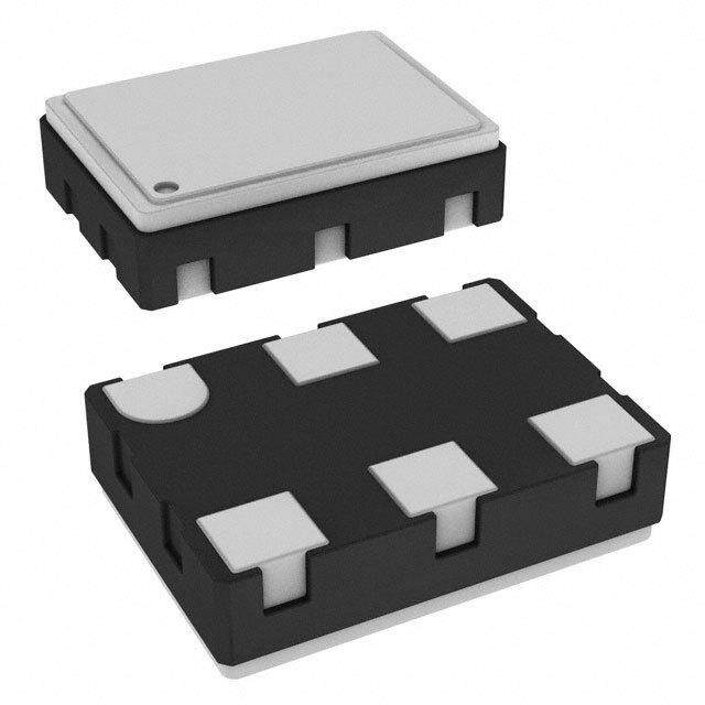
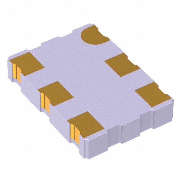
ICGOO电子元器件商城为您提供LTC6907HS6#TRMPBF由LINEAR TECHNOLOGY设计生产,在icgoo商城现货销售,并且可以通过原厂、代理商等渠道进行代购。 LTC6907HS6#TRMPBF价格参考。LINEAR TECHNOLOGYLTC6907HS6#TRMPBF封装/规格:时钟/计时 - 可编程计时器和振荡器, Oscillator, Silicon IC 40kHz ~ 4MHz TSOT-23-6。您可以下载LTC6907HS6#TRMPBF参考资料、Datasheet数据手册功能说明书,资料中有LTC6907HS6#TRMPBF 详细功能的应用电路图电压和使用方法及教程。
LTC6907HS6#TRMPBF 是 Linear Technology(现为 Analog Devices)生产的一款可编程计时器和振荡器,属于时钟/计时类器件。该型号的主要应用场景包括但不限于以下领域:

1. 电源管理:
   LTC6907 可用于生成精确的定时信号,适用于电源管理中的延迟控制、复位定时或看门狗定时功能。例如,在开关电源中,它可以用作软启动定时器或故障检测的延时电路。

2. 通信系统:
   在通信设备中,LTC6907 提供稳定的振荡信号,可用于数据传输的同步控制。例如,作为 UART 或 SPI 通信协议中的波特率发生器,确保数据收发的准确性。

3. 工业自动化:
   在工业控制系统中,LTC6907 能够实现周期性任务调度或事件触发功能。例如,用于传感器采样间隔的定时控制,或者驱动电机控制器中的脉冲宽度调制 (PWM) 信号。

4. 消费电子:
   在家用电器或便携式设备中,该芯片可用于生成低功耗的定时信号。例如,在智能手表或健康监测设备中,用作省电模式下的唤醒定时器。

5. 医疗设备:
   医疗仪器需要高精度的定时功能,LTC6907 可以提供稳定的时间基准。例如,在心率监测仪或血糖仪中,用作信号采样的定时源。

6. 汽车电子:
   在汽车应用中,LTC6907 可用于生成精确的定时信号,支持车载信息娱乐系统、发动机控制单元 (ECU) 或车身控制模块中的各种定时需求。

 特性与优势:
- 宽频率范围:支持从 0.1Hz 到 68MHz 的输出频率,适合多种应用场景。
- 低功耗设计:在电池供电设备中表现出色,有助于延长续航时间。
- 简单易用:通过外部电阻设置频率,无需复杂的外围电路。
- 高稳定性:采用 CMOS 工艺,确保温度变化和长时间运行时的稳定性。

总之,LTC6907HS6#TRMPBF 凭借其高性能和灵活性,广泛应用于需要精确定时和振荡信号的各种电子系统中。
| 参数 | 数值 |
| 产品目录 | 集成电路 (IC) |
| 描述 | IC OSC SILICON PROG TSOT23-6 |
| 产品分类 | |
| 品牌 | Linear Technology |
| 数据手册 | http://www.linear.com/docs/9059 |
| 产品图片 |
|
| 产品型号 | LTC6907HS6#TRMPBF |
| rohs | 无铅 / 符合限制有害物质指令(RoHS)规范要求 |
| 产品系列 | - |
| 供应商器件封装 | TSOT-23-6 |
| 其它名称 | LTC6907HS6#TRMPBF-ND |
| 包装 | 带卷 (TR) |
| 安装类型 | 表面贴装 |
| 封装/外壳 | SOT-23-6 细型,TSOT-23-6 |
| 工作温度 | -40°C ~ 125°C |
| 标准包装 | 500 |
| 电压-电源 | 3 V ~ 3.6 V |
| 电流-电源 | 305µA |
| 类型 | 振荡器 - 硅 |
| 计数 | - |
| 频率 | 40kHz ~ 4MHz |


- 商务部:美国ITC正式对集成电路等产品启动337调查
- 曝三星4nm工艺存在良率问题 高通将骁龙8 Gen1或转产台积电
- 太阳诱电将投资9.5亿元在常州建新厂生产MLCC 预计2023年完工
- 英特尔发布欧洲新工厂建设计划 深化IDM 2.0 战略
- 台积电先进制程称霸业界 有大客户加持明年业绩稳了
- 达到5530亿美元!SIA预计今年全球半导体销售额将创下新高
- 英特尔拟将自动驾驶子公司Mobileye上市 估值或超500亿美元
- 三星加码芯片和SET,合并消费电子和移动部门,撤换高东真等 CEO
- 三星电子宣布重大人事变动 还合并消费电子和移动部门
- 海关总署:前11个月进口集成电路产品价值2.52万亿元 增长14.8%


PDF Datasheet 数据手册内容提取
LTC6907 Micropower, 40kHz to 4MHz Resistor Set Oscillator in SOT-23 FEATURES DESCRIPTIOU ■ Supply Current: 36µA at 400kHz The LTC®6907 is a precision programmable oscillator that ■ 1% Frequency Accuracy (from 0°C to 70°C) is versatile, compact and easy to use. Micropower opera- ■ Frequency Range: 40kHz to 4MHz tion benefits portable and battery-powered equipment. At ■ One Resistor Sets the Oscillator Frequency 400kHz, the LTC6907 consumes 36µA on a 3V supply. ■ –40°C to 125°C Operating Temperature Range A single resistor programs the oscillator frequency over a ■ Start-Up Time Under 200µs at 4MHz 10:1 range with better than 0.65% initial accuracy. The ■ First Cycle After Power-Up is Accurate output frequency can be divided by 1, 3 or 10 to span a ■ 150Ω CMOS Output Driver 100:1 total frequency range, 40kHz to 4MHz. ■ Low Profile (1mm) SOT-23 (ThinSOTTM) Package The LTC6907 is easily programmed according to this APPLICATIOUS simple formula: ■ Low Cost Precision Programmable Oscillator ⎧10,DIVPiin= V+ 4MHz ⎛ 50k ⎞ ⎪ ■ Rugged, Compact Micropower Replacement for ƒOUT = •⎜ ⎟, N= ⎨3, DIVPin=Open Crystal and Ceramic Oscillators N ⎝RSET⎠ ⎪ 1, DIVPin=GND ⎩ ■ High Shock and Vibration Environments ■ Portable and Battery-Powered Equipment The LTC6907 is available in the 6-lead SOT-23 (ThinSOT) ■ PDAs and Cellular Phones package. , LT, LTC and LTM are registered trademarks of Linear Technology Corporation. ThinSOT is a trademark of Linear Technology Corporation. Contact LTC Marketing for a version of the part with a All other trademarks are the property of their respective owners. shutdown feature or lower frequency operation. TYPICAL APPLICATIOU Micropower Clock Generator Typical Supply Current vs Frequency LTC6907 40kHz TO 4MHz 1000 3V TO 3.6V V+ OUT CT L=O 2AD5° =C 5pF 0.1µF ÷10 GND GRD A)µ 3.3V, –:1 ÷3 DIV SET T ( 3.3V, –:3 ÷1 RSET EN 3.3V, –:10 50k TO 500k R UR 100 C 6907 TA01 Y L P P U S 10 10 100 1000 10000 OUTPUT FREQUENCY (kHz) 6907 TA02 6907fa 1
LTC6907 ABSOLUTE W AXIW UW RATIU GS PACKAGE/ORDER IU FORW ATIOU (Note 1) V+................................................................–0.3V to 6V TOP VIEW ORDER PART NUMBER DIV to GND....................................–0.3V to (V+ + 0.3V) OUT 1 6 V+ LTC6907CS6 SET to GND ...................................–0.3V to (V+ + 0.3V) GND 2 5 GRD LTC6907IS6 GRD to GND ..................................–0.3V to (V+ + 0.3V) DIV 3 4 SET LTC6907HS6 Operating Temperature Range (Note 7) S6 PACKAGE LTC6907C .......................................... –40°C to 85°C 6-LEAD PLASTIC TSOT-23 S6 PART MARKING* LTC6907I............................................ –40°C to 85°C TJMAX = 150°C, θJA = 200°C/W LTBTX LTC6907H ........................................ –40°C to 125°C Specified Temperature Range (Note 7) Order Options Tape and Reel: Add #TR Lead Free: Add #PBF Lead Free Tape and Reel: Add #TRPBF LTC6907C ...............................................0°C to 70°C Lead Free Part Marking: http://www.linear.com/leadfree/ LTC6907I............................................ –40°C to 85°C LTC6907H ........................................ –40°C to 125°C Consult LTC Marketing for parts specified with wider operating temperature ranges. *The temperature grade is indicated by a label on the shipping container. Storage Temperature Range................. –65°C to 150°C Lead Temperature (Soldering, 10 sec)..................300°C ELECTRICAL CHARACTERISTICS The ● denotes the specifications which apply over the full specified temperature range, otherwise specifications are at TA = 25°C. V+ = 3V to 3.6V, CL = 5pF, Pin 3 = V+ unless otherwise noted. All voltages are with respect to GND. SYMBOL PARAMETER CONDITIONS MIN TYP MAX UNITS ∆f Frequency Accuracy (Notes 2, 3) V+ = 3V to 3.6V 400kHz ≤ f ≤ 4MHz ±0.25 ±0.65 % 400kHz ≤ f ≤ 4MHz, LTC6907C ● ±1 % 400kHz ≤ f ≤ 4MHz, LTC6907I, H ● ±1.3 % RSET Frequency-Setting Resistor Range ● 50 500 kΩ ∆f/∆T Frequency Drift Over Temp (Note 3) RSET = 158k ● ±0.005 %/°C ∆f/∆V Frequency Drift Over Supply (Note 3) V+ = 3V to 3.6V, 50k ≤ RSET ≤ 500k 0.06 %/V Timing Jitter (Peak-to-Peak) (Note 4) Pin 3 = V+, 50k ≤ RSET ≤ 500k 0.12 % Pin 3 = Open, 50k ≤ RSET ≤ 500k 0.28 % Pin 3 = 0V, 50k ≤ RSET ≤ 500k 0.60 % Sf Long-Term Stability of Output Frequency Pin 3 = V+ 300 ppm/√kHr (Note 9) Stability Over 1 Year 888 ppm Stability Over 10 Years 2809 ppm DC Duty Cycle ● 43 50 57 % V+ Operating Supply Range (Note 8) ● 3 3.6 V IS Power Supply Current RSET = 500k, Pin 3 = 0V, RL = 10M V+ = 3.6V ● 40 55 µA (DIV = 1, fOUT = 400kHz) V+ = 3V ● 36 48 µA RSET = 50k, Pin 3 = 0V, RL = 10M V+ = 3.6V ● 305 406 µA (DIV = 1, fOUT = 4MHz) V+ = 3V ● 275 366 µA V High Level DIV Input Voltage V+ = 3.6V ● 3.1 V IH V+ = 3V ● 2.6 V V Low Level DIV Input Voltage V+ = 3.6V ● 0.5 V IL V+ = 3V ● 0.2 V IDIV DIV Input Current (Note 5) Pin 3 = V+ V+ = 3.6V ● 1 2 µA Pin 3 = 0V ● –2 –1 µA 6907fa 2
LTC6907 ELECTRICAL CHARACTERISTICS The ● denotes the specifications which apply over the full specified temperature range, otherwise specifications are at TA = 25°C. V+ = 3V to 3.6V, CL = 5pF, Pin 3 = V+ unless otherwise noted. All voltages are with respect to GND. SYMBOL PARAMETER CONDITIONS MIN TYP MAX UNITS VOH High Level Output Voltage (Note 5) V+ = 3.6V IOH = –100µA ● 3.40 3.57 V I = –1mA ● 3.10 3.45 V OH V+ = 3V IOH = –100µA ● 2.8 2.97 V I = –1mA ● 2.5 2.80 V OH VOL Low Level Output Voltage (Note 5) V+ = 3.6V IOL = 100µA ● 0.08 0.2 V I = 1mA ● 0.25 0.8 V OL V+ = 3V IOL = 100µA ● 0.07 0.2 V I = 1mA ● 0.25 0.8 V OL t OUT Rise Time (Note 6) V+ = 3.6V 10 ns r V+ = 3V 25 ns t OUT Fall Time (Note 6) V+ = 3.6V 10 ns f V+ = 3V 25 ns VGS GRD Pin Voltage Relative to SET Pin –10µA ≤ IGRD ≤ 0.3µA ● –10 10 mV Voltage Note 1: Stresses beyond those listed under Absolute Maximum Ratings Note 7: The LTC6907C is guaranteed to meet specified performance from may cause permanent damage to the device. Exposure to any Absolute 0°C to 70°C. The LTC6907C is designed, characterized and expected to Maximum Rating condition for extended periods may affect device meet specified performance from –40°C to 85°C but is not tested or QA reliability and lifetime. sampled at these temperatures. The LTC6907I is guaranteed to meet Note 2: Some frequencies may be generated using two different values of specified performance from –40°C to 85°C. R . For these frequencies, the error is specified assuming that the larger Note 8: Consult the Applications Information section for operation with SET value of R is used. supplies higher than 3.6V. SET Note 3: Frequency accuracy is defined as the deviation from the f Note 9: Long term drift on silicon oscillators is primarily due to the OUT equation. movement of ions and impurities within the silicon and is tested at 30°C Note 4: Jitter is the ratio of the peak-to-peak deviation of the period to the under otherwise nominal operating conditions. Long term drift is specified mean of the period. This specification is based on characterization and is as ppm/√kHr due to the typically non-linear nature of the drift. To calculate not 100% tested. drift for a set time period, translate that time into thousands of hours, take the square root and multiply by the typical drift number. For instance, a Note 5: Current into a pin is given as a positive value. Current out of a pin year is 8.77kHr and would yield a drift of 888ppm at 300ppm/√kHr. Ten is given as a negative value. years is 87.7kHr and would yield a drift of 2,809 ppm at 300 ppm/√kHr. Note 6: Output rise and fall times are measured between the 10% and Drift without power applied to the device may be approximated as 1/10th of 90% power supply levels. the drift with power, or 30ppm/√kHr for a 300ppm/√kHr device. 6907fa 3
LTC6907 TYPICAL PERFORW AU CE CHARACTERISTICS Typical Frequency Error Typical Frequency Error vs Power Supply Voltage vs Temperature Typical Frequency Error vs R SET 0.060% 1.0% 0.150% T = 25°C VV++ == 33VV T = 25°C CLOAD = 5pF 0.8% CCLLOOAADD == 55ppFF V+ = 3V 0.040% 0.6% 0.100% CLOAD = 5pF %) %) %) REQUENCY ERROR (–000...000202000%%% REQUENCY ERROR (––0000....24204%%%%% RSERT S=E T5 0=k 500k EQUENCY ERRROR (–000...000505000%%% F F R –0.6% F –0.040% –0.100% RSET = 50k –0.8% RSET = 500k –0.060% –1.0% –0.150% 3 3.1 3.2 3.3 3.4 3.5 3.6 –45 –25 –5 15 35 55 75 95 115 135 0 100 200 300 400 500 600 SUPPLY VOLTAGE (V) TEMPERATURE (°C) SET RESISTOR (k OHMS) 6907 G01 6907 G02 6907 G03 Typical Supply Current Typical Supply Current VSET vs Temperature (VSET is the vs Frequency vs Load Capacitance Voltage Measured at the SET Pin) 1000 CLOAD = 5pF 1000 T = 25°C 0.8 V+ = 3V T = 25°C 900 0.75 800 URRENT (A)µ 100 3.3V, –:10 3.3V, –:33.3V, –:1 URRENT (A)µ657000000 OLTAGE (V)0.006..576 C C V SUPPLY SUPPLY 432000000 RRRSSSEEETTT === 555000kk0,,k 33, ..306.VV0V R SET0.05.55 RSET = 500k, 3.6V 0.45 100 10 0 0.4 10 100 1000 10000 0 10 20 30 40 50 60 –45 –25 –5 15 35 55 75 95 115 135 OUTPUT FREQUENCY (kHz) LOAD CAPACITANCE (pF) TEMPERATURE (°C) 6907 G04 6907 G05 6907 G06 Output Waveform, 400kHz Output Waveform, 4MHz V+ = 3.3V V+ = 3.3V V V DI DI V/ V/ 0.5 0.5 6907 G07 6907 G08 500ns/DIV 50ns/DIV 6907fa 4
LTC6907 PIU FUU CTIOU S OUT (Pin 1): Oscillator Output. The OUT pin swings from or better temperature coefficient. For lower accuracy GND to V+ with an output resistance of approximately applications, an inexpensive 1% thick-film resistor may be 150Ω. For micropower operation, the load resistance used. Limit the capacitance in parallel with R to less SET must be kept as high as possible and the load capacitance than 10pF to reduce jitter and to ensure stability. The as low as possible. voltage on the SET pin is approximately 650mV at 25°C and decreases with temperature by about –2.3mV/°C. GND (Pin 2): Ground. GRD (Pin 5): Guard Signal. This pin can be used to reduce DIV (Pin 3): Divider Setting Input. This three-level input PC board leakage across the frequency setting resistor, selects one of three internal digital divider settings, deter- R . The GRD pin is held within a few millivolts of the SET mining the value of N in the frequency equation. Tie to GND SET pin and shunts leakage current away from the SET pin. To for ÷1, leave floating for ÷3 and tie to V+ for ÷10. When left control leakage, connect a bare copper trace (a trace with floating, the LTC6907 pulls Pin 3 to mid-supply with a no solder mask) to GRD and loop it around the SET pin and 2.5M resistor. When Pin 3 is floating, care should be taken all PC board metal connected to SET. Careful attention to to reduce coupling from the OUT pin and its trace to Pin 3. board layout and assembly can prevent leakage currents. Coupling can be reduced by increasing the physical space The use of a guard ring provides additional shielding of between traces or by shielding the DIV pin with grounded leakage currents from the SET pin and is optional. If metal. unused, the GRD pin should be left unconnected. SET (Pin 4): Frequency Setting Resistor Input. Connect a V+ (Pin 6): Voltage Supply (3V to 3.6V). A 0.1µF resistor, R , from this pin to GND to set the oscillator SET decoupling capacitor should be placed as close as pos- frequency. For best performance use a precision metal or sible to this pin for best performance. thin-film resistor of 0.1% or better tolerance and 50ppm/°C BLOCK DIAGRAW V+ FREQUENCY-TO-CURRENT V+ CONVERTERS 5M 6 fOSC THREE-LEVEL DIV INPUT 3 GND 2 IFB IFB DETECTOR 5M DIVIDER VSET ≅ VGRD ≅ 650mV SELECT ISET = IFB VSET 4 SET VSET – VOLTAGE fOSC 150Ω DRIVER PROGRAMMABLE CONTROLLED OUT RSET BUFFER OP AMP OSCILLATOR DIVIDER (n) 1 (÷1, ÷3, ÷10) GRD VSET + (MASTER OSCILLATOR) 5 50kΩ fOSC = 4MHz • RSET 6907 BD 6907fa 5
LTC6907 TEST CIRCUIT EQUIVALENT CIRCUIT OF OSCILLOSCOPE OR LTC6907 CTEST FREQUENCY COUNTER PROBE SUPPLY V+ OUT VOLTAGE 0.1µF GND GRD CPROBE R10PMROBE DIV SET RSET 0.01% 10ppm/°C 6907 F01 CTEST = 1/(1/5pF – 1/CPROBE) = 7.5pF FOR A 15pF SCOPE PROBE Figure 1. Test Circuit with 5pF Effective Load EQUIVALEU T IU PUT AU D OUTPUT CIRCUITS V+ V+ V+ 6 6 6 200Ω 20Ω TOTAL OUTPUT SET 1k GRD RESISTANCE 4 5 800pF GND GND GND 2 2 2 6907 F02 6907 F03 6907 F04 Figure 2. V+ Pin Figure 3. SET Pin Figure 4. GRD Pin V+ V+ 6 6 5M fOUT DIV OUT 150Ω 3 1 5M GND GND 2 2 6907 F05 6907 F06 Figure 5. DIV Pin Figure 6. OUT Pin 6907fa 6
LTC6907 THEORY OF OPERATIOU The LTC6907 is a precision, resistor programmable oscil- so lator (see Block Diagram). It generates a square wave at 1 the OUT pin with a period directly proportional to the value tOSC = =RSET •COSC (4) ƒ of an external resistor, R . A feedback circuit measures OSC SET and controls the oscillator frequency to achieve the high- The period and frequency are determined exclusively by est possible accuracy. In equilibrum, this circuit ensures R and the precision internal capacitor. Importantly, the SET that the current in the SET pin, I , is balanced by I . I SET FB FB value of V is immaterial, and the LTC6907 maintains its SET is proportional to the master oscillator frequency, so we accuracy even though V is not a precision reference SET have the relationship: voltage. I = I = V • ƒ • C (1) SET FB SET OSC OSC The digital dividers shown in the Block Diagram further Where C is a precision internal capacitor: divide the master oscillator frequency by 1, 3 or 10 OSC producing: C = 5pF for the LTC6907 OSC Solving for the oscillator period: ƒ OSC ƒ = (5) OUT N 1 V tOSC = = SET •COSC (2) and ƒ I OSC SET t = N • t (6) OUT OSC This is the fundamental equation for the LTC6907. It holds Table 1 gives specific frequency and period equations for regardless of how the SET pin is driven. When a resistor, the LTC6907. The Applications Information section gives R , is connected from the SET pin to ground, we have SET further detail and discusses alternative ways of setting the the relationship: LTC6907 output frequency. V SET =RSET (3) I SET Table 1. Output Frequency Equations PART NUMBER FREQUENCY PERIOD DIVIDER RATIOS LTC6907 ⎧10,DIVPin= V+ ƒOUT = 4MNHz •⎛⎝⎜R50k ⎞⎠⎟ tOUT =N•250ns•⎛⎝⎜R5S0EkT⎞⎠⎟ N=⎨⎪3, DIVPin=Open SET ⎪ 1, DIVPin=GND ⎩ 6907fa 7
LTC6907 APPLICATIOU S IU FORW ATIOU Selecting R and the Divider Ratio 10000 SET ÷1 ÷3 The LTC6907 contains a master oscillator followed by a ÷10 digital divider (see Block Diagram). R determines the Hz) SET k master oscillator frequency and the three level DIV pin sets CY ( 1000 N E the divider ratio, N. The range of frequencies accessible in U Q E each divider ratio overlap, as shown in Figure7. This FR T figure is derived from the equations in Table 1. For any PU 100 T U given frequency, power can be minimized by minimiz- O ing the master oscillator frequency. This implies maxi- mizing R and using the lowest possible divider ratio, 10 SET 10 100 1000 N. The relationship between RSET, N and the unloaded RSET (kΩ) power consumption is shown in Figure 8. The supply 6907 F07 current decreases for large values of RSET. Refer to the Figure 7. RSET vs Desired Output Frequency section titled “Jitter and Divide Ratio.” 160 CLOAD = 0 Minimizing Power Consumption 140 ISUPPLY V+ = 3V DIV = –:1 The supply current of the LTC6907 has four current A) 120 TA = 25°C µ components: T ( 100 N E R • Constant (Independent V+, ƒOUT and CLOAD) CUR 80 LY 60 • Proportional to I (which is the current in R ) P SET SET P U S 40 • Proportional to V+, ƒ and C OUT LOAD 20 • Proportional to V+ and R LOAD 0 10 100 1000 An approximate expression for the total supply current is: RSET (kΩ) 6907 F08 V+ Figure 8. Unloaded Supply Current vs RSET I+≅7µA+6•I +V+ •ƒ •(C +5pF)+ SET OUT LOAD 2•R LOAD Guarding Against PC Board Leakage oor,intermsofV , SET The LTC6907 uses relatively large resistance values for V V+ I+ ≅7µA+6• SET +V+ •ƒ ••(C +5pF)+ RSET to minimize power consumption. For RSET = 500k, OUT LOAD RSET 2•RLOAD the SET pin current is typically only 13µA. Thus, only 13nA leaking into the SET pin causes a 0.1% frequency error. VSET is approximately 650mV at 25°C, but varies with Similarly, 500M of leakage resistance across RSET temperature. This behavior is shown in the Typical Perfor- (1000 • R ) causes the same 0.1% error. SET mance Characteristics. Achieving the highest accuracy requires controlling po- Power can be minimized by maximizing RSET, minimizing tential leakage paths. PC board leakage is aggravated by the load on the OUT pin and operating at lower frequen- both dirt and moisture. Effective cleaning is a good first cies. Figure 9 shows total supply current vs frequency step to minimizing leakage. under typical conditions. Below 100kHz the load current is Another effective method for controlling leakage is to shunt negligible for the 5pF load shown. the leakage current away from the sensitive node through a low impedance path. The LTC6907 provides a signal on the GRD pin for this purpose. Figure 10 shows a PC board 6907fa 8
LTC6907 APPLICATIOU S IU FORW ATIOU 1000 Power Supply Rejection CLOAD = 5pF T = 25°C The LTC6907 has a very low supply voltage coefficient, A) 3.3V, –:1 meaning that the output frequency is nearly insensitive to µ T ( 3.3V, –:3 the DC power supply voltage. In most cases, this error N URRE 100 3.3V, –:10 term can be neglected. C LY High frequency noise on the power supply (V+) pin has the P P SU potential to interfere with the LTC6907’s master oscillator. Periodic noise, such as that generated by a switching power supply, can shift the output frequency or increase 10 10 100 1000 10000 jitter. The risk increases when the fundamental frequency OUTPUT FREQUENCY (kHz) or harmonics of the noise fall near the master oscillator 6907 F09 Figure 9. Supply Current vs Frequency over DIV Settings frequency. It is relatively easy to filter the LTC6907 power supply because of the very low supply current. For ex- layout that uses the GRD pin and a “guard ring” to absorb ample, an RC filter with R = 160Ω and C = 10µF provides leakage currents. The guard ring surrounds the SET pin a 100Hz lowpass filter while dropping the supply voltage and the end of R to which it is connected. The guard ring SET only about 10mV. must have no solder mask covering it to be effective. The GRD pin voltage is held within a few millivolts of the SET Operating the LTC6907 with Supplies Higher pin voltage, so any leakage path between the SET pin and Than 3.6V the guard ring generates no leakage current. The LTC6907 may also be used with supply voltages Start-Up Time between 3.6V and 5.5V under very specific conditions. To ensure proper functioning above 3.6V, a filter circuit must When the LTC6907 is powered up, it holds the OUT pin be attached to the power supply and located within 1cm of low. After the master oscillator has settled, the OUT pin is the device. A simple RC filter consisting of a 100Ω resistor enabled and the first output cycle is accurate. The time and 1µF capacitor (Figure 11) will ensure that supply from power-up to the first output transition is given resonance at higher supply voltages does not induce approximately by: unpredictable oscillator behavior. Accuracy under higher t ≅ 64 • t + 100µs supplies may be estimated from the typical Frequency vs START OSC Supply Voltage curves in the Typical Performance Charac- The digital divider ratio, N, does not affect the start- teristics section of this data sheet. up time. V+ LTC6907 3.6V TO 5.5V DC 1 OUT V+ 6 NO SOLDER MASK OVER THE GUARD RING 100Ω LTC6907 GRD V+ OUT 2 GND 5 1µF GND GRD GUARD RING DIV SET 3 DIV SET 4 RSET RSET NO LEAKAGE 6907 F11 CURRENT Figure 11. Using the LTC6907 at Higher Supply Voltages LEAKAGE CURRENT 6907 F10 Figure 10. PC Board Layout with Guard Ring 6907fa 9
LTC6907 APPLICATIOU S IU FORW ATIOU Alternative Methods for Setting the Output Frequency Figure 12 and Figure 13 show a current controlled oscilla- tor and a voltage controlled oscillator. These circuits are Any means of sinking current from the SET pin will control not highly accurate if used alone, but can be very useful if the output frequency of the LTC6907. Equation2 (re- they are enclosed in an overall feedback circuit such as a peated below) gives the fundamental relationship between phase-locked loop. frequency and the SET pin voltage and current: 1 V tOSC = = SET •5pF (2) ƒ I OSC SET LTC6907 4MHz TO 400kHz V+ V+ OUT 0µA This equation shows that the LTC6907 converts conduc- GND GRD TO 11.25µA 10k tance (I /V ) to frequency or, equivalently, converts SET SET DIV SET resistance (R = V /I ) to period. SET SET SET 49.9k V is the voltage across an internal diode, and as such SET 6907 F12 it is given approximately by: Figure 12. Current Controlled Oscillator I V ≅ V •Log SET SET T e IS LTC6907 4MHz TO 400kHz V+ V+ OUT ⎛ I ⎞ ≅25.9mV•Log SET –2.3mV/°C GND GRD e⎜ ⎟ ⎝82•10–18A⎠ DIV SET VCTRL RSET 0V TO 0.675V (VSET) 499k 56.2k where 6907 F13 V = kT/q = 25.9mV at T = 300°K (27°C) T Figure 13. Voltage Controlled Oscillator I ≅ 82 • 10–18 Amps S (I is also temperature dependent) S Jitter and Divide Ratio V varies with temperature and the SET pin current. The SET At a given output frequency, a higher master oscillator response of V to temperature is shown in the Typical SET frequency and a higher divide ratio will result in lower jitter Performance graphs. V changes approximately –2.3mV/ SET and higher power supply dissipation. Indeterminate jitter °C. At room temperature V increases 18mV/octave or SET percentage will decrease by a factor of slightly less than 60mV/decade of increase in I . SET the square root of the divider ratio, while determinate jitter If the SET pin is driven with a current source generating will not be similarly attenuated. Please consult the speci- I , the oscillator output frequency will be: fication tables for typical jitter at various divider ratios. SET I SET 5pF ƒ ≅ OSC ⎛ I ⎞ 25.9mV•Log SET –22.3mV/°C e⎝⎜82•10–18A⎠⎟ 6907fa 10
LTC6907 PACKAGE DESCRIPTIOU S6 Package 6-Lead Plastic TSOT-23 (Reference LTC DWG # 05-08-1636) 2.90 BSC 0.62 0.95 (NOTE 4) MAX REF 1.22 REF 1.50 – 1.75 3.85 MAX 2.62 REF 1.4 MIN 2.80 BSC (NOTE 4) PIN ONE ID RECOMMENDED SOLDER PAD LAYOUT 0.30 – 0.45 0.95 BSC PER IPC CALCULATOR 6 PLCS (NOTE 3) 0.80 – 0.90 0.20 BSC 0.01 – 0.10 1.00 MAX DATUM ‘A’ 0.30 – 0.50 REF 1.90 BSC 0.09 – 0.20 (NOTE 3) S6 TSOT-23 0302 NOTE: 1. DIMENSIONS ARE IN MILLIMETERS 4. DIMENSIONS ARE EXCLUSIVE OF MOLD FLASH AND METAL BURR 2. DRAWING NOT TO SCALE 5. MOLD FLASH SHALL NOT EXCEED 0.254mm 3. DIMENSIONS ARE INCLUSIVE OF PLATING 6. JEDEC PACKAGE REFERENCE IS MO-193 6907fa Information furnished by Linear Technology Corporation is believed to be accurate and reliable. 11 However, no responsibility is assumed for its use. Linear Technology Corporation makes no represen- tation that the interconnection of its circuits as described herein will not infringe on existing patent rights.
LTC6907 TYPICAL APPLICATIOUS Sine Wave Oscillator Setting Frequency to 0.1% Trimming the Frequency Resolution with Standard Resistors 2MHz WITH 1MHz LTC6907 ±2.5% RANGE 3V TO 3.6V V+LTC69O07UT 0.1µF 1k 3V TO 3.6V V+LTC69O07UT 40kHz TO 4MHz 3V TO 3.60V.1µF VG+ND GORUDT 0.1µF 0.1µF GND GRD GND GRD L1 C1 ÷10 DIV SET DIV SET RSET 100µH 220pF ÷÷13 DIV SET RR1%AA <T HRIBN/1 F0ILM R97A.6k 200k 6907 TA05 RB RB 50k TO 500k 5k 0.1% THIN FILM 6907 TA03 6907 TA04 Low Power 62.5Hz to 6.25kHz Sine Wave Generator (I < 1.5mA) Q fOSC = 400kHz TO 40kHz 3V 1 V+ OUT 5 LTC6907 1µF 2 GND GRD 3 4 56.2k DIV SET 499k V0VCT–R0L.6V fOSC LTC1067-50 3V C4 C3 1 V+ CLK 16 74HC4520 1µF 0.1µF 2 15 NC AGND 1 CLOCK A Q1A 3 ÷2 R61 3 V+ V– 14 R62 14k 3V 2 ENABLE A Q2A 4 ÷4 10k 4 SA SB 13 R52 C2 1160 VENDDABLE B QQ34AA 56 ÷÷186 RR3511 5 51..111kk 56 LBPPAA BLPPBB 1121 R32 51.15k.11k SOIUNTEWAVE 0.1µF 7 RESET A Q1B 11 ÷32 R11 7 HPA/NA HPB/NB 10 8 VSS Q2B 12 ÷64 100k R21 20k 8 INV A INV B 9 R22 20k fSINE = fOSC 9 13 ÷128 64 CLOCK B Q3B 15 14 ÷256 RH1 249k RESET B Q4B fOSC 64 RL1 51.1k 6907 TA06 CLOCK-TUNABLE LOWPASS FILTER WITH A STOPBAND NOTCH AT THE 3rd HARMONIC (fOSC• 3) 64 RELATED PARTS PART NUMBER DESCRIPTION COMMENTS LTC1799 1kHz to 33MHz ThinSOT Oscillator, Resistor Set Wide Frequency Range LTC6900 1kHz to 20MHz ThinSOT Oscillator, Resistor Set Low Power, Wide Frequency Range LTC6902 Multiphase Oscillator with Spread Spectrum Modulation 2-, 3- or 4-Phase Outputs LTC6903/LTC6904 1kHz to 68MHz Serial Port Programmable Oscillator 0.1% Frequency Resolution, I2C or SPI Interface LTC6905 17MHz to 170MHz ThinSOT Oscillator, Resistor Set High Frequency, 100µsec Startup, 7ps RMS Jitter LTC6905-XXX Fixed Frequency ThinSOT Oscillator Family, up to 133MHz No Trim Components Required LTC6906 Micropower 10kHz to 1MHz ThinSOT Oscillator, Resistor Set 12µA Supply Current of 100kHz, 0.65% Frequency Accuracy 6907fa 12 Linear Technology Corporation LT 0506 REV A • PRINTED IN USA 1630 McCarthy Blvd., Milpitas, CA 95035-7417 (408) 432-1900 ● FAX: (408) 434-0507 ● www.linear.com © LINEAR TECHNOLOGY CORPORATION 2005
Mouser Electronics Authorized Distributor Click to View Pricing, Inventory, Delivery & Lifecycle Information: A nalog Devices Inc.: LTC6907CS6#TRPBF LTC6907HS6#TRPBF LTC6907IS6#TRM LTC6907HS6 LTC6907IS6#TR LTC6907IS6#TRPBF LTC6907CS6 LTC6907CS6#TRM LTC6907IS6#PBF LTC6907HS6#TRM LTC6907CS6#TR LTC6907HS6#TR LTC6907HS6#TRMPBF LTC6907IS6 LTC6907CS6#TRMPBF LTC6907IS6#TRMPBF LTC6907CS6#PBF LTC6907HS6#PBF