ICGOO在线商城 > 集成电路(IC) > 时钟/计时 - 可编程计时器和振荡器 > TLC556CD
 Datasheet下载
- 型号: TLC556CD
- 制造商: Texas Instruments
- 库位|库存: xxxx|xxxx
- 要求:
| 数量阶梯 | 香港交货 | 国内含税 |
| +xxxx | $xxxx | ¥xxxx |
查看当月历史价格
查看今年历史价格
TLC556CD产品简介:
ICGOO电子元器件商城为您提供TLC556CD由Texas Instruments设计生产,在icgoo商城现货销售,并且可以通过原厂、代理商等渠道进行代购。 TLC556CD价格参考。Texas InstrumentsTLC556CD封装/规格:时钟/计时 - 可编程计时器和振荡器, 555 Type, Timer/Oscillator (Dual) IC 2.1MHz 14-SOIC。您可以下载TLC556CD参考资料、Datasheet数据手册功能说明书,资料中有TLC556CD 详细功能的应用电路图电压和使用方法及教程。
TLC556CD 是 Texas Instruments(德州仪器)生产的一款双路可编程定时器/振荡器芯片,属于时钟/计时类器件。它基于经典的555定时器架构,但集成两个独立的定时器电路,并具备较低功耗和更宽的工作电压范围(通常为2V至15V),适用于多种模拟和数字定时应用。

 应用场景包括:

1. 脉冲发生器:用于生成精确的时间延迟或脉冲信号,常见于工业控制、测量设备和自动测试系统中。

2. 振荡器电路:可用于构建方波、锯齿波等波形发生器,广泛应用于音频设备、信号发生器和频率合成器中。

3. 定时控制:如定时开关、定时报警器、定时照明系统等,适用于家电、安防系统和自动化设备。

4. PWM信号生成:用于调节电机转速、LED亮度控制、电源管理等场合。

5. 传感器接口电路:将传感器的模拟信号转换为时间或频率信号,便于后续处理。

6. 教育与实验:因其结构简单、功能灵活,常用于电子教学实验中,帮助学生理解定时器和振荡器的工作原理。

TLC556CD 适合对成本敏感、空间受限但需要可靠定时功能的中低精度应用。
| 参数 | 数值 |
| 产品目录 | 集成电路 (IC)半导体 |
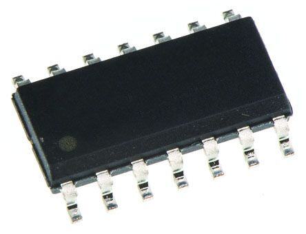
| 描述 | IC OSC TIMER DUAL 2.1MHZ 14-SOIC计时器和支持产品 Dual CMOS |
| 产品分类 | |
| 品牌 | Texas Instruments |
| 产品手册 | |
| 产品图片 |
|
| rohs | 符合RoHS无铅 / 符合限制有害物质指令(RoHS)规范要求 |
| 产品系列 | 时钟和计时器IC,计时器和支持产品,Texas Instruments TLC556CDLinCMOS™ |
| 数据手册 | |
| 产品型号 | TLC556CD |
| 产品目录页面 | |
| 产品种类 | 计时器和支持产品 |
| 供应商器件封装 | 14-SOIC |
| 其它名称 | 296-10342-5 |
| 内部定时器数量 | 2 |
| 包装 | 管件 |
| 单位重量 | 122.400 mg |
| 商标 | Texas Instruments |
| 安装类型 | 表面贴装 |
| 安装风格 | SMD/SMT |
| 封装 | Tube |
| 封装/外壳 | 14-SOIC(0.154",3.90mm 宽) |
| 封装/箱体 | SOIC-14 |
| 工作温度 | 0°C ~ 70°C |
| 工厂包装数量 | 50 |
| 最大功率耗散 | 950 mW |
| 最大工作温度 | + 70 C |
| 最小工作温度 | 0 C |
| 标准包装 | 50 |
| 电压-电源 | 2 V ~ 18 V |
| 电流-电源 | 720µA |
| 电源电压-最大 | 15 V |
| 电源电压-最小 | 2 V |
| 电源电流 | 130 uA |
| 类型 | 555 型,计时器/振荡器(双路) |
| 系列 | TLC556 |
| 计数 | - |
| 频率 | 2.1MHz |


- 商务部:美国ITC正式对集成电路等产品启动337调查
- 曝三星4nm工艺存在良率问题 高通将骁龙8 Gen1或转产台积电
- 太阳诱电将投资9.5亿元在常州建新厂生产MLCC 预计2023年完工
- 英特尔发布欧洲新工厂建设计划 深化IDM 2.0 战略
- 台积电先进制程称霸业界 有大客户加持明年业绩稳了
- 达到5530亿美元!SIA预计今年全球半导体销售额将创下新高
- 英特尔拟将自动驾驶子公司Mobileye上市 估值或超500亿美元
- 三星加码芯片和SET,合并消费电子和移动部门,撤换高东真等 CEO
- 三星电子宣布重大人事变动 还合并消费电子和移动部门
- 海关总署:前11个月进口集成电路产品价值2.52万亿元 增长14.8%


PDF Datasheet 数据手册内容提取
TLC556, TLC556Y DUAL LinCMOS TIMERS SLFS047B – FEBRUARY 1984 – REVISED SEPTEMBER 1997 (cid:0) Very Low Power Consumption...2 mW D, J, OR N PACKAGE Typ at VDD = 5 V (TOP VIEW) (cid:0) Capable of Operation in Astable Mode (cid:0) CMOS Output Capable of Swinging Rail to 1 DISCH 1 14 VDD Rail 1 THRES 2 13 2 DISCH (cid:0) 1 CONT 3 12 2 THRES High Output-Current Capability 1 RESET 4 11 2 CONT Sink 100 mA Typ 1 OUT 5 10 2 RESET Source 10 mA Typ (cid:0) 1 TRIG 6 9 2 OUT Output Fully Compatible With CMOS, TTL, GND 7 8 2 TRIG and MOS (cid:0) Low Supply Current Reduces Spikes FK PACKAGE During Output Transitions (TOP VIEW) (cid:0) Single-Supply Operation From 2 V to 15 V (cid:0) S H H Functionally interchangeable With the E C C R NE556; Has Same Pinout TH DIS C DDDIS 1 1 NV 2 description 3 2 1 20 19 1 CONT 4 18 2 THRES The TLC556 series are monolithic timing circuits fabricated using the TI LinCMOS process, which NC 5 17 NC 1 RESET 6 16 2 CONT provides full compatibility with CMOS, TTL, and NC 7 15 NC MOS logic and operates at frequencies up to 1 OUT 8 14 2 RESET 2MHz. Accurate time delays and oscillations are 9 10 11 12 13 possible with smaller, less-expensive timing capacitors than the NE556 because of the high G D CG T iancpruots si mthpee fdualln rcaen.g eP oofw peorw ceor nssuupmplpyt ivoonlt aigse slo.w 1 TRI GN N2 TRI 2 OU Like the NE556, the TLC556 has a trigger level NC–No internal connection approximately one-third of the supply voltage and a threshold level approximately two-thirds of the supply voltage. These levels can be altered by use of the control voltage terminal. When the trigger input falls below the trigger level, the flip-flop is set and the output goes high. If the trigger input is above the trigger level and the threshold input is above the threshold level, the flip-flop is reset and the output is low. The reset input can override all other inputs and can be used to initiate a new timing cycle. If the reset input is low, the flip-flop is reset and the output is low. Whenever the output is low, a low-impedance path is provided between the discharge terminal and ground. While the CMOS output is capable of sinking over 100 mA and sourcing over 10 mA, the TLC556 exhibits greatly reduced supply-current spikes during output transitions. This minimizes the need for the large decoupling capacitors required by the NE556. These devices have internal electrostatic-discharge (ESD) protection circuits that prevent catastrophic failures at voltages up to 2000 V as tested under MIL-STD-883C, Method 3015. However, care should be exercised in handling these devices, as exposure to ESD may result in degradation of the device parametric performance. All unused inputs should be tied to an appropriate logic level to prevent false triggering. The TLC556C is characterized for operation from 0°C to 70°C. The TLC556I is characterized for operation from –40°C to 85°C. The TLC556M is characterized for operation over the full military temperature range of –55°C to 125°C. LinCMOS is a trademark of Texas Instruments Incorporated. PRODUCTION DATA information is current as of publication date. Copyright 1997, Texas Instruments Incorporated Products conform to specifications per the terms of Texas Instruments standard warranty. Production processing does not necessarily include testing of all parameters. POST OFFICE BOX 655303 • DALLAS, TEXAS 75265 1
TLC556, TLC556Y DUAL LinCMOS TIMERS SLFS047B – FEBRUARY 1984 – REVISED SEPTEMBER 1997 AVAILABLE OPTIONS PACKAGE TTAA VVDDDD CCHHIIPP FFOORRMM SMALL OUTLINE CHIP CARRIER CERAMIC DIP PLASTIC DIP RANGE RANGE (Y) (D) (FK) (J) (N) O°C 2 V to to TLC556CD TLC556CN TLC556Y 70°C 18 V –4O°C 3 V to to TLC556lD TLC556IN 85°C 18 V –55°C 5 V to to TLC556MD TLC556MFK TLC556MJ TLC556MN 125°C 18 V The D package is available taped and reeled. Add the suffix R to the device type (e.g., TLC556CDR). FUNCTION TABLE RESET TRIGGER THRESHOLD DISCHARGE OUTPUT VOLTAGE† VOLTAGE† VOLTAGE† SWITCH < MIN Irrelevant Irrelevant L On > MAX < MIN Irrelevant H Off >MAX >MAX >MAX L On > MAX > MAX < MIN As previously established †For conditions shown as MIN or MAX, use the appropriate value specified under electrical characteristics. functional block diagram (each timer) CONT VDD 3 RESET 14 4 R 2 R1 THRES 5 R 1 OUT S R 6 TRIG R 1 DISCH 7 GND RESET can override TRIG and THRES. TRIG can override THRES. Pin numbers shown are for the D, J, or N packages. 2 POST OFFICE BOX 655303 • DALLAS, TEXAS 75265
TLC556, TLC556Y DUAL LinCMOS TIMERS SLFS047B – FEBRUARY 1984 – REVISED SEPTEMBER 1997 TLC556Y chip information These chips, properly assembled, display characteristics similar to the TLC556 (see electrical table). Thermal compression or ultrasonic bonding may be used on the doped aluminum bonding pads. Chips may be mounted with conductive epoxy or a gold-silicon preform. BONDING PAD ASSIGNMENTS CHIP THICKNESS: 15 TYPICAL BONDING PADS: 4 × 4 MINIMUM TJ max = 150°C 61 TOLERANCES ARE ±10% ALL DIMENSIONS ARE IN MILS NO BACKSIDE METALLIZATION PIN (7) INTERNALLY CONNECTED TO BACKSIDE OF CHIP 97 FUNCTIONAL BLOCK DIAGRAM (EACH TIMER) CONT VDD (3) RESET (14) (4) R (2) R1 THRESH (5) R 1 OUT S R (6) TRIG R (1) DISCH (7) GND POST OFFICE BOX 655303 • DALLAS, TEXAS 75265 3
TLC556, TLC556Y DUAL LinCMOS TIMERS SLFS047B – FEBRUARY 1984 – REVISED SEPTEMBER 1997 absolute maximum ratings over operating free-air temperature (unless otherwise noted) TLC556C TLC556I TLC556M UNIT Supply voltage, VDD (see Note 1) 18 18 18 V Input voltage range, VI –0.3 to VDD –0.3 to VDD –0.3 to VDD V Sink current, discharge or output 150 150 150 mA Source current, output 15 15 15 mA Continuous total power dissipation See Dissipation Rating Table Operating free-air temperature range 0 to 70 –40 to 85 –55 to 125 °C Storage temperature range –65 to 150 –65 to 150 –65 to 150 °C Case temperature for 60 seconds FK package 260 Lead temperature 1,6 mm (1/16 inch) from case for 60 seconds J package 300 °C Lead temperature 1,6 mm (1/16 inch) from case for 10 seconds D or N package 260 260 NOTE 1: All voltage values are with respect to network ground terminal. DISSIPATION RATING TABLE TA ≤ 25°C DERATING FACTOR TA = 70°C TA = 85°C TA = 125°C PACKAGE POWER RATING ABOVE TA = 25°C POWER RATING POWER RATING POWER RATING D 950 mW 7.6 mW/°C 608 mW 494 mW N/A FK 1375 mW 11.0 mW/°C 880 mW 715 mW 275 mW J 1375 mW 11.0 mW/°C 880 mW 715 mW 275 mW N 1150 mW 9.2 mW/°C 736 mW 598 mW N/A recommended operating conditions MIN MAX UNIT Supply voltage, VDD 2 15 V TLC556C 0 70 Operating free-air temperature range, TA TLC556I –40 85 °C TLC556M –55 125 4 POST OFFICE BOX 655303 • DALLAS, TEXAS 75265
TLC556, TLC556Y DUAL LinCMOS TIMERS SLFS047B – FEBRUARY 1984 – REVISED SEPTEMBER 1997 electrical characteristics at specified free-air temperature, V = 2 V for TLC556C, V = 3 V for DD DD TLC556I TEST TLC556C TLC556I PPAARRAAMMEETTEERR CONDITIONS TTAA†† MIN TYP MAX MIN TYP MAX UUNNIITT 25°C 0.95 1.33 1.65 1.6 2 2.4 VVIITT IInnppuutt tthhrreesshhoolldd vvoollttaaggee VV Full range 0.85 1.75 1.5 2.5 25°C 10 10 TThhrreesshhoolldd ccuurrrreenntt ppAA MAX 75 150 25°C 0.4 0.67 0.95 0.71 1 1.29 VV((ttriigger)) TTrriiggggeerr vvoollttaaggee VV Full range 0.3 1.05 0.61 1.39 25°C 10 10 II((ttriigger)) TTrriiggggeerr ccuurrrreenntt ppAA MAX 75 150 25°C 0.4 1.1 1.5 0.4 1.1 1.5 VV((resett)) RReesseett vvoollttaaggee VV Full range 0.3 1.8 0.3 1.8 25°C 10 10 II((resett)) RReesseett ccuurrrreenntt ppAA MAX 75 150 Control voltage (open circuit) as MAX 66.7% 66.7% a percentage of supply voltage Dischargge switch on-state volt- 25°C 0.04 0.2 0.03 0.2 IIOOLL == 11 mmAA VV age Full range 0.25 0.375 Dischargge switch off-state cur- 25°C 0.1 0.1 nnAA rent MAX 0.5 120 25°C 1.5 1.9 1.5 1.9 VVOOHH HHiigghh-lleevveell oouuttppuutt vvoollttaaggee IIOOHH == –330000 mm AA VV Full range 1.5 2.5 25°C 0.07 0.3 0.07 0.3 VVOOLL LLooww-lleevveell oouuttppuutt vvoollttaaggee IIOOLL == 11 mmAA VV Full range 0.35 0.4 25°C 130 500 130 500 IIDDDD SSuuppppllyy ccuurrrreenntt SSeeee NNoottee 22 mm AA Full range 800 1000 †Full range is 0°C to 70°C for TLC556C and –40°C to 85°C for TLC556I. NOTE 2: These values apply for the expected operating configurations in which THRES is connected directly to DISCH or TRIG. POST OFFICE BOX 655303 • DALLAS, TEXAS 75265 5
TLC556, TLC556Y DUAL LinCMOS TIMERS SLFS047B – FEBRUARY 1984 – REVISED SEPTEMBER 1997 electrical characteristics at specified free-air temperature, V = 5 V DD TEST TLC556C TLC556I TLC556M PPAARRAAMMEETTEERR CONDITIONS TTAA†† MIN TYP MAX MIN TYP MAX MIN TYP MAX UUNNIITT Input threshold 25°C 2.8 3.3 3.8 2.8 3.3 3.8 2.8 3.3 3.8 VVIT voltage Full range 2.7 3.9 2.7 3.9 2.7 3.9 VV 25°C 10 10 10 TThhrreesshhoolldd ccuurrrreenntt ppAA MAX 75 150 5000 25°C 1.36 1.66 1.96 1.36 1.66 1.96 1.36 1.66 1.96 VV((trigger)) TTrriiggggeerr vvoollttaaggee VV Full range 1.26 2.06 1.26 2.06 1.26 2.06 25°C 10 10 10 II((triigger)) TTrriiggggeerr ccuurrrreenntt ppAA MAX 75 150 5000 25°C 0.4 1.1 1.5 0.4 1.1 1.5 0.4 1.1 1.5 VV((reset)) RReesseett vvoollttaaggee VV Full range 0.3 1.8 0.3 1.8 0.3 1.8 25°C 10 10 10 II((reset)) RReesseett ccuurrrreenntt ppAA MAX 75 150 5000 Control voltage (open circuit) as a MAX 66.7% 66.7% 66.7% percentage of supply voltage Dischargge switch 25°C 0.15 0.5 0.15 0.5 0.15 0.5 on-state voltage IIOOL = 1100 mmAA Full range 0.6 0.6 0.6 VV Dischargge switch 25°C 0.1 0.1 0.1 nnAA off-state current MAX 0.5 2 120 Higgh-level output 25°C 4.1 4.8 4.1 4.8 4.1 4.8 VVOOH voltage IIOOH = –11 mmAA Full range 4.1 4.1 4.1 VV 25°C 0.21 0.4 0.21 0.4 0.21 0.4 IIOOL = 88 mmAA Full range 0.5 0.5 0.6 Low-level output 25°C 0.13 0.3 0.13 0.3 0.13 0.3 VVOOL voltage IIOOL = 55 mmAA Full range 0.4 0.4 0.45 VV 25°C 0.08 0.3 0.08 0.3 0.08 0.3 IIOOL = 33.22 mmAA Full range 0.35 0.35 0.4 25°C 340 700 340 700 340 700 IIDDDD SSuuppppllyy ccuurrrreenntt SSeeee NNoottee 22 mm AA Full range 1000 1200 1400 †Full range is 0°C to 70°C for TLC556C, –40°C to 85°C for TLC556I, and –55°C to 125°C for TLC556M. NOTE 2: These values apply for the expected operating configurations in which THRES is connected directly to DISCH or to TRIG. 6 POST OFFICE BOX 655303 • DALLAS, TEXAS 75265
TLC556, TLC556Y DUAL LinCMOS TIMERS SLFS047B – FEBRUARY 1984 – REVISED SEPTEMBER 1997 electrical characteristics at specified free-air temperature, V = 15 V DD PPAARRAAMMEETTEERR CONTDEISTTIONS TTAA†† MINTLCT5Y5P6C MAX MIN TLCT5Y5P6I MAX MINTLCT5Y5P6M MAX UUNNIITT 25°C 9.45 10 10.55 9.45 10 10.55 9.45 10 10.55 VVIITT IInnppuutt tthhrreesshhoolldd vvoollttaaggee VV Full range 9.35 10.65 9.35 10.65 9.35 10.65 25°C 10 10 10 TThhrreesshhoolldd ccuurrrreenntt ppAA MAX 75 150 5000 25°C 4.65 5 5.35 4.65 5 5.35 4.65 5 5.35 VV((ttriigger)) TTrriiggggeerr vvoollttaaggee VV Full range 4.55 5.45 4.55 5.45 4.55 5.45 25°C 10 10 10 II((ttriigger)) TTrriiggggeerr ccuurrrreenntt ppAA MAX 75 150 5000 25°C 0.4 1.1 1.5 0.4 1.1 1.5 0.4 1.1 1.5 VV((resett)) RReesseett vvoollttaaggee VV Full range 0.3 1.8 0.3 1.8 0.3 1.8 25°C 10 10 10 II((resett)) RReesseett ccuurrrreenntt ppAA MAX 75 150 5000 Control voltage (open circuit) as a percent- MAX 66.7% 66.7% 66.7% age of supply voltage Dischargge switch on- 25°C 0.8 1.7 0.8 1.7 0.8 1.7 state voltage IIOOLL == 110000 mmAA Full range 1.8 1.8 1.8 VV Dischargge switch off- 25°C 0.1 0.1 0.1 nnAA state current MAX 0.5 2 120 25°C 12.5 14.2 12.5 14.2 12.5 14.2 IIOOHH == –1100 mmAA Full range 12.5 12.5 12.5 Higgh-level output 25°C 13.5 14.6 13.5 14.6 13.5 14.6 VVOOHH voltage IIOOHH == –55 mmAA Full range 13.5 13.5 13.5 VV 25°C 14.2 14.9 14.2 14.9 14.2 14.9 IIOOHH == –11 mmAA Full range 14.2 14.2 14.2 25°C 1.28 3.2 1.28 3.2 1.28 3.2 IIOOLL == 110000 mmAA Full range 3.6 3.7 3.8 Low-level output 25°C 0.63 1 0.63 1 0.63 1 VVOOLL voltage IIOOLL == 5500 mmAA Full range 1.3 1.4 1.5 VV 25°C 0.12 0.3 0.12 0.3 0.12 0.3 IIOOLL == 1100 mmAA Full range 0.4 0.4 0.45 25°C 0.72 1.2 0.72 1.2 0.72 1.2 IIDDDD SSuuppppllyy ccuurrrreenntt SSeeee NNoottee 22 mmAA Full range 1.6 1.8 2 †Full range is 0°C to 70°C for TLC556C, –40°C to 85°C for TLC556I, and –55°C to 125°C for TLC556M. NOTE 2: These values apply for the expected operating configurations in which THRES is connected directly to DISCH or TRIG. POST OFFICE BOX 655303 • DALLAS, TEXAS 75265 7
TLC556, TLC556Y DUAL LinCMOS TIMERS SLFS047B – FEBRUARY 1984 – REVISED SEPTEMBER 1997 electrical characteristics, VDD = 5 V, TA = 25°C PARAMETER TEST CONDITIONS MIN TYP MAX UNIT VIT Input threshold voltage 2.8 3.3 3.8 V Threshold current 10 pA V(trigger) Trigger voltage 1.36 1.66 1.96 V I(trigger) Trigger current 10 pA V(reset) Reset voltage 0.4 1.1 1.5 V I(reset) Reset current 10 pA Discharge switch on-state voltage IOL = 10 mA 0.15 0.5 V Discharge switch off-state current 0.1 nA VOH High-level output voltage IOH = –1 mA 4.1 4.8 V IOL = 8 mA 0.21 0.4 VOL Low-level output voltage IOL = 5 mA 0.13 0.3 V IOL = 2.1 mA 0.08 0.3 IDD Supply current See Note 2 3.40 700 m A NOTE 2: These values apply for the expected operating configurations in which THRES is connected directly to DISCH or TRIG. operating characteristics, V = 5 V, T = 25°C (unless otherwise noted) DD A PARAMETER TEST CONDITIONS MIN TYP MAX UNIT Initial error of timing interval† VDD = 5 V to 15 V, RA = RB = 1 kW to 100 kW 1% 3% Supply voltage sensitivity of timing interval CT = 0.1 m F, See Note 3 0.1 0.5 %/V tr Output pulse rise time 20 75 RRLL == 1100 MMWW , CCLL == 1100 ppFF nnss tf Output pulse fall time 15 60 RA = 470 W , RB = 200 W , fmax Maximum frequency in astable mode CT = 200 pF, See Note 3 1.2 2.1 MHz †Timing interval error is defined as the difference between the measured value and the average value of a random sample from each process run. NOTE 3: RA, RB, and CT are as defined in Figure 3. 8 POST OFFICE BOX 655303 • DALLAS, TEXAS 75265
TLC556, TLC556Y DUAL LinCMOS TIMERS SLFS047B – FEBRUARY 1984 – REVISED SEPTEMBER 1997 TYPICAL CHARACTERISTICS PROPAGATION DELAY TIMES (TO DISCHARGE OUTPUT FROM TRIGGER AND THRESHOLD SHORTED TOGETHER) DISCHARGE SWITCH ON-STATE RESISTANCE vs vs SUPPLY VOLTAGE FREE-AIR TEMPERATURE 100 600 70 ns IO(on) ≥1 mA VDD = 2 V, IO = 1 mA s – CL ≈0 W– 40 me 500 TA = 25°C nce y Ti esista 20 VDD = 5 V, IO = 10 mA n Dela 400 R o ate 10 VDD = 15 V, IO = 100 mA gati 300 n-St 7 opa O Pr h – 200 tPHL c wit 4 H L e S tP tPLH‡ g 100 har 2 ,HL c P Dis 1 t 0 –75 –50 –25 0 25 50 75 100 125 0 2 4 6 8 10 12 14 16 18 20 TA – Free-Air Temperature – °C VDD – Supply Voltage – V ‡The effects of the load resistance on these values must be Figure 1 taken into account separately. Figure 2 POST OFFICE BOX 655303 • DALLAS, TEXAS 75265 9
TLC556, TLC556Y DUAL LinCMOS TIMERS SLFS047B – FEBRUARY 1984 – REVISED SEPTEMBER 1997 APPLICATION INFORMATION 0.1 m F tL tH RA 0.1 m F VDD tPHL CONT VDD RESET RL 2/3 VDD TLC556 DISCH Output OUT RB THRES CL 1/3 VDD TRIG GND CT GND tPLH CIRCUIT TRIGGER AND THRESHOLD VOLTAGE WAVEFORM Figure 3. Astable Operation Connecting the trigger input to the threshold input, as shown in Figure 3, causes the timer to run as a multivibrator. The capacitor C charges through R and R to the threshold voltage level (approximately 0.67 T A B V ) and then discharges through R only to the value of the trigger voltage level (approximately 0.33 V ). DD B DD The output is high during the charging cycle (t ) and low during the discharge cycle (t ). The duty cycle is H L controlled by the values of R , and R , and C , as shown in the equations below. A B T tH (cid:3) CT (RA (cid:0) RB) In 2 (In 2 (cid:2) 0.693) tL (cid:3) CT RB In 2 Period (cid:2) tH (cid:0) tL (cid:3) CT (RA (cid:0) 2RB) In 2 t R L B Output driver duty cycle (cid:2) tH (cid:0) tL (cid:3) 1 (cid:1) RA (cid:0) 2RB t R H B Output waveform duty cycle (cid:2) tH (cid:0) tL (cid:3) RA (cid:0) 2RB The 0.1-m F capacitor at CONT in Figure 3 decreases the period by about 10%. The formulas shown above do not allow for any propagation delay from the trigger and threshold inputs to the discharge output. These delay times add directly to the period and create differences between calculated and actual values that increase with frequency. In addition, the discharge output resistance r adds to R to provide on B another source of error in the calculation when R is very low or r is very high. B on The equations below provide better agreement with measured values. (cid:4) (cid:6) (cid:1)tPLH (cid:7)(cid:5) tH (cid:2) CT (RA (cid:0) RB) In 3 (cid:1)exp CT (RB (cid:0) ron) (cid:0) tPHL (cid:4) (cid:6) (cid:1)tPHL (cid:7)(cid:5) tL (cid:2) CT (RB (cid:0) ron) In 3 (cid:1)exp CT (RA (cid:0) RB) (cid:0) tPLH 10 POST OFFICE BOX 655303 • DALLAS, TEXAS 75265
TLC556, TLC556Y DUAL LinCMOS TIMERS SLFS047B – FEBRUARY 1984 – REVISED SEPTEMBER 1997 APPLICATION INFORMATION The preceding equations and those given earlier are similar in that a time constant is multiplied by the logarithm of a number or function. The limit values of the logarithmic terms must be between In 2 at low frequencies and In 3 at extremely high frequencies. For a duty cycle close to 50%, an appropriate constant for the logarithmic t t terms can be substituted with good results. Duty cycles less than 50% H will require that H <1 and t (cid:0)t t H L L possibly R ≤ r . These conditions can be difficult to obtain. A on In monostable applications, the trip point of the trigger input can be set by a voltage applied to CONT. An input voltage between 10% and 80% of the supply voltage from a resistor divider with at least 500-m A bias provides good results. POST OFFICE BOX 655303 • DALLAS, TEXAS 75265 11
PACKAGE OPTION ADDENDUM www.ti.com 28-Jul-2020 PACKAGING INFORMATION Orderable Device Status Package Type Package Pins Package Eco Plan Lead finish/ MSL Peak Temp Op Temp (°C) Device Marking Samples (1) Drawing Qty (2) Ball material (3) (4/5) (6) 5962-89503022A ACTIVE LCCC FK 20 1 TBD POST-PLATE N / A for Pkg Type -55 to 125 5962- 89503022A TLC556MFKB 5962-8950302CA ACTIVE CDIP J 14 1 TBD SNPB N / A for Pkg Type -55 to 125 5962-8950302CA TLC556MJB TLC556CD ACTIVE SOIC D 14 50 Green (RoHS NIPDAU Level-1-260C-UNLIM 0 to 70 TLC556C & no Sb/Br) TLC556CDG4 ACTIVE SOIC D 14 50 Green (RoHS NIPDAU Level-1-260C-UNLIM 0 to 70 TLC556C & no Sb/Br) TLC556CDR ACTIVE SOIC D 14 2500 Green (RoHS NIPDAU Level-1-260C-UNLIM TLC556C & no Sb/Br) TLC556CDRG4 ACTIVE SOIC D 14 2500 Green (RoHS NIPDAU Level-1-260C-UNLIM TLC556C & no Sb/Br) TLC556CN ACTIVE PDIP N 14 25 Green (RoHS NIPDAU N / A for Pkg Type TLC556CN & no Sb/Br) TLC556ID ACTIVE SOIC D 14 50 Green (RoHS NIPDAU Level-1-260C-UNLIM TLC556I & no Sb/Br) TLC556IDG4 ACTIVE SOIC D 14 50 Green (RoHS NIPDAU Level-1-260C-UNLIM TLC556I & no Sb/Br) TLC556IDR ACTIVE SOIC D 14 2500 Green (RoHS NIPDAU Level-1-260C-UNLIM -40 to 85 TLC556I & no Sb/Br) TLC556IDRG4 ACTIVE SOIC D 14 2500 Green (RoHS NIPDAU Level-1-260C-UNLIM -40 to 85 TLC556I & no Sb/Br) TLC556IN ACTIVE PDIP N 14 25 Green (RoHS NIPDAU N / A for Pkg Type TLC556IN & no Sb/Br) TLC556MD ACTIVE SOIC D 14 50 Green (RoHS NIPDAU Level-1-260C-UNLIM -55 to 125 TLC556M & no Sb/Br) TLC556MDG4 ACTIVE SOIC D 14 50 Green (RoHS NIPDAU Level-1-260C-UNLIM TLC556M & no Sb/Br) TLC556MDR ACTIVE SOIC D 14 2500 Green (RoHS NIPDAU Level-1-260C-UNLIM -55 to 125 TLC556M & no Sb/Br) TLC556MDRG4 ACTIVE SOIC D 14 50 Green (RoHS NIPDAU Level-1-260C-UNLIM TLC556M & no Sb/Br) Addendum-Page 1
PACKAGE OPTION ADDENDUM www.ti.com 28-Jul-2020 Orderable Device Status Package Type Package Pins Package Eco Plan Lead finish/ MSL Peak Temp Op Temp (°C) Device Marking Samples (1) Drawing Qty (2) Ball material (3) (4/5) (6) TLC556MFKB ACTIVE LCCC FK 20 1 TBD POST-PLATE N / A for Pkg Type -55 to 125 5962- 89503022A TLC556MFKB TLC556MJ ACTIVE CDIP J 14 1 TBD SNPB N / A for Pkg Type -55 to 125 TLC556MJ TLC556MJB ACTIVE CDIP J 14 1 TBD SNPB N / A for Pkg Type -55 to 125 5962-8950302CA TLC556MJB (1) The marketing status values are defined as follows: ACTIVE: Product device recommended for new designs. LIFEBUY: TI has announced that the device will be discontinued, and a lifetime-buy period is in effect. NRND: Not recommended for new designs. Device is in production to support existing customers, but TI does not recommend using this part in a new design. PREVIEW: Device has been announced but is not in production. Samples may or may not be available. OBSOLETE: TI has discontinued the production of the device. (2) RoHS: TI defines "RoHS" to mean semiconductor products that are compliant with the current EU RoHS requirements for all 10 RoHS substances, including the requirement that RoHS substance do not exceed 0.1% by weight in homogeneous materials. Where designed to be soldered at high temperatures, "RoHS" products are suitable for use in specified lead-free processes. TI may reference these types of products as "Pb-Free". RoHS Exempt: TI defines "RoHS Exempt" to mean products that contain lead but are compliant with EU RoHS pursuant to a specific EU RoHS exemption. Green: TI defines "Green" to mean the content of Chlorine (Cl) and Bromine (Br) based flame retardants meet JS709B low halogen requirements of <=1000ppm threshold. Antimony trioxide based flame retardants must also meet the <=1000ppm threshold requirement. (3) MSL, Peak Temp. - The Moisture Sensitivity Level rating according to the JEDEC industry standard classifications, and peak solder temperature. (4) There may be additional marking, which relates to the logo, the lot trace code information, or the environmental category on the device. (5) Multiple Device Markings will be inside parentheses. Only one Device Marking contained in parentheses and separated by a "~" will appear on a device. If a line is indented then it is a continuation of the previous line and the two combined represent the entire Device Marking for that device. (6) Lead finish/Ball material - Orderable Devices may have multiple material finish options. Finish options are separated by a vertical ruled line. Lead finish/Ball material values may wrap to two lines if the finish value exceeds the maximum column width. Important Information and Disclaimer:The information provided on this page represents TI's knowledge and belief as of the date that it is provided. TI bases its knowledge and belief on information provided by third parties, and makes no representation or warranty as to the accuracy of such information. Efforts are underway to better integrate information from third parties. TI has taken and continues to take reasonable steps to provide representative and accurate information but may not have conducted destructive testing or chemical analysis on incoming materials and chemicals. TI and TI suppliers consider certain information to be proprietary, and thus CAS numbers and other limited information may not be available for release. Addendum-Page 2
PACKAGE OPTION ADDENDUM www.ti.com 28-Jul-2020 In no event shall TI's liability arising out of such information exceed the total purchase price of the TI part(s) at issue in this document sold by TI to Customer on an annual basis. OTHER QUALIFIED VERSIONS OF TLC556, TLC556M : •Catalog: TLC556 •Military: TLC556M NOTE: Qualified Version Definitions: •Catalog - TI's standard catalog product •Military - QML certified for Military and Defense Applications Addendum-Page 3
PACKAGE MATERIALS INFORMATION www.ti.com 26-Feb-2019 TAPE AND REEL INFORMATION *Alldimensionsarenominal Device Package Package Pins SPQ Reel Reel A0 B0 K0 P1 W Pin1 Type Drawing Diameter Width (mm) (mm) (mm) (mm) (mm) Quadrant (mm) W1(mm) TLC556CDR SOIC D 14 2500 330.0 16.4 6.5 9.0 2.1 8.0 16.0 Q1 TLC556IDR SOIC D 14 2500 330.0 16.4 6.5 9.0 2.1 8.0 16.0 Q1 PackMaterials-Page1
PACKAGE MATERIALS INFORMATION www.ti.com 26-Feb-2019 *Alldimensionsarenominal Device PackageType PackageDrawing Pins SPQ Length(mm) Width(mm) Height(mm) TLC556CDR SOIC D 14 2500 333.2 345.9 28.6 TLC556IDR SOIC D 14 2500 350.0 350.0 43.0 PackMaterials-Page2
None
None
PACKAGE OUTLINE J0014A CDIP - 5.08 mm max height SCALE 0.900 CERAMIC DUAL IN LINE PACKAGE PIN 1 ID A 4X .005 MIN (OPTIONAL) [0.13] .015-.060 TYP [0.38-1.52] 1 14 12X .100 [2.54] 14X .014-.026 14X .045-.065 [0.36-0.66] [1.15-1.65] .010 [0.25] C A B .754-.785 [19.15-19.94] 7 8 B .245-.283 .2 MAX TYP .13 MIN TYP [6.22-7.19] [5.08] [3.3] SEATING PLANE C .308-.314 [7.83-7.97] AT GAGE PLANE .015 GAGE PLANE [0.38] 0 -15 14X .008-.014 TYP [0.2-0.36] 4214771/A 05/2017 NOTES: 1. All controlling linear dimensions are in inches. Dimensions in brackets are in millimeters. Any dimension in brackets or parenthesis are for reference only. Dimensioning and tolerancing per ASME Y14.5M. 2. This drawing is subject to change without notice. 3. This package is hermitically sealed with a ceramic lid using glass frit. 4. Index point is provided on cap for terminal identification only and on press ceramic glass frit seal only. 5. Falls within MIL-STD-1835 and GDIP1-T14. www.ti.com
EXAMPLE BOARD LAYOUT J0014A CDIP - 5.08 mm max height CERAMIC DUAL IN LINE PACKAGE (.300 ) TYP [7.62] SEE DETAIL B SEE DETAIL A 1 14 12X (.100 ) [2.54] SYMM 14X ( .039) [1] 7 8 SYMM LAND PATTERN EXAMPLE NON-SOLDER MASK DEFINED SCALE: 5X .002 MAX (.063) [0.05] [1.6] METAL ALL AROUND ( .063) SOLDER MASK [1.6] OPENING METAL .002 MAX SOLDER MASK (R.002 ) TYP [0.05] OPENING [0.05] ALL AROUND DETAIL A DETAIL B SCALE: 15X 13X, SCALE: 15X 4214771/A 05/2017 www.ti.com
None
None
None
IMPORTANTNOTICEANDDISCLAIMER TI PROVIDES TECHNICAL AND RELIABILITY DATA (INCLUDING DATASHEETS), DESIGN RESOURCES (INCLUDING REFERENCE DESIGNS), APPLICATION OR OTHER DESIGN ADVICE, WEB TOOLS, SAFETY INFORMATION, AND OTHER RESOURCES “AS IS” AND WITH ALL FAULTS, AND DISCLAIMS ALL WARRANTIES, EXPRESS AND IMPLIED, INCLUDING WITHOUT LIMITATION ANY IMPLIED WARRANTIES OF MERCHANTABILITY, FITNESS FOR A PARTICULAR PURPOSE OR NON-INFRINGEMENT OF THIRD PARTY INTELLECTUAL PROPERTY RIGHTS. These resources are intended for skilled developers designing with TI products. You are solely responsible for (1) selecting the appropriate TI products for your application, (2) designing, validating and testing your application, and (3) ensuring your application meets applicable standards, and any other safety, security, or other requirements. These resources are subject to change without notice. TI grants you permission to use these resources only for development of an application that uses the TI products described in the resource. Other reproduction and display of these resources is prohibited. No license is granted to any other TI intellectual property right or to any third party intellectual property right. TI disclaims responsibility for, and you will fully indemnify TI and its representatives against, any claims, damages, costs, losses, and liabilities arising out of your use of these resources. TI’s products are provided subject to TI’s Terms of Sale (www.ti.com/legal/termsofsale.html) or other applicable terms available either on ti.com or provided in conjunction with such TI products. TI’s provision of these resources does not expand or otherwise alter TI’s applicable warranties or warranty disclaimers for TI products. Mailing Address: Texas Instruments, Post Office Box 655303, Dallas, Texas 75265 Copyright © 2020, Texas Instruments Incorporated