ICGOO在线商城 > 集成电路(IC) > 线性 - 音頻放大器 > MAX98314EWL+T

 Datasheet下载
- 型号: MAX98314EWL+T
- 制造商: Maxim
- 库位|库存: xxxx|xxxx
- 要求:
| 数量阶梯 | 香港交货 | 国内含税 |
| +xxxx | $xxxx | ¥xxxx |
查看当月历史价格
查看今年历史价格
MAX98314EWL+T产品简介:
ICGOO电子元器件商城为您提供MAX98314EWL+T由Maxim设计生产,在icgoo商城现货销售,并且可以通过原厂、代理商等渠道进行代购。 MAX98314EWL+T价格参考。MaximMAX98314EWL+T封装/规格:线性 - 音頻放大器, Amplifier IC 1-Channel (Mono) Class D 9-WLP (.96x.96)。您可以下载MAX98314EWL+T参考资料、Datasheet数据手册功能说明书,资料中有MAX98314EWL+T 详细功能的应用电路图电压和使用方法及教程。
Maxim Integrated的MAX98314EWL+T是一款D类音频功率放大器,主要面向需要高效、小型化音频解决方案的应用场景。该器件支持I²S数字输入,内置立体声10W(每通道)功率放大器,适用于各类便携式或空间受限的音频设备。

其典型应用场景包括:

1. 智能音箱与便携式音响:高效的D类放大器设计有助于降低功耗与发热,适合电池供电设备;体积小巧也利于产品的小型化设计。

2. 电视与显示器音响系统:MAX98314EWL+T可提供高质量音频输出,适用于集成在电视、显示器或投影仪中,提升音频体验。

3. 汽车音响系统:其高效率和低发热特性适合车载环境,可用于车载娱乐系统或后装市场音频设备。

4. 工业与专业音频设备:如会议系统、公共广播设备等,要求稳定性和高音质输出的场合。

5. 物联网(IoT)设备:例如带语音提示功能的智能家电、安防设备等,可通过其数字接口灵活集成到系统中。

综上,MAX98314EWL+T适用于对音质、效率与空间都有较高要求的音频应用领域。
| 参数 | 数值 |
| 产品目录 | 集成电路 (IC)半导体 |
| 描述 | IC AMP AUDIO 3.2W MONO D 9WLP音频放大器 Class D Amplifier |
| 产品分类 | |
| 品牌 | Maxim Integrated |
| 产品手册 | |
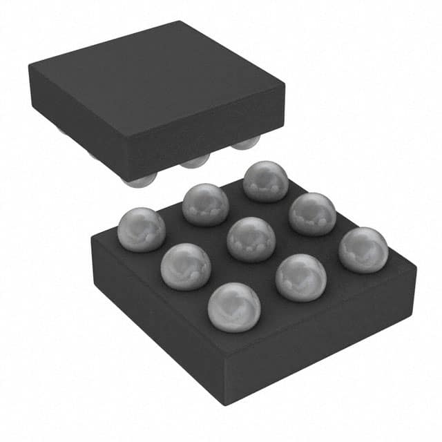
| 产品图片 |
|
| rohs | 符合RoHS无铅 / 符合限制有害物质指令(RoHS)规范要求 |
| 产品系列 | 音频 IC,音频放大器,Maxim Integrated MAX98314EWL+T- |
| 数据手册 | |
| 产品型号 | MAX98314EWL+T |
| Pd-功率耗散 | 851 mW |
| THD+噪声 | 0.03 % |
| 不同负载时的最大输出功率x通道数 | 3.2W x 1 @ 4 欧姆 |
| 产品 | Audio Amplifiers |
| 产品种类 | 音频放大器 |
| 供应商器件封装 | 9-WLP (.96x.96) |
| 共模抑制比—最小值 | 67 dB |
| 其它名称 | MAX98314EWL+TCT |
| 包装 | 剪切带 (CT) |
| 商标 | Maxim Integrated |
| 安装类型 | 表面贴装 |
| 安装风格 | SMD/SMT |
| 封装 | Reel |
| 封装/外壳 | 9-WFBGA,WLBGA |
| 封装/箱体 | WLP-9 |
| 工作温度 | -40°C ~ 85°C (TA) |
| 工作电源电压 | 2.5 V to 5.5 V |
| 工厂包装数量 | 2500 |
| 应用说明 | |
| 最大功率耗散 | 851 mW |
| 最大工作温度 | + 85 C |
| 最小工作温度 | - 40 C |
| 标准包装 | 1 |
| 特性 | 消除爆音,差分输入,短路和热保护,关闭 |
| 特色产品 | http://www.digikey.cn/product-highlights/zh/MAX98314-Mono-32-W-Class-D-Amplifier-with-Integrated-Input-Coupling-Capacitors/52441 |
| 电压-电源 | 2.5 V ~ 5.5 V |
| 电源电流 | 1.2 mA |
| 类 | Class-D |
| 类型 | 1-Channel Mono |
| 系列 | MAX98314 |
| 输出功率 | 3.2 W x 1 at 4 Ohms |
| 输出类型 | 1-通道(单声道) |
| 零件号别名 | MAX98314 |


PDF Datasheet 数据手册内容提取
19-6124; Rev 0; 11/11 EVALUATION KIT AVAILABLE MAX98314 Mono 3.2W Class D Amplifier with Integrated Input Coupling Capacitors General Description Features The MAX98314 mono 3.2W Class D amplifier provides S Integrated Input Coupling Capacitors with Class AB audio performance with Class D efficiency. Excellent Linearity This device offers five selectable gain settings (0dB, fC = 100Hz (6dB) 3dB, 6dB, 9dB, and 12dB) set by a single gain-select fC = 200Hz (12dB) input (GAIN). S Low Quiescent Current Active emissions limiting (AEL) edge rate and overshoot 0.95mA at 3.7V control circuitry and a filterless spread-spectrum modu- 1.2mA at 5.0V lation (SSM) scheme greatly reduce EMI and eliminate S Delivers High Output Power at 10% THD+N the need for output filtering found in traditional Class D 3.2W into 4I, VPVDD = 5V devices. 960mW into 8I, VPVDD = 3.7V The IC’s low 0.95mA at 3.7V, 1.2mA at 5.0V quiescent S Ultra-Low Noise: 19µV current extends battery life in portable applications. S Eliminates Output Filtering Requirement Highly linear, integrated input coupling capacitors (CIN) Spread Spectrum and Active Emissions Limiting reduce solution size and provide excellent THD+N, PSRR, S Click-and-Pop Suppression and CMRR performance at low frequencies vs. standard Class D amplifiers using external input capacitors. S Thermal and Overcurrent Protection The IC is available in a small 9-bump, 0.3mm pitch WLP S Low Current Shutdown Mode (1.0mm x 1.0mm x 0.80mm) package and is specified S Small, Space-Saving Package over the -40NC to +85NC extended temperature range. Applications Simplified Block Diagram Mobile Phones Portable Audio Notebook Computers MAX98314 CIN MP3 Players CLASS D Netbook Computers MODULATOR CIN AND H-BRIDGE VoIP Phones GAIN CONTROL Ordering Information appears at end of data sheet. For related parts and recommended products to use with this part, refer to: www.maxim-ic.com/MAX98314.related ����������������������������������������������������������������� Maxim Integrated Products 1 For pricing, delivery, and ordering information, please contact Maxim Direct at 1-888-629-4642, or visit Maxim’s website at www.maxim-ic.com.
MAX98314 Mono 3.2W Class D Amplifier with Integrated Input Coupling Capacitors Functional Diagram/Typical Application Circuit 2.5V TO 5.5V 0.1µF 10µF* PVDD A3 SHDN C1 UVLO/POWER CLICK-AND-POP MANAGEMENT SUPPRESSION PVDD MAX98314 GAIN B3 LOW-EMI A1 OUT- DRIVER C3 IN+ PGND CLASS D MODULATOR PVDD C2 IN- LOW-EMI A2 OUT+ DRIVER PGND B1 PGND *SYSTEM BULK CAPACITANCE. ����������������������������������������������������������������� Maxim Integrated Products 2
MAX98314 Mono 3.2W Class D Amplifier with Integrated Input Coupling Capacitors ABSOLUTE MAXIMUM RATINGS PVDD, IN+, IN-, SHDN, GAIN to PGND ...................0.3V to +6V Continuous Power Dissipation (TA = +70NC) for Multilayer Board OUT+, OUT- to PGND ............................0.3V to (VPVDD + 0.3V) WLP (derate 10.64mW/NC above +70NC) .....................851mW Continuous Current In/Out of PVDD, PGND, OUT_ .........750mA Junction Temperature .....................................................+150NC Continuous Input Current (all other pins) ........................Q20mA Operating Temperature Range ..........................-40NC to +85NC Duration of Short Circuit Between Storage Temperature Range ............................-65NC to +150NC OUT_ to PVDD, PGND ..........................................Continuous Soldering Temperature (reflow) ......................................+260NC Between OUT+ and OUT- Pins .............................Continuous Stresses beyond those listed under “Absolute Maximum Ratings” may cause permanent damage to the device. These are stress ratings only, and functional opera- tion of the device at these or any other conditions beyond those indicated in the operational sections of the specifications is not implied. Exposure to absolute maximum rating conditions for extended periods may affect device reliability. PACKAGE THERMAL CHARACTERISTICS (Note 1) WLP Junction-to-Ambient Thermal Resistance (BJA) ........102NC/W Junction-to-Case Thermal Resistance (BJC) ...............47NC/W Note 1: Package thermal resistances were obtained using the method described in JEDEC specification JESD51-7, using a four- layer board. For detailed information on package thermal considerations, refer to www.maxim-ic.com/thermal-tutorial. ELECTRICAL CHARACTERISTICS (VPVDD = VSHDN = VGAIN = 5V, VPGND = 0V, AV = 6dB (GAIN = PVDD), RL = J, RL connected between OUT+ to OUT-, AC measure- ment bandwidth 20Hz to 22kHz, TA = TMIN to TMAX, unless otherwise noted. Typical values are at TA = +25NC.) (Note 2, 3) PARAMETER SYMBOL CONDITIONS MIN TYP MAX UNITS AMPLIFIER CHARACTERISTICS Supply Voltage Range VPVDD Guaranteed by PSRR test 2.5 5.5 V Undervoltage Lockout UVLO PVDD falling 1.8 2.2 V VPVDD = 5V 1.2 1.8 Quiescent Current IPVDD mA VPVDD = 3.7V 0.95 Shutdown Supply Current ISHDN VSHDN = 0V, TA = +25NC < 0.1 10 FA Turn-On Time tON 3.7 10 ms Bias Voltage VBIAS VPVDD/2 V GAIN connected to PGND 11.75 12 12.25 GAIN connected to PGND 8.75 9 9.25 through 100kI Q5% resistor Voltage Gain AV f = 1kHz GAIN connected to PVDD 5.75 6 6.25 dB GAIN connected to PVDD 2.75 3 3.25 through 100kI Q5% resistor GAIN unconnected -0.25 0 +0.25 Input Capacitance CIN All gains 0.011 FF AV = 12dB 199 AV = 9dB 139 Highpass Corner Frequency fC -3dB down AV = 6dB 63 100 189 Hz AV = 3dB 70 AV = 0dB 50 ����������������������������������������������������������������� Maxim Integrated Products 3
MAX98314 Mono 3.2W Class D Amplifier with Integrated Input Coupling Capacitors ELECTRICAL CHARACTERISTICS (continued) (VPVDD = VSHDN = VGAIN = 5V, VPGND = 0V, AV = 6dB (GAIN = PVDD), RL = J, RL connected between OUT+ to OUT-, AC measure- ment bandwidth 20Hz to 22kHz, TA = TMIN to TMAX, unless otherwise noted. Typical values are at TA = +25NC.) (Note 2, 3) PARAMETER SYMBOL CONDITIONS MIN TYP MAX UNITS Common-Mode Rejection Ratio CMRR fIN = 1kHz, input referred 67 dB Output Offset Voltage VOS TA = +25NC (Note 4) Q1 Q3 mV RL = 8I + 68FH, peak Into shutdown -59 voltage, TA = +25NC, Click-and-Pop Level KCP A-weighted, 32 dBV samples per second, Out of shutdown -82 TA = +25NC (Notes 4, 5) VPVDD = 2.5V to 5.5V, TA = +25NC 70 90 Power-Supply Rejection Ratio f = 217Hz 74 PSRR dB (Note 4) VRIPPLE = 200mVP-P f = 1kHz 72 f = 20kHz 49 THD+N = 10% VPVDD = 5.0V 3.2 f = 1kHz VPVDD = 4.2V 2.2 RL = 4I + 33FH VPVDD = 3.7V 1.7 THD+N = 1% VPVDD = 5.0V 2.6 f = 1kHz VPVDD = 4.2V 1.8 RL = 4I + 33FH VPVDD = 3.7V 1.4 Output Power POUT THD+N = 10% VPVDD = 5.0V 1.8 W f = 1kHz VPVDD = 4.2V 1.2 RL = 8I + 68FH VPVDD = 3.7V 0.96 THD+N = 1% VPVDD = 5.0V 1.4 f = 1kHz VPVDD = 4.2V 1 RL = 8I + 68FH VPVDD = 3.7V 0.8 RL = 4I, 0.03 0.1 Total Harmonic Distortion Plus POUT = 1W Noise THD+N fIN = 1kHz RL = 8I 0.03 % POUT = 0.725W AV = 12dB 31 AV = 9dB 26 Output Noise VN A-weighted (Note 4) AV = 6dB 23 FVRMS AV = 3dB 21 AV = 0dB 19 Efficiency E RL = 8I, POUT = 1.8W, f = 1kHz 93 % Oscillator Frequency fOSC 300 kHz Spread-Spectrum Bandwidth 20 kHz Current Limit 2.8 A Thermal Shutdown Level 155 NC ����������������������������������������������������������������� Maxim Integrated Products 4
MAX98314 Mono 3.2W Class D Amplifier with Integrated Input Coupling Capacitors ELECTRICAL CHARACTERISTICS (continued) (VPVDD = VSHDN = VGAIN = 5V, VPGND = 0V, AV = 6dB (GAIN = PVDD), RL = J, RL connected between OUT+ to OUT-, AC measure- ment bandwidth 20Hz to 22kHz, TA = TMIN to TMAX, unless otherwise noted. Typical values are at TA = +25NC.) (Note 2, 3) PARAMETER SYMBOL CONDITIONS MIN TYP MAX UNITS Thermal Hysteresis 15 NC DIGITAL INPUT (SHDN) Input Voltage High VINH VPVDD = 2.5V to 5.5V 1.4 V Input Voltage Low VINL VPVDD = 2.5V to 5.5V 0.4 V Input Leakage Current TA = +25NC Q1 FA Note 2: All devices are 100% production tested at TA = +25NC. Specifications over temperature limits are guaranteed by design. Note 3: Testing performed with a resistive load in series with an inductor to simulate an actual speaker load. For RL = 4I, L = 33FH. For RL = 8I, L = 68FH. Note 4: Amplifier inputs AC-coupled to ground. Note 5: Mode transitions controlled by SHDN control pin. Typical Operating Characteristics (VPVDD = VSHDN = 5.0V, VPGND = 0V, AV = 6dB, RL = J, RL connected between OUT+ to OUT-, AC measurement bandwidth 20Hz to 22kHz, TA = +25NC, unless otherwise noted.) TOTAL HARMONIC DISTORTION PLUS TOTAL HARMONIC DISTORTION PLUS TOTAL HARMONIC DISTORTION PLUS NOISE vs. FREQUENCY NOISE vs. FREQUENCY NOISE vs. FREQUENCY 10 10 10 1 ZVLPOVADDD == 45IV + 33µH MAX98314 toc01 1 ZVLPOVADDD == 44I.2 V+ 33µH POUT = 1W MAX98314 toc02 1 ZVLPOVADDD == 43I.7 V+ 33µH POUT = 0.8W MAX98314 toc03 POUT = 2W %) %) %) +N ( 0.1 +N ( 0.1 +N ( 0.1 HD POUT = 1.5W HD HD T T T 0.01 0.01 0.01 POUT = 0.5W POUT = 0.2W 0.001 0.001 0.001 10 100 1k 10k 100k 10 100 1k 10k 100k 10 100 1k 10k 100k FREQUENCY (Hz) FREQUENCY (Hz) FREQUENCY (Hz) TOTAL HARMONIC DISTORTION PLUS TOTAL HARMONIC DISTORTION PLUS TOTAL HARMONIC DISTORTION PLUS NOISE vs. FREQUENCY NOISE vs. FREQUENCY NOISE vs. FREQUENCY 10 10 10 1 ZVLPOVADDD == 85IV + 68µPHOUT = 1.2W MAX98314 toc04 1 ZVLPOVADDD == 84I.2 V+ 68µHPOUT = 0.6W MAX98314 toc05 1 ZVLPOVADDD == 83I.7 V+ 68µH POUT = 0.4W MAX98314 toc06 %) %) %) +N ( 0.1 +N ( 0.1 +N ( 0.1 D D D H H H T T T POUT = 0.2W 0.01 0.01 0.01 POUT = 0.2W POUT = 0.3W 0.001 0.001 0.001 10 100 1k 10k 100k 10 100 1k 10k 100k 10 100 1k 10k 100k FREQUENCY (Hz) FREQUENCY (Hz) FREQUENCY (Hz) ����������������������������������������������������������������� Maxim Integrated Products 5
MAX98314 Mono 3.2W Class D Amplifier with Integrated Input Coupling Capacitors Typical Operating Characteristics (continued) (VPVDD = VSHDN = 5.0V, VPGND = 0V, AV = 6dB, RL = J, RL connected between OUT+ to OUT-, AC measurement bandwidth 20Hz to 22kHz, TA = +25NC, unless otherwise noted.) TOTAL HARMONIC DISTORTION PLUS TOTAL HARMONIC DISTORTION PLUS TTOOTTAALL HHAARRMMOONNIICC DDIISSTTOORRTTIIOONN PPLLUUSS NOISE vs. OUTPUT POWER NOISE vs. OUTPUT POWER NNOOIISSEE vvss.. OOUUTTPPUUTT PPOOWWEERR 100 100 100 10 ZVLPOVADDD == 45IV + 33µH MAX98314 toc07 10 ZVLPOVADDD == 44I.2 V+ 33µH MAX98314 toc08 10 ZVLPOVADDD == 43I.7 V+ 33µH MAX98314 toc09 %) 1 f = 6kHz %) 1 f = 6kHz %) 1 f = 6kHz N ( N ( N ( THD+ 0.1 f = 1kHz THD+ 0.1 f = 1kHz THD+ 0.1 f = 1kHz 0.01 0.01 0.01 f = 100Hz f = 100Hz f = 100Hz 0.001 0.001 0.001 0 0.5 1.0 1.5 2.0 2.5 3.0 3.5 4.0 0 0.5 1.0 1.5 2.0 2.5 0 0.5 1.0 1.5 2.0 OUTPUT POWER (W) OUTPUT POWER (W) OUTPUT POWER (W) TTOOTTAALL HHAARRMMOONNIICC DDIISSTTOORRTTIIOONN PPLLUUSS TOTAL HARMONIC DISTORTION PLUS TOTAL HARMONIC DISTORTION PLUS NNOOIISSEE vvss.. OOUUTTPPUUTT PPOOWWEERR NOISE vs. OUTPUT POWER NOISE vs. OUTPUT POWER 100 100 100 10 ZVLPOVADDD == 85IV + 68µH MAX98314 toc10 10 ZVLPOVADDD == 84I.3 V+ 68µH MAX98314 toc11 10 ZVLPOVADDD == 83I.7 V+ 68µH MAX98314 toc12 %) 1 f = 6kHz %) 1 f = 6kHz %) 1 f = 6kHz N ( N ( N ( THD+ 0.1 f = 1kHz THD+ 0.1 f = 1kHz THD+ 0.1 f = 1kHz 0.01 0.01 0.01 f = 100Hz f = 100Hz f = 100Hz 0.001 0.001 0.001 0 0.5 1.0 1.5 2.0 0 0.3 0.6 0.9 1.2 1.5 0 0.3 0.6 0.9 1.2 OUTPUT POWER (W) OUTPUT POWER (W) OUTPUT POWER (W) OUTPUT POWER vs. LOAD RESISTANCE OUTPUT POWER vs. LOAD RESISTANCE OUTPUT POWER vs. SUPPLY VOLTAGE 344...505 VPVDD = 5V MAX98314 toc13 22..05 VPVDD = 3.7V MAX98314 toc14 344...505 fZ =LO 1AkDH =z 4I + 33µH MAX98314 toc15 WER (W) 23..50 THD+N = 10% WER (W) 1.5 WER (W) 23..50 THD+N = 10% O O O P P P UT 2.0 UT UT 2.0 OUTP 1.5 OUTP 1.0 THD+N = 10% OUTP 1.5 THD+N = 1% 1.0 0.5 THD+N = 1% 1.0 0.5 THD+N = 1% 0.5 0 0 0 1 10 100 1000 1 10 100 1000 2.5 3.0 3.5 4.0 4.5 5.0 5.5 RLOAD (I) RLOAD (I) SUPPLY VOLTAGE (V) ����������������������������������������������������������������� Maxim Integrated Products 6
MAX98314 Mono 3.2W Class D Amplifier with Integrated Input Coupling Capacitors Typical Operating Characteristics (continued) (VPVDD = VSHDN = 5.0V, VPGND = 0V, AV = 6dB, RL = J, RL connected between OUT+ to OUT-, AC measurement bandwidth 20Hz to 22kHz, TA = +25NC, unless otherwise noted.) OUTPUT POWER vs. SUPPLY VOLTAGE GAIN vs. FREQUENCY EFFICIENCY vs. OUTPUT POWER 22..05 fZ =LO 1AkDH =z 8I + 68µH MAX98304 toc16 112050 GAIN = 9dB GAIN = 12dB MAX98314 toc17 1890000 VPVDD = 5V MAX98314 toc18 W) 70 ZLOAD = 8I + 68µH OUTPUT POWER ( 11..05 THD+N = 10% GAIN (dB) -505 GAIN = 0dB GAIN = 3dBGAIN = 6dB EFFICIENCY (%) 34560000 ZLOAD = 4I + 33µH THD+N = 1% -10 0.5 20 -15 10 0 -20 0 2.5 3.0 3.5 4.0 4.5 5.0 5.5 10 100 1k 10k 100k 0 0.5 1.0 1.5 2.0 2.5 3.0 3.5 SUPPLY VOLTAGE (V) FREQUENCY (Hz) OUTPUT POWER (W) SUPPLY CURRENT POWER-SUPPLY REJECTION EFFICIENCY vs. OUTPUT POWER vs. SUPPLY VOLTAGE RATIO vs. FREQUENCY 1890000 VPVDD = 3.7V MAX98314 toc19 112...680 MAX98314 toc20 1890000 VZLROIPAPDL E= =8 I20 0+m 6V8µPH-P MAX98314 toc21 EFFICIENCY (%) 45670000 ZLOAD = 8I + 68µH ZLOAD = 4I + 33µH PPLY CURRENT (mA) 0111....8024 PSRR (dB) 45670000 30 SU 0.6 30 20 0.4 20 10 0.2 10 0 0 0 0 0.5 1.0 1.5 2.0 2.5 3.0 3.5 4.0 4.5 5.0 5.5 10 100 1k 10k 100k OUTPUT POWER (W) SUPPLY VOLTAGE (V) FREQUENCY (Hz) POWER-SUPPLY REJECTION COMMON-MODE REJECTION RATIO RATIO vs. SUPPLY VOLTAGE vs. FREQUENCY 0 120 --2100 fV =R I1PkPHLEz = 200mVP-P MAX98314 toc22 11901000 ZLOAD = 8I +A 6V8 =µ H9dB MAX98314 toc23 -30 80 AV = 12dB AV = 6dB SRR (dB) --5400 MRR (dB) 6700 P -60 C 4500 AV = 3dB AV = 0dB -70 30 -80 20 -90 10 -100 0 2.5 3.0 3.5 4.0 4.5 5.0 5.5 10 100 1k 10k 100k SUPPLY VOLTAGE (V) FREQUENCY (Hz) ����������������������������������������������������������������� Maxim Integrated Products 7
MAX98314 Mono 3.2W Class D Amplifier with Integrated Input Coupling Capacitors Typical Operating Characteristics (continued) (VPVDD = VSHDN = 5.0V, VPGND = 0V, AV = 6dB, RL = J, RL connected between OUT+ to OUT-, AC measurement bandwidth 20Hz to 22kHz, TA = +25NC, unless otherwise noted.) STARTUP RESPONSE SHUTDOWN RESPONSE MAX98314 toc24 MAX98314 toc25 VSHDN 2V/div VSHDN 2V/div ISPKR_OUT ISPKR_OUT 100mA/div 100mA/div 1ms/div WIDEBAND vs. FREQUENCY NARROWBAND vs. FREQUENCY DE (dBV) --42000 RBW = 100Hz MAX98314 toc26 DE (dBV) --42000 fV =O U1Tk H=z -60dBV MAX98314 toc27 GNITU -60 GNITU -60 MA MA -80 UTPUT -80 UTPUT -100 O O -100 -120 -120 -140 0.1 1 10 100 10 100 1k 10k 100k FREQUENCY (MHz) FREQUENCY (Hz) ����������������������������������������������������������������� Maxim Integrated Products 8
MAX98314 Mono 3.2W Class D Amplifier with Integrated Input Coupling Capacitors Pin Configuration TOP VIEW (BUMP-SIDE DOWN) MAX98314 1 2 3 + A OUT- OUT+ PVDD B PGND N.C. GAIN C SHDN IN- IN+ WLP (0.3mm pitch) Pin Description BUMP NAME FUNCTION A1 OUT- Negative Speaker Output A2 OUT+ Positive Speaker Output A3 PVDD Power Supply. Bypass PVDD with a 0.1FF and 10FF capacitor to PGND. B1 PGND Power Ground B2 N.C. No Connection. Can be left unconnected or connected to PGND. B3 GAIN Gain Select. See Table 1 for GAIN settings. C1 SHDN Active-Low Shutdown Input. Drive SHDN low to place the device in shutdown. C2 IN- Inverting Audio Input C3 IN+ Noninverting Audio Input ����������������������������������������������������������������� Maxim Integrated Products 9
MAX98314 Mono 3.2W Class D Amplifier with Integrated Input Coupling Capacitors Detailed Description Amplifier Current Limit If the output current of the speaker amplifier exceeds the The MAX98314 features low quiescent current, a low- current limit (2.8A typ), the IC disables the outputs for power shutdown mode, comprehensive click-and-pop approximately 100Fs. At the end of 100Fs, the outputs suppression, and excellent RF immunity. are reenabled. If the fault condition still exists, the IC continues to disable and reenable the outputs until the The IC offers Class AB audio performance with Class D fault condition is removed. efficiency in a minimal board-space solution. The Class D amplifier features spread-spectrum modulation, edge- Selectable Amplifier Gain rate, and overshoot control circuitry that offers significant The IC offers five programmable gain settings, selectable improvements to switch-mode amplifier radiated emis- by a single gain input (GAIN). sions. The amplifier features click-and-pop suppression that Table 1. GAIN Selection reduces audible transients on startup and shutdown. The amplifier additionally includes thermal overload and GAIN PIN MAXIMUM GAIN (dB) short-circuit protection. Connect to PGND 12 Highly linear, integrated input coupling capacitors (CIN) Connect to PGND through 9 reduce solution size and provide excellent THD+N, 100kI Q5% PSRR, and CMRR performance at low frequencies vs. Connect to PVDD 6 standard Class D amplifiers using external input capaci- Connect to PVDD through tors. 3 100kI Q5% Class D Speaker Amplifier Unconnected 0 The IC’s filterless Class D amplifier offers much higher efficiency than Class AB amplifiers. The high efficiency of a Class D amplifier is due to the switching operation of Integrated Input Coupling Capacitors (CIN) The IC integrates two 0.011FF input coupling capacitors, the output stage transistors. Any power loss associated with the Class D output stage is mostly due to the I2R loss CIN. The input coupling capacitors, in conjunction with of the MOSFET on-resistance and quiescent switching the amplifier’s internal input resistance (RIN), form a first- order highpass filter that removes the DC bias from the current overhead. incoming signal. These capacitors allow the amplifier to Ultra-Low EMI Filterless Output Stage bias the signal to an optimum DC level. Traditional Class D amplifiers require the use of external LC filters, or shielding, to meet electromagnetic inter- ference (EMI) regulation standards. Maxim’s patented 90 active emissions limiting edge-rate control circuitry and spread-spectrum modulation reduces EMI emissions, 70 while maintaining up to 93% efficiency. V/m) µ B The spread-spectrum modulation mode flattens wide- L (d 50 band spectral components, while proprietary techniques VE EN5502B LIMIT E L ensure that the cycle-to-cycle variation of the switching NS 30 O period does not degrade audio reproduction or effi- SI HORIZONTAL S ciency. The IC’s spread-spectrum modulator randomly MI E 10 varies the switching frequency by Q20kHz around the center frequency (300kHz). Above 10MHz, the wideband VERTICAL -10 spectrum looks like noise for EMI purposes (Figure 1). 0 100 200300 400 500 600 700800 9001000 FREQUENCY (MHz) Figure 1. EMI Performance with 60cm of Speaker Cable, No Output Filter ���������������������������������������������������������������� Maxim Integrated Products 10
MAX98314 Mono 3.2W Class D Amplifier with Integrated Input Coupling Capacitors Assuming zero source impedance, the -3dB corner Applications Information frequency, f-3dB, is: f-3dB = 1/2GRINCIN [Hz] Filterless Class D Operation Traditional Class D amplifiers require an output filter. The 100ppm/V voltage coefficient of the integrated input The filter adds cost and size, and decreases efficiency coupling capacitor results in excellent low-frequency and THD+N performance. The IC’s filterless modulation THD+N performance. Figure 2 illustrates the superior scheme does not require an output filter. linearity of the IC’s integrated input coupling capacitors compared to a similar amplifier with external 0.01FF X7R Because the switching frequency of the IC is well beyond and X5R 0402 input coupling capacitors. the bandwidth of most speakers, voice coil movement due to the switching frequency is very small. Use a TOTAL HARMONIC DISTORTION speaker with a series inductance > 10FH. Typical 8I PLUS NOISE vs. FREQUENCY speakers exhibit series inductances in the 20FH to 10 100FH range. VPVDD = 4.2V ZLOAD = 8I + 68µH Speaker Amplifier Power-Supply Input (PVDD) POUT = 600mW 1.0 PVDD powers the speaker amplifier and ranges from X7R CAPS 2.5V to 5.5V. Bypass PVDD with a 0.1FF and 10FF %) capacitor to PGND. Apply additional bulk capacitance D+N ( 0.1 X5R CAPS at the device if long input traces between PVDD and the H T power source are used. 0.01 Layout and Grounding Proper layout and grounding are essential for optimum MAX98314 INTERNAL CAPS performance. Good grounding improves audio perfor- 0.001 mance and prevents switching noise from coupling into 10 100 1k 10k 100k the audio signal. FREQUENCY (Hz) Use wide, low-resistance output traces. As the load Figure 2. Low-Frequency THD+N Performance impedance decreases, the current drawn from the device increases. At higher current, the resistance of the output traces decrease the power delivered to the load. Shutdown For example, if 2W is delivered from the device output to The IC features a low-power shutdown mode, drawing a 4I load through 100mI of total speaker trace, 1.904W < 0.1FA (typ) of supply current. Drive SHDN low to put is delivered to the speaker. If power is delivered through the IC into shutdown. 10mI of total speaker trace, 1.99W is delivered to the Click-and-Pop Suppression speaker. Wide output, supply, and ground traces also The speaker amplifier features Maxim’s comprehensive improve the power dissipation of the device. click-and-pop suppression. During startup, the click- The IC is inherently designed for excellent RF immunity. and-pop suppression circuitry reduces any audible For best performance, add ground fills around all signal transient sources internal to the device. When entering traces on top or bottom PCB layers. shutdown, the differential speaker outputs ramp down to PGND quickly and simultaneously. ���������������������������������������������������������������� Maxim Integrated Products 11
MAX98314 Mono 3.2W Class D Amplifier with Integrated Input Coupling Capacitors WLP Applications Information For the latest application details on WLP construction, 0.18mm dimensions, tape carrier information, PCB techniques, bump-pad layout, and recommended reflow temperature profile, as well as the latest information on reliability test- ing results, refer to Application Note 1891: Wafer-Level Packaging (WLP) and Its Applications. Figure 3 shows the dimensions of the WLP balls used on the IC. Ordering Information 0.18mm PART TEMP RANGE PIN-PACKAGE MAX98314EWL+ -40NC to +85NC 9 WLP Figure 3. WLP Ball Dimensions +Denotes a lead(Pb)-free/RoHS-compliant package. ���������������������������������������������������������������� Maxim Integrated Products 12
MAX98314 Mono 3.2W Class D Amplifier with Integrated Input Coupling Capacitors Package Information For the latest package outline information and land patterns (footprints), go to www.maxim-ic.com/packages. Note that a “+”, “#”, or “-” in the package code indicates RoHS status only. Package drawings may show a different suffix character, but the drawing pertains to the package regardless of RoHS status. PACKAGE TYPE PACKAGE CODE OUTLINE NO. LAND PATTERN NO. Refer to 9 WLP (0.3mm pitch) W90A0+1 21-0539 Application Note 1891 COMMON DIMENSIONS PIN 1 E MARKING A 0.75 0.05 INDICATOR A3 A1 0.16 0.03 1 A2 0.59 REF A A3 0.040 BASIC A1 AAAA D A2 A b 0.21 0.03 D1 0.60 BASIC 0.05 S E1 0.60 BASIC S SNeoete 7 e 0.30 BASIC SD 0.00 BASIC TOP VIEW SIDE VIEW SE 0.00 BASIC E D DEPOPULATED PKG. CODE MIN MAX MIN MAX BUMPS W90A0+1 0.95 0.980.95 0.98 NONE E1 SE e NOTES: B SD 1. Terminal pitch is defined by terminal center to center value. C 2. Outer dimension is defined by center lines between scribe lines. 3. All dimensions in millimeter. B D1 4. Marking shown is for package orientation reference only. 5. Tolerance is ± 0.02 unless specified otherwise. A 6. All dimensions apply to PbFree (+) package codes only. 7. Front - side finish can be either Black or Clear. 1 2 3 b A BOTTOM VIEW TITLE Package Outline 9 bumps, WLP Pkg. 0.3MM Pitch -DRAWING NOT TO SCALE- APPROVAL DOCUMENT CONTROL NO. REV. 1 21-0539 B 1 ���������������������������������������������������������������� Maxim Integrated Products 13
MAX98314 Mono 3.2W Class D Amplifier with Integrated Input Coupling Capacitors Revision History REVISION REVISION PAGES DESCRIPTION NUMBER DATE CHANGED 0 11/11 Initial release — Maxim cannot assume responsibility for use of any circuitry other than circuitry entirely embodied in a Maxim product. No circuit patent licenses are implied. Maxim reserves the right to change the circuitry and specifications without notice at any time. The parametric values (min and max limits) shown in the Electrical Characteristics table are guaranteed. Other parametric values quoted in this data sheet are provided for guidance. Maxim Integrated Products, 120 San Gabriel Drive, Sunnyvale, CA 94086 408-737-7600 14 © 2011 Maxim Integrated Products Maxim is a registered trademark of Maxim Integrated Products, Inc.