ICGOO在线商城 > 集成电路(IC) > 线性 - 音頻放大器 > LME49610TS/NOPB

 Datasheet下载
- 型号: LME49610TS/NOPB
- 制造商: Texas Instruments
- 库位|库存: xxxx|xxxx
- 要求:
| 数量阶梯 | 香港交货 | 国内含税 |
| +xxxx | $xxxx | ¥xxxx |
查看当月历史价格
查看今年历史价格
LME49610TS/NOPB产品简介:
ICGOO电子元器件商城为您提供LME49610TS/NOPB由Texas Instruments设计生产,在icgoo商城现货销售,并且可以通过原厂、代理商等渠道进行代购。 LME49610TS/NOPB价格参考。Texas InstrumentsLME49610TS/NOPB封装/规格:线性 - 音頻放大器, Amplifier IC 1-Channel (Mono) Class AB DDPAK/TO-263-5。您可以下载LME49610TS/NOPB参考资料、Datasheet数据手册功能说明书,资料中有LME49610TS/NOPB 详细功能的应用电路图电压和使用方法及教程。
Texas Instruments(德州仪器)的LME49610TS/NOPB是一款高性能、低失真、低噪声的音频运算放大器,适用于多种高保真音频应用场景。以下是其主要应用场景:

 1. 高端音响系统
LME49610TS/NOPB具有极低的总谐波失真(THD+N),能够提供纯净的音频信号,特别适合用于高端家用音响系统和专业音频设备中。它可以在不损失音质的情况下放大微弱的音频信号,确保输出的声音清晰、细腻,适合对音质要求极高的用户。

 2. 耳机放大器
该器件的低噪声特性使其非常适合用于耳机放大器的设计。无论是便携式耳机放大器还是台式耳机放大器,LME49610TS/NOPB都能提供出色的音质表现,尤其在驱动高阻抗耳机时,能够保持稳定的输出和优秀的动态范围。

 3. 录音设备
在录音棚或现场录音设备中,LME49610TS/NOPB可以作为前置放大器使用。它的低噪声和高线性度有助于捕捉更真实的音频信号,减少背景噪音的干扰,确保录音质量达到专业水平。

 4. 汽车音响系统
对于汽车音响系统,LME49610TS/NOPB的高可靠性和宽工作温度范围使其成为理想选择。它可以承受汽车环境中的温度变化,并且能够在有限的空间内提供高质量的音频输出,提升车内听觉体验。

 5. 便携式音频设备
在便携式音频播放器、移动扬声器等小型设备中,LME49610TS/NOPB的低功耗特性有助于延长电池寿命,同时保持出色的音质表现。其紧凑的封装形式也便于集成到各种便携式设备中。

 6. 医疗音频设备
在某些医疗设备中,如超声波成像仪或听力测试设备,音频信号的准确性至关重要。LME49610TS/NOPB的低失真和高精度特性可以确保这些设备的音频信号处理更加准确,从而提高诊断和治疗的效果。

总之,LME49610TS/NOPB凭借其卓越的性能,广泛应用于需要高保真音频放大的场合,尤其是在对音质有严格要求的专业领域。
| 参数 | 数值 |
| 产品目录 | 集成电路 (IC)半导体 |
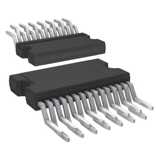
| 描述 | IC AUDIO BUFFER 250MA TO263-5音频放大器 Hi Perf Hi Fidelity Hi Crnt Audio Buffer |
| 产品分类 | |
| 品牌 | Texas Instruments |
| 产品手册 | |
| 产品图片 |
|
| rohs | 符合RoHS含铅 / 不受限制有害物质指令(RoHS)规范要求限制 |
| 产品系列 | 音频 IC,音频放大器,Texas Instruments LME49610TS/NOPB- |
| 数据手册 | |
| 产品型号 | LME49610TS/NOPB |
| THD+噪声 | 0.00003 % |
| 不同负载时的最大输出功率x通道数 | 500mW x 1 @ 32 欧姆 |
| 产品 | General Purpose Audio Amplifiers |
| 产品目录页面 | |
| 产品种类 | 音频放大器 |
| 供应商器件封装 | DDPAK/TO-263-5 |
| 其它名称 | *LME49610TS/NOPB |
| 包装 | 管件 |
| 双重电源电压 | +/- 3 V, +/- 5 V, +/- 9 V, +/- 12 V, +/- 15 V, +/- 18 V |
| 商标 | Texas Instruments |
| 安装类型 | 表面贴装 |
| 安装风格 | SMD/SMT |
| 封装 | Tube |
| 封装/外壳 | TO-263-6,D²Pak(5 引线+接片),TO-263BA |
| 封装/箱体 | TO-263-5 |
| 工作温度 | -40°C ~ 85°C (TA) |
| 工作电源电压 | 2.25 V to 22 V |
| 工厂包装数量 | 45 |
| 最大功率耗散 | 500 mW |
| 最大工作温度 | + 85 C |
| 最小工作温度 | - 40 C |
| 标准包装 | 45 |
| 特性 | 短路和热保护 |
| 电压-电源 | ±2.25 V ~ 22 V |
| 电源电流 | 13 mA |
| 类型 | AB 类 |
| 系列 | LME49610 |
| 输出类型 | 1-通道(单声道) |


- 商务部:美国ITC正式对集成电路等产品启动337调查
- 曝三星4nm工艺存在良率问题 高通将骁龙8 Gen1或转产台积电
- 太阳诱电将投资9.5亿元在常州建新厂生产MLCC 预计2023年完工
- 英特尔发布欧洲新工厂建设计划 深化IDM 2.0 战略
- 台积电先进制程称霸业界 有大客户加持明年业绩稳了
- 达到5530亿美元!SIA预计今年全球半导体销售额将创下新高
- 英特尔拟将自动驾驶子公司Mobileye上市 估值或超500亿美元
- 三星加码芯片和SET,合并消费电子和移动部门,撤换高东真等 CEO
- 三星电子宣布重大人事变动 还合并消费电子和移动部门
- 海关总署:前11个月进口集成电路产品价值2.52万亿元 增长14.8%


PDF Datasheet 数据手册内容提取
LME49610 www.ti.com SNAS435B–APRIL2008–REVISEDAPRIL2013 LME49610 High Performance, High Fidelity, High Current Audio Buffer CheckforSamples:LME49610 FEATURES DESCRIPTION 1 • Pin-SelectableBandwidthandQuiescent The LME49610 is a high performance, low distortion 2 high fidelity 250mA audio buffer. The LME49610 is Current designedforawiderangeofapplications.Whenused • PureFidelity.PurePerformance inside the feedback loop of an op amp, it increases • ShortCircuitProtection output current, improves capacitive load drive, and • ThermalShutdown eliminatesthermalfeedback. • TO–263Surface-MountPackage The LME49610 offers a pin-selectable bandwidth: a low current, 120MHz bandwidth mode that consumes APPLICATIONS 13mA and a wide 200MHz bandwidth mode that consumes 19mA. In both modes the LME49610 has • HeadphoneAmplifierOutputDriveStage a nominal 2000V/μs slew rate. Bandwidth is easily • LineDrivers adjusted by either leaving the BW pin unconnected, connecting it to the V pin or connecting a resistor • LowPowerAudioAmplifiers EE betweentheBWpinandtheV pin. • High-CurrentOperationalAmplifierOutput EE Stage The LME49610 is fully protected through internal currentlimitandthermalshutdown. • ATEPinDriverBuffer • PowerSupplyRegulator Table1.KEYSPECIFICATIONS VALUE UNIT LowTHD+N (V =3V ,f=1kHz,Figure27) 0.00003 %(typ) OUT RMS SlewRate 2000 V/μs(typ) HighOutputCurrent 250 mA(typ) BWpinfloating 120 MHz(typ) Bandwidth BWconnectedtoV 200 MHz(typ) EE SupplyVoltageRange ±2.25V≤V ≤±22 V DD FUNCTIONAL BLOCK DIAGRAM VCC Thermal Shutdown I1 D1 - D7 Q5 I Q3 Q1 IN Q2 OUT 200: Q4 Q6 BW D8 - D14 I2 VEE Figure1. FunctionalBlockDiagram 1 Pleasebeawarethatanimportantnoticeconcerningavailability,standardwarranty,anduseincriticalapplicationsof TexasInstrumentssemiconductorproductsanddisclaimerstheretoappearsattheendofthisdatasheet. Alltrademarksarethepropertyoftheirrespectiveowners. 2 PRODUCTIONDATAinformationiscurrentasofpublicationdate. Copyright©2008–2013,TexasInstrumentsIncorporated Products conform to specifications per the terms of the Texas Instruments standard warranty. Production processing does not necessarilyincludetestingofallparameters.
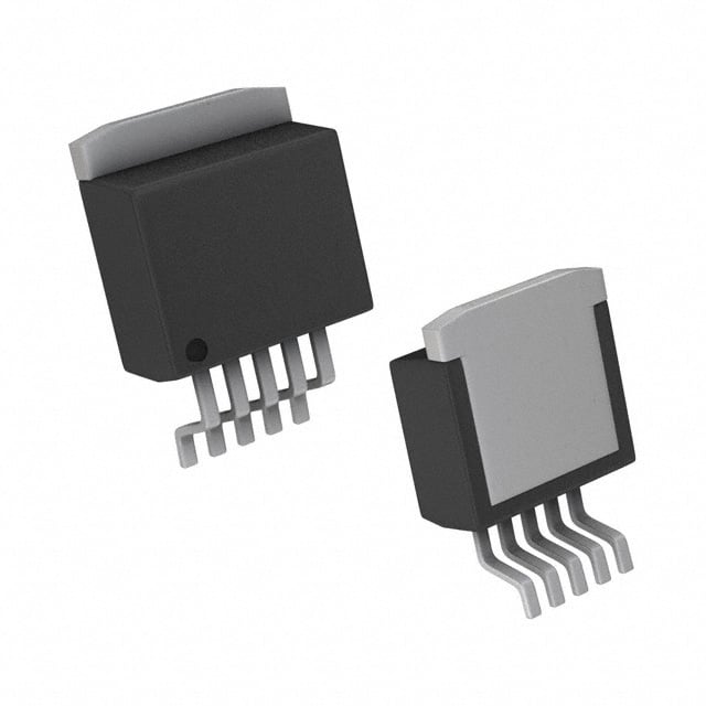
LME49610 SNAS435B–APRIL2008–REVISEDAPRIL2013 www.ti.com CONNECTION DIAGRAM TopView AV = 1 1 2 3 4 5 BW VEE VCC VIN VOUT Figure2. DDPAK/TO-263Package SeePackageNumberKTT0005B(1) (1) TheKTT0005Bpackageisanon-isolatedpackage.Thepackage’smetalbackandanyheatsinktowhichitismountedareconnected tothesamepotentialasthe–V pin. EE 2 SubmitDocumentationFeedback Copyright©2008–2013,TexasInstrumentsIncorporated ProductFolderLinks:LME49610
LME49610 www.ti.com SNAS435B–APRIL2008–REVISEDAPRIL2013 Thesedeviceshavelimitedbuilt-inESDprotection.Theleadsshouldbeshortedtogetherorthedeviceplacedinconductivefoam duringstorageorhandlingtopreventelectrostaticdamagetotheMOSgates. ABSOLUTE MAXIMUM RATINGS (1)(2)(3) SupplyVoltage 46V ESDRating (4) 2000V ESDRating (5) 200V StorageTemperature −40°Cto+150°C JunctionTemperature 150°C ThermalResistance θ 4°C/W JC θ 65°C/W JA θ (6) 20°C/W JA SolderingInformation:DDPAK/TO–263Package(10seconds) 260°C (1) “AbsoluteMaximumRatings”indicatelimitsbeyondwhichdamagetothedevicemayoccur,includinginoperabilityanddegradationof devicereliabilityand/orperformance.Functionaloperationofthedeviceand/ornon-degradationattheAbsoluteMaximumRatingsor otherconditionsbeyondthoseindicatedintheRecommendedOperatingConditionsisnotimplied.TheRecommendedOperating Conditionsindicateconditionsatwhichthedeviceisfunctionalandthedeviceshouldnotbeoperatedbeyondsuchconditions.All voltagesaremeasuredwithrespecttothegroundpin,unlessotherwisespecified (2) TheElectricalCharacteristicstableslistspecificationsunderthelistedRecommendedOperatingConditionsexceptasotherwise modifiedorspecifiedbytheElectricalCharacteristicsConditionsand/orNotes.Typicalspecificationsareestimationsonlyandarenot ensured. (3) IfMilitary/Aerospacespecifieddevicesarerequired,pleasecontacttheTexasInstrumentsSalesOffice/Distributorsforavailabilityand specifications. (4) Humanbodymodel,applicablestd.JESD22-A114C. (5) Machinemodel,applicablestd.JESD22-A115-A. (6) ThemaximumpowerdissipationmustbederatedatelevatedtemperaturesandisdictatedbyT ,θ ,andtheambienttemperature, JMAX JA T .ThemaximumallowablepowerdissipationisP =(T -T )/θ orthenumbergiveninAbsoluteMaximumRatings, A DMAX JMAX A JA whicheverislower.FortheLME49610,typicalapplicationshowninFigure27with|V |=V =15V,R =32Ω,thetotalpower EE CC L dissipationis1.9W.θ =20°C/WfortheDDPAK/TO-263packagemountedto16in2(103.2cm2)1oz.coppersurfaceheatsinkarea. JA OPERATING RATINGS (1)(2) TemperatureRange T ≤T ≤T −40°C≤T ≤85°C MIN A MAX A SupplyVoltage ±2.25Vto±22V (1) “AbsoluteMaximumRatings”indicatelimitsbeyondwhichdamagetothedevicemayoccur,includinginoperabilityanddegradationof devicereliabilityand/orperformance.Functionaloperationofthedeviceand/ornon-degradationattheAbsoluteMaximumRatingsor otherconditionsbeyondthoseindicatedintheRecommendedOperatingConditionsisnotimplied.TheRecommendedOperating Conditionsindicateconditionsatwhichthedeviceisfunctionalandthedeviceshouldnotbeoperatedbeyondsuchconditions.All voltagesaremeasuredwithrespecttothegroundpin,unlessotherwisespecified (2) TheElectricalCharacteristicstableslistspecificationsunderthelistedRecommendedOperatingConditionsexceptasotherwise modifiedorspecifiedbytheElectricalCharacteristicsConditionsand/orNotes.Typicalspecificationsareestimationsonlyandarenot ensured. Copyright©2008–2013,TexasInstrumentsIncorporated SubmitDocumentationFeedback 3 ProductFolderLinks:LME49610
LME49610 SNAS435B–APRIL2008–REVISEDAPRIL2013 www.ti.com ELECTRICAL CHARACTERISTICS ThefollowingspecificationsapplyforV =±22V,f =1kHz,R =1kΩ,unlessotherwisespecified.Typicalsandlimitsapply S IN L forT =25°C. A LME49610 Units Parameter TestConditions Typ (1) Limit (2) (Limits) I =0 OUT I TotalQuiescentCurrent BWpin:Noconnect 13 15 mA(max) Q BWpin:ConnectedtoV pin 19 23 mA(max) EE A =1,V =3V , V OUT RMS R =32Ω,BW=80kHz, L THD+N TotalHarmonicDistortion+Noise (3) closedloop(seeFigure27.) f=1kHz 0.000035 % f=20kHz 0.0005 % 30≤BW≤180MHz SR SlewRate 2000 V/μs V =20V ,R =100Ω OUT P-P L A =–3dB V BWpin:NoConnect R =100Ω 110 MHz L BW Bandwidth R =1kΩ 120 MHz L BWpin:ConnectedtoV pin EE R =100Ω 180 MHz L R =1kΩ 200 MHz L f=10kHz 3.0 8.5 nV/√Hz(max) BWpin:NoConnect VoltageNoiseDensity f=10kHz 2.7 6.5 nV/√Hz(max) BWpin:ConnectedtoV pin EE ΔV=10V,R =100Ω L 1%Accuracy t SettlingTime s BWpin:Noconnect 200 ns BWpin:ConnectedtoV pin 60 ns EE V =±10V OUT R =67Ω 0.93 0.90 V/V(min) A VoltageGain L V R =100Ω 0.95 0.92 V/V(min) L R =1kΩ 0.99 0.98 V/V(min) L Positive I =10mA V –1.2 V –1.4 V(min) OUT CC CC I =100mA V –1.5 V –1.8 V(min) OUT CC CC I =150mA V –1.7 V –2.1 V(min) OUT CC CC V VoltageOutput OUT Negative I =–10mA V +1.2 V +1.4 V(min) OUT EE EE I =–100mA V +1.6 V +1.9 V(min) OUT EE EE I =–150mA V +2.2 V +2.5 V(min) OUT EE EE I OutputCurrent ±250 mA OUT BWpin:NoConnect ±750 mA I ShortCircuitOutputCurrent OUT-SC BWpin:ConnectedtoV pin ±750 ±785 mA(max) EE V =0V IN I InputBiasCurrent BWpin:NoConnect ±1.0 ±2.5 μA(max) B BWpin:ConnectedtoV pin ±3.0 ±5.0 μA(max) EE R =100Ω L Z InputImpedance BWpin:NoConnect 7.5 MΩ IN BWpin:ConnectedtoV pin 5.5 MΩ EE V OffsetVoltage ±17 ±60 mV(max) OS V /°C OffsetVoltagevsTemperature 40°C≤T ≤+125°C ±100 μV/°C OS A PowerSupplyVoltageOperating ±2.25 V V SUPPLY Range ±22 V (1) TypicalvaluesrepresentmostlikelyparametricnormsatT =+25ºC,andattheRecommendedOperationConditionsatthetimeof A productcharacterizationandarenotensured. (2) Datasheetmin/maxspecificationlimitsarespecifiedbytestorstatisticalanalysis. (3) ThisisthedistortionoftheLME49610operatinginaclosedloopconfigurationwithanLME49710.Whenoperatinginanoperational amplifier'sfeedbackloop,theamplifier'sopenloopgaindominates,linearizingthesystemanddeterminingtheoverallsystemdistortion. 4 SubmitDocumentationFeedback Copyright©2008–2013,TexasInstrumentsIncorporated ProductFolderLinks:LME49610
LME49610 www.ti.com SNAS435B–APRIL2008–REVISEDAPRIL2013 TYPICAL PERFORMANCE CHARACTERISTICS GainvsFrequency PhasevsFrequency vsQuiescentCurrent vsQuiescentCurrent V =±22V V =±22V S S 20 0 IQ = 18.6 mA IQ = 18.6 mA 15 -10 IQ = 15.4 mA AIN (dB) 10 HASE (°) -20 G 5 P -30 IQ = 12.3 mA IQ = 15.4 mA 0 -40 IQ = 12.3 mA -5 -50 6 7 8 9 6 7 8 9 10 10 10 10 10 10 10 10 FREQUENCY (Hz) FREQUENCY (Hz) Figure3. Figure4. GainvsFrequency PhasevsFrequency vsPowerSupplyVoltage vsSupplyVoltage WideBWMode(BWpin=V ) WideBWMode(BWpin=V ) EE EE 20 0 VS = ±12V 15 VS = ±22V -10 VS = ±18V VS = ±12V AIN (dB) 10 VS = ±5V HASE (°) -20 VS = ±2.5V VS = ±22V G 5 P -30 VS = ±2.5V VS = ±5V 0 -40 VS = ±18V -5 -50 6 7 8 9 6 7 8 9 10 10 10 10 10 10 10 10 FREQUENCY (Hz) FREQUENCY (Hz) Figure5. Figure6. GainvsFrequency PhasevsFrequency vsPowerSupplyVoltage vsPowerSupplyVoltage LowI Mode(BWpin=Float) LowI Mode(BWpin=Float) Q Q 20 0 15 -10 AIN (dB) 10 VS V=S ± =1 2±V5V VS = ±22V HASE (°) -20 VS = ±15V VS = ±22V G 5 P -30 VS = ±2.5V VS = ±5V VS = ±18V 0 -40 VS = ±18V VS = ±2.5V -5 -50 6 7 8 9 6 7 8 9 10 10 10 10 10 10 10 10 FREQUENCY (Hz) FREQUENCY (Hz) Figure7. Figure8. Copyright©2008–2013,TexasInstrumentsIncorporated SubmitDocumentationFeedback 5 ProductFolderLinks:LME49610
LME49610 SNAS435B–APRIL2008–REVISEDAPRIL2013 www.ti.com TYPICAL PERFORMANCE CHARACTERISTICS (continued) GainvsFrequency PhasevsFrequency vsR vsR LOAD LOAD WideBWMode(BWpin=V ),V =±22V WideBWMode(BWpin=V ),V =±22V EE S EE S 20 0 R RLL = = 1 1 k0:0: R RL L= =1 1k0:0: 15 -10 AIN (dB) 10 HASE (°) -20 G 5 P -30 0 -40 RL = 50: RL = 50: -5 -50 6 7 8 9 6 7 8 9 10 10 10 10 10 10 10 10 FREQUENCY (Hz) FREQUENCY (Hz) Figure9. Figure10. GainvsFrequency PhasevsFrequency vsR vsR LOAD LOAD LowI Mode(BWpin=Float),V =±22V LowI Mode(BWpin=Float),V =±22V Q S Q S 20 0 RL = 1 k: RL = 100: RL = 100: RL = 1 k: 15 -10 AIN (dB) 10 HASE (°) -20 G 5 P -30 0 -40 RL = 50: RL = 50: -5 -50 6 7 8 9 6 7 8 9 10 10 10 10 10 10 10 10 FREQUENCY (Hz) FREQUENCY (Hz) Figure11. Figure12. GainvsFrequency PhasevsFrequency vsQuiescentCurrent vsQuiescentCurrent V =±15V V =±15V S S 0 20 IQ = 10.3 -10 15 IQ = 13.3 )B 10 E (°) -20 d S ( NIA PHA -30 G 5 IQ = 7.4 IQ = 13.3 mA -40 IQ = 10.3 mA 0 IQ=7.4 mA -50 -5 1M 10M 100M 1G 1M 10M 100M 1G FREQUENCY (Hz) FREQUENCY (Hz) Figure13. Figure14. 6 SubmitDocumentationFeedback Copyright©2008–2013,TexasInstrumentsIncorporated ProductFolderLinks:LME49610
LME49610 www.ti.com SNAS435B–APRIL2008–REVISEDAPRIL2013 TYPICAL PERFORMANCE CHARACTERISTICS (continued) GainvsFrequency PhasevsFrequency vsR vsR LOAD LOAD WideBWMode(BWpin=V ),V =±15V WideBWMode(BWpin=V ),V =±15V EE S EE S 0 20 15 RL = 1 k: -10 )B 10 E (°) -20 d S ( NIA RL = 100: PHA -30 G 5 -40 RL = 1 k: 0 RL = 100: RL = 50: RL = 50: -50 -5 1M 10M 100M 1G 1M 10M 100M 1G FREQUENCY (Hz) FREQUENCY (Hz) Figure15. Figure16. GainvsFrequency PhasevsFrequency vsR vsR LOAD LOAD LowI Mode(BWpin=Float),V =±15V LowI Mode(BWpin=Float),V =±15V Q S Q S 20 0 18 16 -10 14 12 GAIN (dB) 1086 RRLL == 11 0k0:: PHASE (°) --3200 4 RL = 50: RL = 1 k: 2 RL = 100: 0 -40 RL = 50: -2 -4 -50 1M 10M 100M 1G 1M 10M 100M 1G FREQUENCY (Hz) FREQUENCY (Hz) Figure17. Figure18. +PSRRvsFrequency +PSRRvsFrequency V =+15Vand±22V,WideBWMode V =±15Vand±22V,LowI Mode S S Q (BWpin=V ) (BWpin=Float) EE 80 80 70 70 60 60 B) 50 B) 50 R (d 40 R (d 40 R R S S P 30 P 30 20 20 10 10 0 0 20 200 2k 20k 200k 20 200 2k 20k 200k FREQUENCY (Hz) FREQUENCY (Hz) Figure19. Figure20. Copyright©2008–2013,TexasInstrumentsIncorporated SubmitDocumentationFeedback 7 ProductFolderLinks:LME49610
LME49610 SNAS435B–APRIL2008–REVISEDAPRIL2013 www.ti.com TYPICAL PERFORMANCE CHARACTERISTICS (continued) −PSRRvsFrequency −PSRRvsFrequency V =±15Vand±22V,WideBWMode V =±15Vand±22V,LowI Mode S S Q (BWpin=V ) (BWpin=Float) EE 80 80 70 70 60 60 B) 50 B) 50 R (d 40 R (d 40 R R S S P 30 P 30 20 20 10 10 0 0 20 200 2k 20k 200k 20 200 2k 20k 200k FREQUENCY (Hz) FREQUENCY (Hz) Figure21. Figure22. QuiescentCurrentvs BandwidthControlResistance THD+NvsOutputVoltage V =±15V(Bottom)&V =±22V(Top) V =±15V,R =32Ω,f=1kHz S S S L )Am 20 0.01 ( T N E 18 R R UC 16 0.001 YL %) PP 14 N ( U + S D REW 12 TH 0.0001 OP 10 T N EC 8 S E 0.00001 IU 6 0.000010.0001 0.001 0.01 0.1 1 10 Q 10 100 1000 10000 100000 RESISTANCE (:) OUTPUT POWER (W) Figure23. Figure24. WideBWNoiseCurve LowI NoiseCurve Q (BWpin=V ) (BWpin=Float) EE )z )z H 100 H 100 tr/V tr/V n n ( E ( E G G A A T T L L O O V V E E S S IO 10 IO 10 N N T T U U P P N N I T I T N N E E L L A A V V IU 1 IU 1 Q 1 10 100 1k 10k 100k Q 1 10 100 1k 10k 100k E E FREQUENCY (Hz) FREQUENCY (Hz) Figure25. Figure26. 8 SubmitDocumentationFeedback Copyright©2008–2013,TexasInstrumentsIncorporated ProductFolderLinks:LME49610
LME49610 www.ti.com SNAS435B–APRIL2008–REVISEDAPRIL2013 TYPICAL APPLICATION DIAGRAM RFB + V 0.1PF 10PF RIN + - VCC VCC 1 LME49860 IN LME49610 OUT 2 + VEE 0.1PF VEE 10PF RL + BW - V Figure27. HighPerformance,HighFidelityLME49610AudioBufferApplication APPLICATION INFORMATION HIGH PERFORMANCE, HIGH FIDELITY HEADPHONE AMPLIFIER The LME49610 is the ideal solution for high output, high performance high fidelity headphone amplifiers. When placed in the feedback loop of the LME49710, LME49720 or LME49740 High Performance, High Fidelity audio operational amplifier, the LME49610 is able to drive 32Ω headphones to a dissipation of greater than 500mW at 0.00003%THD+Nwhileoperatingon±15Vpowersupplyvoltages.Thecircuitschematicforatypicalheadphone amplifierisshowninFigure28. Operation The following describes the circuit operation for the headphone amplifier’s Left Channel. The Right Channel operatesidentically. The audio input signal is applied to the input jack (HP31 or J1/J2) and dc-coupled to the volume control, VR1. The output signal from VR1’s wiper is applied to the non-inverting input of U2-A, an LME49720 High Performance, High Fidelity audio operational amplifier. U2-A’s signal gain is set by resistors R2 and R4. To allow for a DC-coupled signal path and to ensure minimal output DC voltage regardless of the closed-loop gain, the other half of the U2 is configured as a DC servo. By constantly monitoring U2-A’s output, the servo creates a voltage that compensates for any DC voltage that may be present at the output. A correction voltage is generated and applied to the feedback node at U2-A, pin 2. The servo ensures that the gain at DC is unity. Based on the values shown in Figure 28, the RC combination formed by R11 and C7 sets the servo’s high-pass cutoffat0.16Hz.Thisisovertwodecadesbelow20Hz,minimizingbothamplitudeandphaseperturbationsinthe audiofrequencyband’slowestfrequencies. Copyright©2008–2013,TexasInstrumentsIncorporated SubmitDocumentationFeedback 9 ProductFolderLinks:LME49610
LME49610 SNAS435B–APRIL2008–REVISEDAPRIL2013 www.ti.com V+ C19 V+ 0.1 PF C1 C24 3 8 1.0 PF 2 5 4.+7 PF VR1-A + + 10k U1-A 1 U3 4 2 - LME49860NA 1 BW LME49610 R1 4 C2 3 C23 2 1k R3 + V- 1.0 PF 1k 4.7 PF J1 1 JU1 C20 C5 0.1 PF HP31 R9 1.0 PF V- HP32 453 1M 6 - LME498670NA R15k JU15 453 12 R11M0 5 +U1-CB6 U8 V+ C21 JU14 12 J 2 0.1 PF 1.0 PF C10 J2 1 5 + JU17 V+ 2 4.7 PF C3 + 4 U4 VR1-B 3 +8 1.0 PF 1 BW LME49610 10k U2-A 1 3 C9 2 - LME49860NA + 4.7 PF R2 4 C4 C22 1k R4 V- 1.0 PF 1k V- 0.1 PF C7 R11 1.0 PF 1M 6 LME49860NA R6 - 1k 7 R12 U2-B 5 + 1M C8 U4 J 1.0 PF Figure28. LME49610DeliversHighOutputCurrentforthisHighPerformanceHeadphoneAmplifier AUDIO BUFFERS Audio buffers or unity-gain followers, have large current gain and a voltage gain of one. Audio buffers serve many applications that require high input impedance, low output impedance and high output current. They also offerconstantgainoveraverywidebandwidth. Buffers serve several useful functions, either in stand-alone applications or in tandem with operational amplifiers. In stand-alone applications, their high input impedance and low output impedance isolates a high impedance sourcefromalowimpedanceload. SUPPLY BYPASSING The LME49610 will place great demands on the power supply voltage source when operating in applications that require fast slewing and driving heavy loads. These conditions can create high amplitude transient currents. A power supply’s limited bandwidth can reduce the supply’s ability to supply the needed current demands during these high slew rate conditions. This inability to supply the current demand is further exacerbated by PCB trace or interconnecting wire inductance. The transient current flowing through the inductance can produce voltage transients. 10 SubmitDocumentationFeedback Copyright©2008–2013,TexasInstrumentsIncorporated ProductFolderLinks:LME49610
LME49610 www.ti.com SNAS435B–APRIL2008–REVISEDAPRIL2013 Forexample,theLME49610’soutputvoltagecanslewatatypical2000V/μs.Whendrivinga100Ω load,thedi/dt current demand is 20 A/μs. This current flowing through an inductance of 50nH (approximately 1.5” of 22 gage wire) will produce a 1V transient. In these and similar situations, place the parallel combination of a solid 5μF to 10μFtantalumcapacitorandaceramic0.1μFcapacitorascloseaspossibletothedevicesupplypins. Ceramic capacitor have very lower ESR (typically less than 10mΩ) and low ESL when compared to the same valued tantalum capacitor. The ceramic capacitors, therefore, have superior AC performance for bypassing high frequencynoise. In less demanding applications that have lighter loads or lower slew rates, the supply bypassing is not as critical. Capacitorvaluesintherangeof0.01μFto0.1μFareadequate. SIMPLIFIED LME49610 CIRCUIT DIAGRAM The LME49610’s simplified circuit diagram is shown in Figure 29. The diagram shows the LME49610’s complementaryemitterfollowerdesign,biascircuitandbandwidthadjustmentnode. VCC Thermal Shutdown D1 - D7 Q5 Q3 Q1 IN Q2 OUT 200: Q4 Q6 BW D8 - D14 VEE Figure29. SimplifiedCircuitDiagram Figure 30 shows the LME49610 connected as an open-loop buffer. The source impedance and optional input resistor, R , can alter the frequency response. As previously stated, the power supplies should be bypassed with S capacitors connected close to the LME49610’s power supply pins. Capacitor values as low as 0.01μF to 0.1μF will ensure stable operation in lightly loaded applications, but high output current and fast output slewing can demand large current transients from the power supplies. Place a recommended parallel combination of a solid tantalum capacitor in the 5μF to 10μF range and a ceramic 0.1μF capacitor as close as possible to the device supplypins. Copyright©2008–2013,TexasInstrumentsIncorporated SubmitDocumentationFeedback 11 ProductFolderLinks:LME49610
LME49610 SNAS435B–APRIL2008–REVISEDAPRIL2013 www.ti.com V+ 10 PF + VCC IN OUT LME49610 RS VEE BW 10 PF+ RL V- Figure30. BufferConnections OUTPUT CURRENT The LME49610 can continuously source or sink 250mA. Internal circuitry limits the short circuit output current to approximately ±450mA. For many applications that fully utilize the LME49610’s current source and sink capabilities,thermaldissipationmaybethefactorthatlimitsthecontinuousoutputcurrent. The maximum output voltage swing magnitude varies with junction temperature and output current. Using sufficient PCB copper area as a heatsink when the metal tab of the LME49610’s surface mount DDPAK/TO-263 package is soldered directly to the circuit board reduces thermal impedance. This in turn reduces junction temperature.ThePCBcopperareashouldbeintherangeof2in2to6in2. THERMAL PROTECTION LME49610powerdissipatedwillcausethebuffer’sjunctiontemperaturetorise.Athermalprotectioncircuitinthe LME49610 will disable the output when the junction temperature exceeds 150°C. When the thermal protection is activated, the output stage is disabled, allowing the device to cool. The output circuitry is enabled when the junctiontemperaturedropsbelow150°C. The DSDPAK/TO-263 package has excellent thermal characteristics. To minimize thermal impedance, its exposed die attach paddle should be soldered to a circuit board copper area for good heat dissipation. Figure 31 shows typical thermal resistance from junction to ambient as a function of the copper area. The DDPAK/TO- 263’sexposeddieattachpaddleiselectricallyconnectedtotheV powersupplypin. EE LOAD IMPEDANCE The LME49610 is stable under any capacitive load when driven by a source that has an impedance of 50Ω or less. When driving capacitive loads, any overshoot that is present on the output signal can be reduced by shuntingtheloadcapacitancewitharesistor. OVERVOLTAGE PROTECTION If the input-to-output differential voltage exceeds the LME49610’s Absolute Maximum Rating of 3V, the internal diode clamps shown in Figure 1 conduct, diverting current around the compound emitter followers of Q1/Q5 (D1 – D7 for positive input), or around Q2/Q6 (D8 – D14 for negative inputs). Without this clamp, the input transistorsQ1/Q2andQ5/Q6willzeneranddamagethebuffer. Toensurethatthecurrentflowthroughthediodesisheldtoasavelevel,theinternal200Ω resistorinserieswith the input limits the current through these clamps. If the additional current that flows during this situation can damage the source that drives the LME49610’s input, add an external resistor in series with the input see Figure30. 12 SubmitDocumentationFeedback Copyright©2008–2013,TexasInstrumentsIncorporated ProductFolderLinks:LME49610
LME49610 www.ti.com SNAS435B–APRIL2008–REVISEDAPRIL2013 BANDWIDTH CONTROL PIN The LME49610’s –3dB bandwidth is approximately 110MHz in the low quiescent-current mode (13mA typical). SelectthismodebyleavingtheBWpinunconnected. Connect the BW pin to the V pin to extend the LME49610’s bandwidth to a nominal value of 180MHz. In this EE mode, the quiescent current increases to approximately 19mA. Bandwidths between these two limits are easily selectedbyconnectingaseriesresistorbetweentheBWpinandV . EE RegardlessoftheconnectiontotheLME49610’sBWpin,theratedoutputcurrentandslewrateremainconstant. With the power supply voltage held constant, the wide-bandwidth mode’s increased quiescent current causes a corresponding increase in quiescent power dissipation. For all values of the BW pin voltage, the quiescent power dissipationisequaltothetotalsupplyvoltagetimesthequiescentcurrent(I *(V +|V |)). Q CC EE BOOSTING OP AMP OUTPUT CURRENT When placed in the feedback loop, the LME49610 will increase an operational amplifier’s output current. The operationalamplifier’sopenloopgainwillcorrectanyLME49610errorswhileoperatinginsidethefeedbackloop. To ensure that the operational amplifier and buffer system are closed loop stable, the phase shift must be low. For a system gain of one, the LME49610 must contribute less than 20° at the operational amplifier’s unity-gain frequency. Various operating conditions may change or increase the total system phase shift. These phase shift changesmayaffecttheoperationalamplifier'sstability. Unity gain stability is preserved when the LME49610 is placed in the feedback loop of most general-purpose or precision op amps. When the LME46900 is driving high value capacitive loads, the BW pin should be connected to the V pin for wide bandwidth and stable operation. The wide bandwidth mode is also suggested for high EE speed or fast-settling operational amplifiers. This preserves their stability and the ability to faithfully amplify high frequency, fast-changing signals. Stability is ensured when pulsed signals exhibit no oscillations and ringing is minimized while driving the intended load and operating in the worst-case conditions that perturb the LME49610’sphaseresponse. HIGH FREQUENCY APPLICATIONS The LME49610’s wide bandwidth and very high slew rate make it ideal for a variety of high-frequency open-loop applicationssuchasanADCinputdriver,75Ω steppedvolumeattenuatordriver,andotherlowimpedanceloads. Circuit board layout and bypassing techniques affect high frequency, fast signal dynamic performance when the LME49610operatesopen-loop. A ground plane type circuit board layout is best for very high frequency performance results. Bypass the power supply pins (V and V ) with 0.1μF ceramic chip capacitors in parallel with solid tantalum 10μF capacitors CC EE placedascloseaspossibletotherespectivepins. Source resistance can affect high-frequency peaking and step response overshoot and ringing. Depending on the signal source, source impedance and layout, best nominal response may require an additional resistance of 25Ω to 200Ω in series with the input. Response with some loads (especially capacitive) can be improved with an outputseriesresistorintherangeof10Ω to150Ω. THERMAL MANAGEMENT HeatSinking For some applications, the LME49610 may require a heat sink. The use of a heat sink is dependent on the maximum LME49610 power dissipation and a given application’s maximum ambient temperature. In the DDPAK/TO-263 package, heat sinking the LME49610 is easily accomplished by soldering the package’s tab to a copper plane on the PCB. (Note: The tab on the LME49610’s DDPAK/TO-263 package is electrically connected toV .) EE Through the mechanisms of convection, heat conducts from the LME49610 in all directions. A large percentage moves to the surrounding air, some is absorbed by the circuit board material and some is absorbed by the copper traces connected to the package’s pins. From the PCB material and the copper, it then moves to the air. Naturalconvectiondependsontheamountofsurfaceareathatcontactstheair. Copyright©2008–2013,TexasInstrumentsIncorporated SubmitDocumentationFeedback 13 ProductFolderLinks:LME49610
LME49610 SNAS435B–APRIL2008–REVISEDAPRIL2013 www.ti.com If a heat conductive copper plane has perfect thermal conduction (heat spreading) through the plane’s total area, the temperature rise is inversely proportional to the total exposed area. PCB copper planes are, in that sense, an aid to convection. These planes, however, are not thick enough to ensure perfect heat conduction. Therefore, eventually a point of diminishing returns is reached where increasing copper area offers no additional heat conduction to the surrounding air. This is apparent in Figure 31. 2 oz copper boards will have decrease thermal resistanceprovidingabetterheatsinkcomparedto1oz.copper.Beyond1ozor2ozcopperplaneareas,external heatsinks are required. Ultimately, the 1oz copper area attains a nominal value of 20°C/W junction to ambient thermalresistance(θ )underzeroairflow. JA 70 )A 60 J T ( E C NA 50 D E P M I L 40 A M R E H 30 T 20 0 1 2 3 4 5 6 7 8 910111213141516 2 COPPER HEAT SINK AREA (in ) Figure31. ThermalResistance(Typ)for5LeadDDPAK/TO-263PackageMountedon1OunceofCopper A copper plane may be placed directly beneath the tab. Additionally, a matching plane can be placed on the opposite side. If a plane is placed on the side opposite of the LME49610, connect it to the plane to which the buffer’smetaltabissolderedwithamatrixofthermalviasperJEDECStandardJESD51-5. DeterminingCopperArea Findtherequiredcopperheatsinkareausingthefollowingguidelines: 1. DeterminethemaximumpowerdissipationoftheLME49610,P . D 2. Specify a maximum operating ambient temperature, T Note that the die temperature, T , will be higher A(MAX). J than T by an amount that is dependent on the thermal resistance from junction to ambient, θ . Therefore, A JA T mustbespecifiedsuchthatT doesnotexceedtheabsolutemaximumdietemperatureof150°C. A J 3. Specify a maximum allowable junction temperature, T , This is the LME49610’s die temperature when J(MAX) the buffer is drawing maximum current (quiescent and load). It is prudent to design for a maximum continuous junction temperature of 100°C to 130°C. Ensure, however, that the junction temperature never exceedsthe150°Cabsolutemaximumratingforthepart. 4. alculatethevalueofjunctiontoambientthermalresistance,θ . JA 5. θ as a function of copper area in square inches is shown in Figure 31. Choose a copper area that will JA ensure the specified T for the calculated θ . The maximum value of junction to ambient thermal J(MAX) JA resistance,θ ,isdefinedas: JA θ =(T -T )/P (°C/W) JA J(MAX) A(MAX) D(MAX) where • T =themaximumrecommendedjunctiontemperature J(MAX) • T =themaximumambienttemperatureintheLME49610’senvironment A(MAX) • P =themaximumrecommendedpowerdissipation D(MAX) • Theallowablethermalresistanceisdeterminedbythemaximumallowabletemperatureincrease: T =T -T (2) (2) RISE J(MAX) A(MAX) Thus, if ambient temperature extremes force T to exceed the design maximum, the part must be de-rated by RISE eitherdecreasingP toasafelevel,reducingθ further,or,ifavailable,usingalargercopperarea. D JA 14 SubmitDocumentationFeedback Copyright©2008–2013,TexasInstrumentsIncorporated ProductFolderLinks:LME49610
LME49610 www.ti.com SNAS435B–APRIL2008–REVISEDAPRIL2013 Procedure 1. First determine the maximum power dissipated by the LME49610, P . For the simple case of the buffer D(MAX) drivingaresistiveload,andassumingequalsupplies,P isgivenby: D(MAX) P =(I xV )+(V )2/(2π2R ) (Watts) (3) DMAX(AC) S S S L P =(I xV )+(V )2/R (Watts) DMAX(DC) S S S L where • V =|V |+V (V) S EE CC • I =quiescentsupplycurrent(A) S Equation3isforsinusoidaloutputvoltagesandEquation4isforDCoutputvoltages (4) 2. Determinethemaximumallowabledietemperaturerise, T =T -T °C (5) RISE(MAX) J(MAX) A(MAX) 3. Using the calculated value of T and P , find the required value of junction to ambient thermal RISE(MAX) D(MAX) resistancecombiningEquation1andEquation4toderiveEquation6: θ =T /P (°C/W) (6) JA RISE(MAX) D(MAX) 4. Finally,choosetheminimumvalueofcopperareafromFigure31basedonthevalueforθ . JA Example Assume the following conditions: V = |V | + V = 30V, R = 32Ω, I = 15mA, sinusoidal output voltage, T S EE CC L S J(MAX) =125°C,T =85°C A(MAX) ApplyingEquation3: P =(I xV )+(V )2/2π2R (7) DMAX S S S L =(15mA)(30V)+900V2/632Ω =1.87W ApplyingEquation4: T =125°C–85°C (8) RISE(MAX) =40°C ApplyingEquation6: θ =40°C/1.87W (9) JA =21.4°C/W Examining the Copper Area vs. θ plot (see Figure 31) indicates that a thermal resistance of 21.4°C/W is JA possible with a 8–10in2 plane of one layer of 1oz copper. Other solutions include using two layers of 1oz copper or the use of 2oz copper. Higher dissipation may require forced air flow. As a safety margin, an extra 15% heat sinkingcapabilityisrecommended. When amplifying AC signals, wave shapes and the nature of the load (reactive, non-reactive) also influence dissipation. Peak dissipation can be several times the average with reactive loads. It is particularly important to determinedissipationwhendrivinglargeloadcapacitance. The LME49610’s dissipation in DC circuit applications is easily computed using Equation 3. After the value of dissipationisdetermined,theheatsinkcopperareacalculationisthesameasforACsignals. SLEW RATE A buffer’s voltage slew rate is its output signal’s rate of change with respect to an input signal’s step changes. Forresistiveloads,slewrateislimitedbyinternalcircuitcapacitanceandoperatingcurrent(ingeneral,thehigher theoperatingcurrentforagiveninternalcapacitance,thehighertheslewrate). However, when driving capacitive loads, the slew rate may be limited by the available peak output current accordingtothefollowingexpression. dv/dt=I /C (10) PK L Copyright©2008–2013,TexasInstrumentsIncorporated SubmitDocumentationFeedback 15 ProductFolderLinks:LME49610
LME49610 SNAS435B–APRIL2008–REVISEDAPRIL2013 www.ti.com Output voltages with high slew rates will require large output load currents. For example if the part is required to slew at 1000V/μs with a load capacitance of 1nF, the current demanded from the LME49610 is 1A. Therefore, fast slew rate is incompatible with a capacitive load of this value. Also, if C is in parallel with the load, the peak L currentavailabletotheloaddecreasesasC increases. L + V Positive Regulator 300: 1 k: 6550: - +VREG + OUT 1 PF LM4040-5.0 LME49870 LME49610 Negative Regulator 300: 1 k: - LM4040-5.0 -VREG + OUT 1 PF - - 6550: V V LME49870 LME49610 - V Figure32. HighSpeedPositiveandNegativeRegulator 16 SubmitDocumentationFeedback Copyright©2008–2013,TexasInstrumentsIncorporated ProductFolderLinks:LME49610
LME49610 www.ti.com SNAS435B–APRIL2008–REVISEDAPRIL2013 REVISION HISTORY Rev Date Description 1.0 04/09/08 InitialWEBreleased. 1.01 10/28/09 TypicalandLimitchangesontheShortCircuitOutputcurrent. B 04/04/13 ChangedlayoutofNationalDataSheettoTIformat. Copyright©2008–2013,TexasInstrumentsIncorporated SubmitDocumentationFeedback 17 ProductFolderLinks:LME49610
PACKAGE OPTION ADDENDUM www.ti.com 11-Oct-2016 PACKAGING INFORMATION Orderable Device Status Package Type Package Pins Package Eco Plan Lead/Ball Finish MSL Peak Temp Op Temp (°C) Device Marking Samples (1) Drawing Qty (2) (6) (3) (4/5) LME49610TS/NOPB OBSOLETE DDPAK/ KTT 5 TBD Call TI Call TI -40 to 85 LME49610 TO-263 TS (1) The marketing status values are defined as follows: ACTIVE: Product device recommended for new designs. LIFEBUY: TI has announced that the device will be discontinued, and a lifetime-buy period is in effect. NRND: Not recommended for new designs. Device is in production to support existing customers, but TI does not recommend using this part in a new design. PREVIEW: Device has been announced but is not in production. Samples may or may not be available. OBSOLETE: TI has discontinued the production of the device. (2) Eco Plan - The planned eco-friendly classification: Pb-Free (RoHS), Pb-Free (RoHS Exempt), or Green (RoHS & no Sb/Br) - please check http://www.ti.com/productcontent for the latest availability information and additional product content details. TBD: The Pb-Free/Green conversion plan has not been defined. Pb-Free (RoHS): TI's terms "Lead-Free" or "Pb-Free" mean semiconductor products that are compatible with the current RoHS requirements for all 6 substances, including the requirement that lead not exceed 0.1% by weight in homogeneous materials. Where designed to be soldered at high temperatures, TI Pb-Free products are suitable for use in specified lead-free processes. Pb-Free (RoHS Exempt): This component has a RoHS exemption for either 1) lead-based flip-chip solder bumps used between the die and package, or 2) lead-based die adhesive used between the die and leadframe. The component is otherwise considered Pb-Free (RoHS compatible) as defined above. Green (RoHS & no Sb/Br): TI defines "Green" to mean Pb-Free (RoHS compatible), and free of Bromine (Br) and Antimony (Sb) based flame retardants (Br or Sb do not exceed 0.1% by weight in homogeneous material) (3) MSL, Peak Temp. - The Moisture Sensitivity Level rating according to the JEDEC industry standard classifications, and peak solder temperature. (4) There may be additional marking, which relates to the logo, the lot trace code information, or the environmental category on the device. (5) Multiple Device Markings will be inside parentheses. Only one Device Marking contained in parentheses and separated by a "~" will appear on a device. If a line is indented then it is a continuation of the previous line and the two combined represent the entire Device Marking for that device. (6) Lead/Ball Finish - Orderable Devices may have multiple material finish options. Finish options are separated by a vertical ruled line. Lead/Ball Finish values may wrap to two lines if the finish value exceeds the maximum column width. Important Information and Disclaimer:The information provided on this page represents TI's knowledge and belief as of the date that it is provided. TI bases its knowledge and belief on information provided by third parties, and makes no representation or warranty as to the accuracy of such information. Efforts are underway to better integrate information from third parties. TI has taken and continues to take reasonable steps to provide representative and accurate information but may not have conducted destructive testing or chemical analysis on incoming materials and chemicals. TI and TI suppliers consider certain information to be proprietary, and thus CAS numbers and other limited information may not be available for release. In no event shall TI's liability arising out of such information exceed the total purchase price of the TI part(s) at issue in this document sold by TI to Customer on an annual basis. Addendum-Page 1
PACKAGE OPTION ADDENDUM www.ti.com 11-Oct-2016 Addendum-Page 2
None
IMPORTANTNOTICE TexasInstrumentsIncorporatedanditssubsidiaries(TI)reservetherighttomakecorrections,enhancements,improvementsandother changestoitssemiconductorproductsandservicesperJESD46,latestissue,andtodiscontinueanyproductorserviceperJESD48,latest issue.Buyersshouldobtainthelatestrelevantinformationbeforeplacingordersandshouldverifythatsuchinformationiscurrentand complete.Allsemiconductorproducts(alsoreferredtohereinas“components”)aresoldsubjecttoTI’stermsandconditionsofsale suppliedatthetimeoforderacknowledgment. TIwarrantsperformanceofitscomponentstothespecificationsapplicableatthetimeofsale,inaccordancewiththewarrantyinTI’sterms andconditionsofsaleofsemiconductorproducts.TestingandotherqualitycontroltechniquesareusedtotheextentTIdeemsnecessary tosupportthiswarranty.Exceptwheremandatedbyapplicablelaw,testingofallparametersofeachcomponentisnotnecessarily performed. TIassumesnoliabilityforapplicationsassistanceorthedesignofBuyers’products.Buyersareresponsiblefortheirproductsand applicationsusingTIcomponents.TominimizetherisksassociatedwithBuyers’productsandapplications,Buyersshouldprovide adequatedesignandoperatingsafeguards. TIdoesnotwarrantorrepresentthatanylicense,eitherexpressorimplied,isgrantedunderanypatentright,copyright,maskworkright,or otherintellectualpropertyrightrelatingtoanycombination,machine,orprocessinwhichTIcomponentsorservicesareused.Information publishedbyTIregardingthird-partyproductsorservicesdoesnotconstitutealicensetousesuchproductsorservicesorawarrantyor endorsementthereof.Useofsuchinformationmayrequirealicensefromathirdpartyunderthepatentsorotherintellectualpropertyofthe thirdparty,oralicensefromTIunderthepatentsorotherintellectualpropertyofTI. ReproductionofsignificantportionsofTIinformationinTIdatabooksordatasheetsispermissibleonlyifreproductioniswithoutalteration andisaccompaniedbyallassociatedwarranties,conditions,limitations,andnotices.TIisnotresponsibleorliableforsuchaltered documentation.Informationofthirdpartiesmaybesubjecttoadditionalrestrictions. ResaleofTIcomponentsorserviceswithstatementsdifferentfromorbeyondtheparametersstatedbyTIforthatcomponentorservice voidsallexpressandanyimpliedwarrantiesfortheassociatedTIcomponentorserviceandisanunfairanddeceptivebusinesspractice. TIisnotresponsibleorliableforanysuchstatements. Buyeracknowledgesandagreesthatitissolelyresponsibleforcompliancewithalllegal,regulatoryandsafety-relatedrequirements concerningitsproducts,andanyuseofTIcomponentsinitsapplications,notwithstandinganyapplications-relatedinformationorsupport thatmaybeprovidedbyTI.Buyerrepresentsandagreesthatithasallthenecessaryexpertisetocreateandimplementsafeguardswhich anticipatedangerousconsequencesoffailures,monitorfailuresandtheirconsequences,lessenthelikelihoodoffailuresthatmightcause harmandtakeappropriateremedialactions.BuyerwillfullyindemnifyTIanditsrepresentativesagainstanydamagesarisingoutoftheuse ofanyTIcomponentsinsafety-criticalapplications. Insomecases,TIcomponentsmaybepromotedspecificallytofacilitatesafety-relatedapplications.Withsuchcomponents,TI’sgoalisto helpenablecustomerstodesignandcreatetheirownend-productsolutionsthatmeetapplicablefunctionalsafetystandardsand requirements.Nonetheless,suchcomponentsaresubjecttotheseterms. NoTIcomponentsareauthorizedforuseinFDAClassIII(orsimilarlife-criticalmedicalequipment)unlessauthorizedofficersoftheparties haveexecutedaspecialagreementspecificallygoverningsuchuse. OnlythoseTIcomponentswhichTIhasspecificallydesignatedasmilitarygradeor“enhancedplastic”aredesignedandintendedforusein military/aerospaceapplicationsorenvironments.BuyeracknowledgesandagreesthatanymilitaryoraerospaceuseofTIcomponents whichhavenotbeensodesignatedissolelyattheBuyer'srisk,andthatBuyerissolelyresponsibleforcompliancewithalllegaland regulatoryrequirementsinconnectionwithsuchuse. TIhasspecificallydesignatedcertaincomponentsasmeetingISO/TS16949requirements,mainlyforautomotiveuse.Inanycaseofuseof non-designatedproducts,TIwillnotberesponsibleforanyfailuretomeetISO/TS16949. Products Applications Audio www.ti.com/audio AutomotiveandTransportation www.ti.com/automotive Amplifiers amplifier.ti.com CommunicationsandTelecom www.ti.com/communications DataConverters dataconverter.ti.com ComputersandPeripherals www.ti.com/computers DLP®Products www.dlp.com ConsumerElectronics www.ti.com/consumer-apps DSP dsp.ti.com EnergyandLighting www.ti.com/energy ClocksandTimers www.ti.com/clocks Industrial www.ti.com/industrial Interface interface.ti.com Medical www.ti.com/medical Logic logic.ti.com Security www.ti.com/security PowerMgmt power.ti.com Space,AvionicsandDefense www.ti.com/space-avionics-defense Microcontrollers microcontroller.ti.com VideoandImaging www.ti.com/video RFID www.ti-rfid.com OMAPApplicationsProcessors www.ti.com/omap TIE2ECommunity e2e.ti.com WirelessConnectivity www.ti.com/wirelessconnectivity MailingAddress:TexasInstruments,PostOfficeBox655303,Dallas,Texas75265 Copyright©2016,TexasInstrumentsIncorporated