ICGOO在线商城 > 集成电路(IC) > 线性 - 音頻放大器 > MAX9725BETC+

 Datasheet下载
- 型号: MAX9725BETC+
- 制造商: Maxim
- 库位|库存: xxxx|xxxx
- 要求:
| 数量阶梯 | 香港交货 | 国内含税 |
| +xxxx | $xxxx | ¥xxxx |
查看当月历史价格
查看今年历史价格
MAX9725BETC+产品简介:
ICGOO电子元器件商城为您提供MAX9725BETC+由Maxim设计生产,在icgoo商城现货销售,并且可以通过原厂、代理商等渠道进行代购。 MAX9725BETC+价格参考。MaximMAX9725BETC+封装/规格:线性 - 音頻放大器, Amplifier IC Headphones, 2-Channel (Stereo) Class AB 12-TQFN (4x4)。您可以下载MAX9725BETC+参考资料、Datasheet数据手册功能说明书,资料中有MAX9725BETC+ 详细功能的应用电路图电压和使用方法及教程。
Maxim Integrated的MAX9725BETC+是一款D类音频功率放大器,常用于需要高效、小体积音频放大的应用场合。其应用场景主要包括:

1. 便携式音频设备:如便携音箱、蓝牙音箱等,得益于其高效率和小型封装,适合对功耗和空间有要求的设计。

2. 汽车音响系统:该器件具有良好的抗干扰性能和较高的电源效率,适用于车载音响系统中,提供清晰、强劲的音频输出。

3. 家用电器:如智能电视、迷你音响系统、家庭影院系统等,用于驱动扬声器,提供高质量音频体验。

4. 工业与专业音频设备:包括公共广播系统、会议系统、数字标牌等,适用于需要稳定音频输出的工业环境。

5. 电池供电设备:由于其高效率特性,减少了发热并延长了电池续航时间,适合使用电池供电的音频产品。

总之,MAX9725BETC+适用于对音质、效率和空间都有一定要求的中低功率音频放大应用。
| 参数 | 数值 |
| 产品目录 | 集成电路 (IC)半导体 |
| 描述 | IC AMP AUDIO .025W STER 12TQFN音频放大器 1V DirectDrive Headphone Amplifier |
| 产品分类 | |
| 品牌 | Maxim Integrated |
| 产品手册 | |
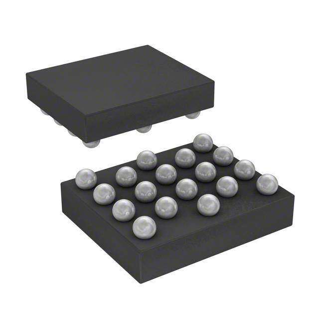
| 产品图片 |
|
| rohs | 符合RoHS无铅 / 符合限制有害物质指令(RoHS)规范要求 |
| 产品系列 | 音频 IC,音频放大器,Maxim Integrated MAX9725BETC+DirectDrive® |
| 数据手册 | |
| 产品型号 | MAX9725BETC+ |
| Pd-功率耗散 | 1.349 W |
| THD+噪声 | 0.006 % |
| 不同负载时的最大输出功率x通道数 | 25mW x 2 @ 16 欧姆 |
| 产品 | Audio Amplifiers |
| 产品培训模块 | http://www.digikey.cn/PTM/IndividualPTM.page?site=cn&lang=zhs&ptm=25703http://www.digikey.cn/PTM/IndividualPTM.page?site=cn&lang=zhs&ptm=25705 |
| 产品种类 | 音频放大器 |
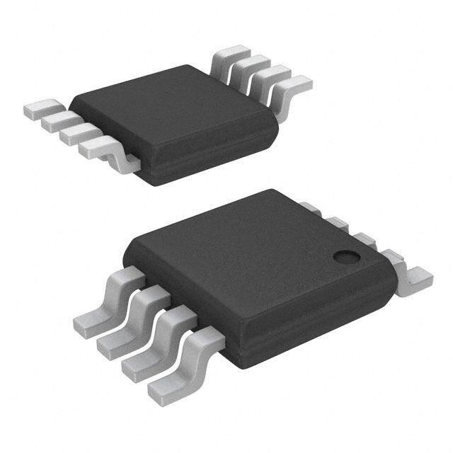
| 供应商器件封装 | 12-TQFN (4x4) |
| 包装 | 管件 |
| 商标 | Maxim Integrated |
| 安装类型 | 表面贴装 |
| 安装风格 | SMD/SMT |
| 封装 | Tube |
| 封装/外壳 | 12-WQFN 裸露焊盘 |
| 封装/箱体 | TQFN-EP-12 |
| 工作温度 | -40°C ~ 85°C (TA) |
| 工作电源电压 | 0.9 V to 1.8 V |
| 工厂包装数量 | 75 |
| 最大功率耗散 | 1.349 W |
| 最大工作温度 | + 85 C |
| 最小工作温度 | - 40 C |
| 标准包装 | 75 |
| 特性 | 消除爆音,短路保护,关机 |
| 电压-电源 | 900 mV ~ 1.8 V |
| 电源电流 | 2.1 mA |
| 类 | Class-AB |
| 类型 | 2-Channel Headphone |
| 系列 | MAX9725 |
| 输出功率 | 20 mW x 2 at 32 Ohms |
| 输出类型 | 耳机,2-通道(立体声) |
| 零件号别名 | MAX9725 |


- 商务部:美国ITC正式对集成电路等产品启动337调查
- 曝三星4nm工艺存在良率问题 高通将骁龙8 Gen1或转产台积电
- 太阳诱电将投资9.5亿元在常州建新厂生产MLCC 预计2023年完工
- 英特尔发布欧洲新工厂建设计划 深化IDM 2.0 战略
- 台积电先进制程称霸业界 有大客户加持明年业绩稳了
- 达到5530亿美元!SIA预计今年全球半导体销售额将创下新高
- 英特尔拟将自动驾驶子公司Mobileye上市 估值或超500亿美元
- 三星加码芯片和SET,合并消费电子和移动部门,撤换高东真等 CEO
- 三星电子宣布重大人事变动 还合并消费电子和移动部门
- 海关总署:前11个月进口集成电路产品价值2.52万亿元 增长14.8%


PDF Datasheet 数据手册内容提取
19-3465; Rev 4; 3/09 EVAALVUAAILTAIOBNL EKIT 1V, Low-Power, DirectDrive, Stereo Headphone Amplifier with Shutdown General Description Features M The MAX9725A–MAX9725D fixed-gain, stereo head- ♦ Low Quiescent Current A 2.1mA (MAX9725A–MAX9725D) phone amplifiers are ideal for portable equipment where 2.3mA (MAX9725E) X board space is at a premium. The MAX9725E offers the ♦ Single-Cell, 0.9V to 1.8V Single-Supply Operation flexibility to adjust the gain with external input and feed- 9 back resistors. The MAX9725A–MAX9725E use a unique ♦ Fixed Gain Eliminates External Feedback Network 7 MAX9725A: -2V/V DirectDrive architecture to produce a ground-referenced MAX9725B: -1.5V/V 2 output from a single supply, eliminating the need for large MAX9725C: -1V/V DC-blocking capacitors, saving cost, board space, and MAX9725D: -4V/V 5 component height. Fixed gains of -2V/V (MAX9725A), ♦ Adjustable Gain with External Input and Feedback -1.5V/V (MAX9725B), -1V/V (MAX9725C), and -4V/V Resistors (MAX9725D) further reduce external component count. MAX9725E: Minimum Stable Gain of -1V/V The adjustable gain of the MAX9725E DirectDrive head- ♦ Ground-Referenced Outputs Eliminate DC Bias phone amplifier allows for any gain down to -1V/V using ♦ No Degradation of Low-Frequency Response Due external resistors. to Output Capacitors The MAX9725 delivers up to 20mW per channel into a ♦ 20mW per Channel into 32Ω 32Ωload and achieves 0.006% THD+N. An 80dB at 1kHz ♦ Low 0.006% THD+N power-supply rejection ratio (PSRR) allows the MAX9725 ♦ High PSRR (80dB at 1kHz) to operate from noisy digital supplies without an additional ♦ Integrated Click-and-Pop Suppression linear regulator. The MAX9725 includes ±8kV ESD protec- ♦ Low-Power Shutdown Control tion on the headphone output. Comprehensive click-and- pop circuitry suppresses audible clicks and pops at ♦ Short-Circuit Protection startup and shutdown. A low-power shutdown mode ♦ ±8kV ESD-Protected Amplifier Outputs reduces supply current to 0.6µA (typ). ♦ Available in Space-Saving Packages 12-Bump UCSP (1.54mm x 2.02mm x 0.6mm) The MAX9725 operates from a single 0.9V to 1.8V supply, 12-Pin Thin QFN (4mm x 4mm x 0.8mm) allowing the device to be powered directly from a single AA or AAA battery. The MAX9725 consumes only Block Diagrams 2.1mA of supply current, provides short-circuit protection, and is specified over the extended -40°C to +85°C tem- perature range. The MAX9725 is available in a tiny (1.54mm x 2.02mm x 0.6mm) 12-bump chip-scale C3 SINGLE VDD 1.5V CELL package (UCSP™) and a 12-pin thin QFN package AA OR AAA (4mm x 4mm x 0.8mm). BATTERY Applications MAX9725A–MAX9725D MP3 Players Smart Phones DirectDrive OUTPUTS INL ELIMINATE DC-BLOCKING Cellular Phones Portable Audio Equipment CAPACITORS. PDAs OUTL Ordering Information C1P TO P GA I N INVERTING PVSS PAR T PIN-P AC KA G E MA R K (V /V) CHARGE PUMP C1N C2 MAX9725AEBC+ TG45 12 UC S P +A CK -2 VSS MA X9725AET C+ 12 TQFN-E P* +A AEW -2 MAX9725BEBC+ TG45 12 UC S P +A CL -1 .5 INR OUTR Ordering Information continued at end of data sheet. Note:All devices are specified over the -40°C to +85°C operating temperature range. SGND PGND +Denotes a lead(Pb)-free/RoHS-compliant package. T = Tape and reel. *EP = Exposed pad. Block Diagrams continued at end of data sheet. UCSP is a trademark of Maxim Integrated Products, Inc. Pin Configurations appear at end of data sheet. ________________________________________________________________Maxim Integrated Products 1 For pricing, delivery, and ordering information, please contact Maxim Direct at 1-888-629-4642, or visit Maxim’s website at www.maxim-ic.com.
1V, Low-Power, DirectDrive, Stereo Headphone Amplifier with Shutdown 5 ABSOLUTE MAXIMUM RATINGS 2 SGND to PGND.....................................................-0.3V to +0.3V SHDNto SGND or PGND.........................................-0.3V to +4V 7 VDDto SGND or PGND............................................-0.3V to +2V Output Short-Circuit Current......................................Continuous 9 VSSto PVSS...........................................................-0.3V to +0.3V Continuous Power Dissipation (TA= +70°C) X C1P to PGND..............................................-0.3V to (VDD+ 0.3V) 12-Bump UCSP (derate 6.5mW/°C above +70°C)....518.8mW C1N to PGND............................................(PVSS- 0.3V) to +0.3V 12-Pin Thin QFN (derate 16.9mW/°C above +70°C)..1349.1mW A VSS, PVSSto GND....................................................+0.3V to -2V Junction Temperature......................................................+150°C OUTR, OUTL, INR, INL to SGND Operating Temperature Range...........................-40°C to +85°C M (MAX9725A–MAX9725D)..............(VSS- 0.3V) to (VDD+ 0.3V) Storage Temperature Range.............................-65°C to +150°C OUTR, OUTL to SGND Bump Temperature (soldering) Reflow............................+230°C (MAX9725E)..................................(VSS- 0.3V) to (VDD+ 0.3V) Lead Temperature (soldering, 10s).................................+300°C INR, INL to SGND (MAX9725E)...................................-4V to +4V Stresses beyond those listed under “Absolute Maximum Ratings” may cause permanent damage to the device. These are stress ratings only, and functional operation of the device at these or any other conditions beyond those indicated in the operational sections of the specifications is not implied. Exposure to absolute maximum rating conditions for extended periods may affect device reliability. ELECTRICAL CHARACTERISTICS (MAX9725A–MAX9725D) (VDD= 1.5V, VPGND= VSGND= 0V, VSHDN= 1.5V, VSS= VPVSS, C1 = C2 = 1µF, CIN= 1µF, RL= ∞, TA= TMINto TMAX, unless other- wise noted. Typical values are at TA= +25°C.) (See the Functional Diagrams.) (Note 1) PARAMETER SYMBOL CONDITIONS MIN TYP MAX UNITS Supply Voltage Range VDD Guaranteed by PSRR test 0.9 1.8 V Quiescent Supply Current IDD Both channels active 2.1 3.3 mA TA = +25°C 0.6 10 Shutdown Current ISHDN VSHDN = 0V TA = -40°C to +85°C 30 µA Shutdown to Full Operation tON 180 µs VIH VDD = 0.9V to 1.8V 0.7 x VDD SHDN Thresholds V VIL VDD = 0.9V to 1.8V 0.3 x VDD SHDN Input Leakage Current ILEAK VDD = 0.9V to 1.8V (Note 2) ±1 µA CHARGE PUMP Oscillator Frequency fOSC 493 580 667 kHz AMPLIFIERS MAX9725A -2.04 -2.00 -1.96 MAX9725B -1.53 -1.5 -1.47 Voltage Gain AV V/V MAX9725C -1.02 -1.00 -0.98 MAX9725D -4.08 -4.00 -3.92 Gain Match ΔAV ±0.5 % Input AC-coupled, MAX9725A/MAX9725D ±0.3 ±1.05 Total Output Offset Voltage VOS RL = 32Ω to GND, MAX9725B ±0.45 ±1.58 mV TA = +25°C MAX9725C ±0.6 ±2.1 Input Resistance RIN 15 25 35 kΩ VDD = 0.9V to 1.8V, TA = +25°C 60 80 Power-Supply Rejection Ratio PSRR fIN = 1kHz 70 dB 100mVP-P ripple fIN = 20kHz 62 RL = 32Ω 10 20 VDD = 1.5V RL = 16Ω 25 Output Power (Note 3) POUT VDD = 1.0V, RL = 32Ω 7 mW VDD = 0.9V, RL = 32Ω 6 2 _______________________________________________________________________________________
1V, Low-Power, DirectDrive, Stereo Headphone Amplifier with Shutdown ELECTRICAL CHARACTERISTICS (MAX9725A–MAX9725D) (continued) M (VDD= 1.5V, VPGND= VSGND= 0V, VSHDN= 1.5V, VSS= VPVSS, C1 = C2 = 1µF, CIN= 1µF, RL= ∞, TA= TMINto TMAX, unless other- A wise noted. Typical values are at TA= +25°C.) (See the Functional Diagrams.) (Note 1) X PARAMETER SYMBOL CONDITIONS MIN TYP MAX UNITS 9 Total Harmonic Distortion Plus RL = 32Ω, POUT = 12mW, f = 1kHz 0.006 THD+N % 7 Noise RL = 16Ω, POUT = 15mW, f = 1kHz 0.015 2 BW = 22Hz to 22kHz 89 Signal-to-Noise Ratio SNR RL = 32Ω, POUT = 12mW dB 5 A-weighted filter 92 Slew Rate SR 0.2 V/µs Maximum Capacitive Load CL No sustained oscillations 150 pF Crosstalk XTALK fIN = 1.0kHz, RL = 32Ω, POUT = 5mW 100 dB RL = 32Ω, peak voltage, Into shutdown 72.8 Click-and-Pop Level KCP A-weighted, 32 samples per dBV second (Note 4) Out of shutdown 72.8 ESD Protection VESD Human Body Model (OUTR, OUTL) ±8 kV ELECTRICAL CHARACTERISTICS (MAX9725E) (VDD= 1.5V, VPGND= VSGND= 0V, VSHDN= 1.5V, VSS= VPVSS, C1 = C2 = 1µF, CIN= 1µF, RL= 32Ω, RF= 60kΩ, RIN= 10kΩ, TA= TMINto TMAX, unless otherwise noted. Typical values are at TA= +25°C.) (See the Functional Diagrams.) (Note 1) PARAMETER SYMBOL CONDITIONS MIN TYP MAX UNITS Supply Voltage Range VDD Guaranteed by PSRR test 0.9 1.8 V Quiescent Supply Current IDD Both channels active 2.3 3.7 mA TA = +25°C 0.6 1 Shutdown Current ISHDN VSHDN = 0V TA = -40°C to +85°C 10 µA Shutdown to Full Operation tON 180 µs VIH VDD = 0.9V to 1.8V 0.7 x VDD SHDN Thresholds V VIL VDD = 0.9V to 1.8V 0.3 x VDD SHDN Input Leakage Current ILEAK VDD = 0.9V to 1.8V (Note 2) ±1 µA CHARGE PUMP Oscillator Frequency fOSC 483 592 687 kHz AMPLIFIERS Voltage Gain AV (Note 5) -6.11 -6.07 -6.00 V/V Minimum Stable Gain ΔAV -1.0 V/V Input AC-coupled, RL = 32Ω to GND, Total Output Offset Voltage VOS TA = +25°C (Note 6) ±0.63 ±2.1 mV Input Resistance RIN 6.3 9.78 14 kΩ INR, INL Input Leakage ILK ±100 nA Current Maximum Input Parasitic CPAR 5 pF Capacitance VDD = 0.9V to 1.8V, TA = +25°C 52.9 67.8 Power-Supply Rejection Ratio PSRR 100mVP-P ripple fIN = 1kHz 70 dB (Note 5) fIN = 20kHz 62 _______________________________________________________________________________________ 3
1V, Low-Power, DirectDrive, Stereo Headphone Amplifier with Shutdown 5 ELECTRICAL CHARACTERISTICS (MAX9725E) (continued) 2 (VDD= 1.5V, VPGND= VSGND= 0V, VSHDN= 1.5V, VSS= VPVSS, C1 = C2 = 1µF, CIN= 1µF, RL= 32Ω, RF= 60kΩ, RIN= 10kΩ, TA= 7 TMINto TMAX, unless otherwise noted. Typical values are at TA= +25°C.) (See the Functional Diagrams.) (Note 1) 9 PARAMETER SYMBOL CONDITIONS MIN TYP MAX UNITS X RL = 32Ω 10 24 A VDD = 1.5V RL = 16Ω 25 M Output Power (Note 3) POUT VDD = 1.0V, RL = 32Ω 7 mW VDD = 0.9V, RL = 32Ω 6 Total Harmonic Distortion Plus RL = 32Ω, POUT = 12mW, f = 1kHz 0.006 THD+N % Noise (Note 5) RL = 16Ω, POUT = 15mW, f = 1kHz 0.015 BW = 22Hz to 22kHz 89 Signal-to-Noise Ratio SNR RL = 32Ω, POUT = 12mW dB A-weighted filter 92 Slew Rate SR 0.3 V/µs Maximum Capacitive Load CL No sustained oscillations 150 pF Crosstalk XTALK fIN = 1.0kHz, RL = 32Ω, POUT = 5mW 100 dB RL = 32Ω, peak voltage, Into shutdown 72.8 Click-and-Pop Level KCP A-weighted, 32 samples per dBV second (Note 4) Out of shutdown 72.8 ESD Protection VESD Human Body Model (OUTR, OUTL) ±8 kV RL = 32Ω -120 Attenuation in Shutdown ATT(SD) VSHDN = 0V RL = 10kΩ -75 dB Note 1: All specifications are 100% tested at TA= +25°C; temperature limits are guaranteed by design. Note 2: Input leakage current measurements limited by automated test equipment. Note 3: fIN= 1kHz, TA= +25°C, THD+N < 1%, both channels driven in-phase. Note 4: Testing performed with 32Ωresistive load connected to outputs. Mode transitions controlled by SHDN. KCPlevel calculated as 20 log [peak voltage under normal operation at rated power level / peak voltage during mode transition]. Inputs are AC- grounded. Note 5: Using existing resistors with 1% precision. Note 6: RIN= 10Ω, RF=10kΩ. Typical Operating Characteristics (VDD= 1.5V, VPGND= VSGND= 0V, VSHDN= 1.5V, VSS= VPVSS, C1 = C2 = 1µF, CIN= 1µF, THD+N measurement bandwidth = 22Hz to 22kHz, TA= +25°C, unless otherwise noted.) (See the Functional Diagrams.) TOTAL HARMONIC DISTORTION PLUS TOTAL HARMONIC DISTORTION PLUS TOTAL HARMONIC DISTORTION PLUS NOISE vs. FREQUENCY NOISE vs. FREQUENCY NOISE vs. FREQUENCY 1 VARDLV D== =1- 261VΩ.5/VV MAX9725 toc01 1 VRADLV D== =3- 221VΩ.5/VV MAX9725 toc02 1 VRADLV D== =1- 261VΩV/V MAX9725 toc03 0.1 0.1 0.1 POUT = 0.7mW %) POUT = 15mW %) %) N ( N ( POUT = 2mW N ( + + + D D D H H H T T T 0.01 0.01 0.01 POUT = 2mW POUT = 4mW POUT = 12mW 0.001 0.001 0.001 10 100 1k 10k 100k 10 100 1k 10k 100k 10 100 1k 10k 100k FREQUENCY (Hz) FREQUENCY (Hz) FREQUENCY (Hz) 4 _______________________________________________________________________________________
1V, Low-Power, DirectDrive, Stereo Headphone Amplifier with Shutdown Typical Operating Characteristics (continued) M (VDD= 1.5V, VPGND= VSGND= 0V, VSHDN= 1.5V, VSS= VPVSS, C1 = C2 = 1µF, CIN= 1µF, THD+N measurement bandwidth = 22Hz A to 22kHz, TA= +25°C, unless otherwise noted.) (See the Functional Diagrams.) X TOTAL HARMONIC DISTORTION PLUS TOTAL HARMONIC DISTORTION PLUS TOTAL HARMONIC DISTORTION PLUS 9 NOISE vs. FREQUENCY NOISE vs. OUTPUT POWER NOISE vs. OUTPUT POWER 1 VRADLV D== =3- 221VΩV/V MAX9725 toc04 11000 AVRDLV D== =1- 261VΩ.5/VV ffIINN == 210kHHzz MAX9725 toc05 11000 VRADLV D== =3- 221VΩ.5/VV ffIINN == 12k0HHzz MAX9725 toc06 725 0.1 THD+N (%) POUT = 0.7mW THD+N (%) 0.11 fIN = 10kHz THD+N (%) 0.11 fIN = 10kHz 0.01 0.01 0.01 POUT = 4mW 0.001 0.001 0.001 10 100 1k 10k 100k 0 10 20 30 40 0 10 20 30 40 FREQUENCY (Hz) OUTPUT POWER (mW) OUTPUT POWER (mW) TOTAL HARMONIC DISTORTION PLUS TOTAL HARMONIC DISTORTION PLUS POWER-SUPPLY REJECTION RATIO NOISE vs. OUTPUT POWER NOISE vs. OUTPUT POWER vs. FREQUENCY 11000 VARDLV D== =1- 261VΩV/V ffIINN == 210kHHzz MAX9725 toc07 10100 VRADLV D== =3- 221VΩV/V ffIINN == 12k0HHzz MAX9725 toc08 ---132000 VRDL D= =3 21Ω.5V MAX9725 toc09 -40 THD+N (%) 0.11 fIN = 10kHz THD+N (%) 0.11 fIN = 10kHz PSRR (dB) ---657000 -80 0.01 0.01 -90 -100 0.001 0.001 -110 0 5 10 15 0 5 10 15 10 100 1k 10k 100k OUTPUT POWER (mW) OUTPUT POWER (mW) FREQUENCY(Hz) POWER-SUPPLY REJECTION RATIO vs. FREQUENCY CROSSTALK vs. FREQUENCY OUTPUT POWER vs. SUPPLY VOLTAGE --21000 VRDL D= =3 21ΩV MAX9725 toc10 -200 VPRDOL DU=T =3 = 21 Ω5.5mVW MAX9725 toc11 7800 RBfINLO T==H 11 6kINHΩPzUTS MAX9725 toc12 60 DRIVEN IN-PHASE -30 -40 mW) PSRR (dB) ---546000 PSRR (dB) --6800 LEFT TO RIGHT UTPUT POWER ( 345000 THD+N = 10% -70 O 20 -80 -100 10 -90 RIGHT TO LEFT THD+N = 1% -100 -120 0 10 100 1k 10k 100k 10 100 1k 10k 100k 0.9 1.1 1.3 1.5 FREQUENCY (Hz) FREQUENCY (Hz) SUPPLY VOLTAGE (V) _______________________________________________________________________________________ 5
1V, Low-Power, DirectDrive, Stereo Headphone Amplifier with Shutdown 5 Typical Operating Characteristics (continued) 2 (VDD= 1.5V, VPGND= VSGND= 0V, VSHDN= 1.5V, VSS= VPVSS, C1 = C2 = 1µF, CIN= 1µF, THD+N measurement bandwidth = 22Hz 7 to 22kHz, TA= +25°C, unless otherwise noted.) (See the Functional Diagrams.) 9 OUTPUT POWER OUTPUT POWER OUTPUT POWER X vs. SUPPLY VOLTAGE vs. LOAD RESISTANCE vs. LOAD RESISTANCE MA 445050 fRBINLO T==H 31 2kINHΩPzUTS MAX9725 toc13 8700 VfBINDO DT= H =1 kI1NH.5PzVUTS MAX9725 toc14 8700 VfBINDO DT= H =1 kI1NHVPzUTS MAX9725 toc15 DRIVEN IN-PHASE 60 DRIVEN IN-PHASE 60 DRIVEN IN-PHASE mW) 35 W) THD+N = 10% W) WER ( 30 THD+N = 10% ER (m 50 ER (m 50 OUTPUT PO 122505 UTPUT POW 4300 THD+N = 1% UTPUT POW 4300 THD+N =T H1D0%+N = 1% O 20 O 20 10 5 THD+N = 1% 10 10 0 0 0 0.9 1.1 1.3 1.5 10 100 1k 10 100 1k SUPPLY VOLTAGE (V) LOAD RESISTANCE (Ω) LOAD RESISTANCE (Ω) POWER DISSIPATION POWER DISSIPATION GAIN FLATNESS vs. OUTPUT POWER vs. OUTPUT POWER vs. FREQUENCY mW) 678000 RL = 16Ω MAX9725 toc16 mW) 233505 MAX9725 toc17 -2101 MAX9725 toc18 R DISSIPATION ( 345000 R DISSIPATION ( 1250 RL = 16Ω PLITUDE (dB) ----2345 OWE OWE 10 AM -6 P 1200 RL = 32Ω VfPINDO DU= T =1 = k1 HP.5zOVUTL + POUTR P 5 RL = 32Ω VfPINDO DU= T =1 = k1 HPVzOUTL + POUTR --78 OUTPUTS IN-PHASE OUTPUTS IN-PHASE -9 0 0 -10 0 10 20 30 40 50 0 5 10 15 20 10 100 1k 10k 100k OUTPUT POWER (mW) OUTPUT POWER (mW) FREQUENCY(Hz) OUTPUT POWER vs. CHARGE-PUMP OUTPUT SPECTRUM SUPPLY CURRENT CAPACITANCE AND LOAD RESISTANCE vs. FREQUENCY vs. SUPPLY VOLTAGE W) 334050 C1 = C2 = 2.C21μ F= C2 = 1μF MAX9725 toc19 --42000 fRVVINLOD UD==T =31 = 2k1 HΩ-.56zV0dBV MAX9725 toc20 mA) 3445....5050 NO LOAD MAX9725 toc21 OUTPUT POWER (m 11220505 C1 = C2 = 0.68μF AMPLITUDE (dB)--11--86200000 SUPPLY CURRENT ( 1223....5050 VDD = 1.5V 1.0 5 C1 = C2 = 0.47μF fIN = 1kHz -140 0.5 THD+N = 1% 0 -160 0 10 20 30 40 50 0 5 10 15 20 0.9 1.0 1.1 1.2 1.3 1.4 1.5 LOAD RESISTANCE (Ω) FREQUENCY (kHz) SUPPLY VOLTAGE (V) 6 _______________________________________________________________________________________
1V, Low-Power, DirectDrive, Stereo Headphone Amplifier with Shutdown Typical Operating Characteristics (continued) M (VDD= 1.5V, VPGND= VSGND= 0V, VSHDN= 1.5V, VSS= VPVSS, C1 = C2 = 1µF, CIN= 1µF, THD+N measurement bandwidth = 22Hz A to 22kHz, TA= +25°C, unless otherwise noted.) (See the Functional Diagrams.) X SHUTDOWN CURRENT 9 vs. SUPPLY VOLTAGE EXITING SHUTDOWN POWER-UP/-DOWN WAVEFORM 7 00..67 MAX9725 toc22 MAX9725 toc23 MAX9725toc24 VDD 25 A) OUT_ 1V/div μT ( 0.5 1V/div N E RR 0.4 U N C SHDN W 0.3 500mV/div O D T HU 0.2 OUT_ S 10mV/div 0.1 0 0.9 1.1 1.3 1.5 200μs/div 200ms/div SUPPLY VOLTAGE (V) Pin Description PIN BUMP THIN NAME FUNCTION UCSP QFN 1 A1 C1N Flying Capacitor Negative Terminal. Connect a 1µF capacitor from C1P to C1N. Inverting Charge-Pump Output. Bypass with 1µF from PVSS to PGND. PVSS must be connected to 2 A2 PVSS VSS. Left-Amplifier Inverting Input. Connect input resistor RIN from input capacitor C1N to INL (MAX9725E 3 A3 INL only). Right-Amplifier Inverting Input. Connect input resistor RIN from input capacitor C1N to INR 4 A4 INR (MAX9725E only). 5 B4 VSS Amplifier Negative Power Supply. Must be connected to PVSS. Signal Ground. SGND must be connected to PGND. SGND is the ground reference for the input and 6 B3 SGND output signal. 7 C4 OUTR Right-Channel Output. Connect feedback resistor RFB between OUTR and INR (MAX9725E only). 8 C3 OUTL Left-Channel Output. Connect feedback resistor RFB between OUTL and INL (MAX9725E only). 9 C2 VDD Positive Power-Supply Input. Bypass with a 1µF capacitor to PGND. 10 C1 C1P Flying Capacitor Positive Terminal. Connect a 1µF capacitor from C1P to C1N. 11 B1 PGND Power Ground. Ground reference for the internal charge pump. PGND must be connected to SGND. Active-Low Shutdown. Connect to VDD for normal operation. Pull low to disable the amplifier and 12 B2 SHDN charge pump. EP — EP Exposed Paddle. Internally connected to VSS. Leave paddle unconnected or solder to VSS. _______________________________________________________________________________________ 7
1V, Low-Power, DirectDrive, Stereo Headphone Amplifier with Shutdown 5 Detailed Description Previous attempts to eliminate the output-coupling 2 capacitors involved biasing the headphone return The MAX9725 stereo headphone driver features Maxim’s (sleeve) to the DC-bias voltage of the headphone 7 DirectDrive architecture, eliminating the large output-cou- amplifiers. This method raises some issues: 9 pling capacitors required by conventional single-supply X headphone drivers. The MAX9725 consists of two 20mW • The sleeve is typically grounded to the chassis. class AB headphone drivers, shutdown control, inverting Using this biasing approach, the sleeve must be A charge pump, internal gain-setting resistors, and compre- isolated from system ground, complicating product M hensive click-and-pop suppression circuitry (see the design. Functional Diagrams). A negative power supply (PVSS) is • During an ESD strike, the driver’s ESD structures created by inverting the positive supply (VDD). Powering are the only path to system ground. The driver must the drivers from VDD and PVSS increases the dynamic be able to withstand the full ESD strike. range of the drivers to almost twice that of other 1V sin- • When using the headphone jack as a line out to gle-supply drivers. This increase in dynamic range allows other equipment, the bias voltage on the sleeve may for higher output power. conflict with the ground potential from other equip- The outputs of the MAX9725 are biased about GND ment, resulting in possible damage to the drivers. (Figure 1). The benefit of this GND bias is that the driver outputs do not have a DC component, thus large DC- blocking capacitors are unnecessary. Eliminating the DC-blocking capacitors on the output saves board space, system cost, and improves frequency response. VDD DirectDrive Conventional single-supply headphone drivers have their outputs biased about a nominal DC voltage (typically half VOUT VDD / 2 the supply) for maximum dynamic range. Large coupling GND capacitors are needed to block the DC bias from the headphones. Without these capacitors, a significant amount of DC current flows to the headphone, resulting in unnecessary power dissipation and possible damage to both headphone and headphone driver. CONVENTIONAL DRIVER-BIASING SCHEME Maxim’s DirectDrive architecture uses a charge pump to create an internal negative supply voltage. This allows the MAX9725 outputs to be biased about GND, increasing the dynamic range while operating from a VDD single supply. A conventional amplifier powered from 1.5V ideally provides 18mW to a 16Ω load. The MAX9725 provides 25mW to a 16Ω load. The DirectDrive architecture eliminates the need for two VOUT GND large (220µF, typ) DC-blocking capacitors on the out- put. The MAX9725 charge pump requires two small ceramic capacitors, conserving board space, reducing cost, and improving the frequency response of the -VDD headphone driver. See the Output Power vs. Charge- Pump Capacitance and Load Resistance graph in the DirectDrive BIASING SCHEME Typical Operating Characteristics for details of the possi- ble capacitor sizes. Figure 1. Traditional Driver Output Waveform vs. MAX9725 Output Waveform (Ideal Case) 8 _______________________________________________________________________________________
1V, Low-Power, DirectDrive, Stereo Headphone Amplifier with Shutdown M ADDITIONAL THD+N DUE LF ROLLOFF (16Ω LOAD) TO DC-BLOCKING CAPACITORS 0 A 10 -3 330μF X -5 220μF 9 1 -10 ON (dB) -15 100μF -130d0Bμ FC OISR 1N0E0RH FzOR %) 0.1 72 NUATI -20 33μF D+N ( TANTALUM 5 TTE TH 0.01 A -25 -30 0.001 ALUM/ELEC -35 0.0001 10 100 1k 10 100 1k 10k 100k FREQUENCY (Hz) FREQUENCY (Hz) Figure 2. Low-Frequency Attenuation for Common DC-Blocking Figure 3. Distortion Contributed By DC-Blocking Capacitors Capacitor Values Low-Frequency Response voltage coefficient appears as frequency-dependent Large DC-blocking capacitors limit the amplifier’s low- distortion. Figure 3 shows the THD+N introduced by frequency response and can distort the audio signal: two different capacitor dielectric types. Note that below 100Hz, THD+N increases rapidly. 1) The impedance of the headphone load and the DC- blocking capacitor forms a highpass filter with the The combination of low-frequency attenuation and fre- -3dB point set by: quency-dependent distortion compromises audio reproduction in portable audio equipment that empha- sizes low-frequency effects such as multimedia lap- 1 f-3dB= 2πR C tops, as well as MP3, CD, and DVD players. These L OUT low-frequency, capacitor-related deficiencies are elimi- nated by using DirectDrive technology. where RL is the impedance of the headphone and COUTis the value of the DC-blocking capacitor. The Charge Pump highpass filter is required by conventional single- The MAX9725 features a low-noise charge pump. The ended, single power-supply headphone drivers to 580kHz switching frequency is well beyond the audio block the midrail DC-bias component of the audio range, and does not interfere with the audio signals. signal from the headphones. The drawback to the The switch drivers feature a controlled switching speed filter is that it can attenuate low-frequency signals. that minimizes noise generated by turn-on and turn-off Larger values of COUT reduce this effect but result transients. The di/dt noise caused by the parasitic bond in physically larger, more expensive capacitors. wire and trace inductance is minimized by limiting the Figure 2 shows the relationship between the size of turn-on/off speed of the charge pump. Additional high- COUT and the resulting low-frequency attenuation. frequency noise attenuation can be achieved by Note that the -3dB point for a 16Ω headphone with increasing the size of C2 (see the Functional Diagrams). a 100µF blocking capacitor is 100Hz, well within the Extra noise attenuation is not typically required. normal audio band, resulting in low-frequency Shutdown attenuation of the reproduced signal. The MAX9725’s low-power shutdown mode reduces 2) The voltage coefficient of the DC-blocking capacitor supply current to 0.6µA. Driving SHDN low disables the contributes distortion to the reproduced audio signal amplifiers and charge pump. The driver’s output imped- as the capacitance value varies when the function of ance is typically 50kΩ (MAX9725A), 37.5kΩ the voltage across the capacitor changes. At low (MAX9725B), 25kΩ (MAX9725C), 100kΩ (MAX9725D), frequencies, the reactance of the capacitor domi- or RF(MAX9725E) when in shutdown mode. nates at frequencies below the -3dB point and the _______________________________________________________________________________________ 9
1V, Low-Power, DirectDrive, Stereo Headphone Amplifier with Shutdown 5 Applications Information 2 OUTPUT POWER vs. SUPPLY VOLTAGE WITH INPUTS IN- AND OUT-OF-PHASE Power Dissipation 7 50 Linear power amplifiers can dissipate a significant 9 45 fRINL == 116kHΩz amount of power under normal operating conditions. X 40 THD+N = 1% The maximum power dissipation for each package is MA WER (mW) 3305 INPUTS 180° OUT-OF-PHASE gCthiovene ftnoin lliuonow utihnseg P Aeoqbwuseoarlt uiDotenis :sMipaaxtiimonu mo r Rcaatnin gbse sceaclctiuolna teudnd beyr O 25 P T U 20 P T -T OUT 15 PDISSPKG(MAX) = J(MθAX) A 10 JA INPUTS IN-PHASE 5 where TJ(MAX) is +150°C, TA is the ambient tempera- 0 ture, and θJA is the reciprocal of the derating factor in 0.9 1.1 1.3 1.5 °C/W as specified in the Absolute Maximum Ratings SUPPLY VOLTAGE (V) section. For example, θJA for the thin QFN package is +59.3°C/W. Figure 4. Output Power vs. Supply Voltage with Inputs In-/Out- of-Phase The MAX9725 has two power dissipation sources, the charge pump and the two amplifiers. If the power dissi- pation exceeds the rated package dissipation, reduce Click-and-Pop Suppression VDD, increase load impedance, decrease the ambient In conventional single-supply audio drivers, the output- temperature, or add heatsinking to the device. Large coupling capacitor is a major contributor of audible output, supply, and ground traces decrease θJA, allow- clicks and pops. Upon startup, the driver charges the ing more heat to be transferred from the package to coupling capacitor to its bias voltage, typically half the surrounding air. supply. Likewise, on shutdown, the capacitor is dis- charged to GND. This results in a DC shift across the Output Power capacitor that appears as an audible transient at the The MAX9725’s output power increases when the left speaker. The MAX9725’s DirectDrive technology elimi- and right audio signals differ in magnitude and/or nates the need for output-coupling capacitors. phase. Figure 4 shows the two extreme cases for in- and out-of-phase input signals. The output power of a The MAX9725 also features extensive click-and-pop typical stereo application lies between the two extremes suppression that eliminates any audible transient shown in Figure 4. The MAX9725 is specified to output sources internal to the device. The Power-Up/-Down 20mW per channel when both inputs are in-phase. Waveform in the Typical Operating Characteristics shows minimal DC shift and no spurious transients at Powering Other Circuits from the output upon startup or shutdown. the Negative Supply The MAX9725 internally generates a negative supply In most applications, the output of the preamplifier dri- ving the MAX9725 has a DC bias of typically half the voltage (PVSS) to provide the ground-referenced output supply. At startup, the input-coupling capacitor is signal. Other devices can be powered from PVSS pro- vided the current drawn from the charge pump does charged to the preamplifier’s DC bias voltage through not exceed 1mA. Headphone driver output power and the internal input resistor (25kΩ for MAX9725A- THD+N will be adversely affected if more than 1mA is MAX9725D, minimum 10kΩ for MAX9725E) causing an audible click and pop. Delaying the rise of SHDN 4 or 5 drawn from PVSS. Using PVSSas an LCD bias is a typi- cal application for the negative supply. time constants, based on RIN x CIN, relative to the start- up of the preamplifier eliminates any click and pop PVSS is unregulated and proportional to VDD. Connect caused by the input filter (see the Functional Diagrams). a 1µF capacitor from C1P to C1N for best charge-pump operation. 10 ______________________________________________________________________________________
1V, Low-Power, DirectDrive, Stereo Headphone Amplifier with Shutdown Component Selection Hold Capacitor (C2) M Input Filtering The hold capacitor’s value and ESR directly affect the The AC-coupling capacitor (CIN) and an internal gain- ripple at PVSS. Increasing the value of C2 reduces rip- A setting resistor form a highpass filter that removes any ple. Choosing a capacitor with lower ESR reduces rip- X DC bias from an input signal (see the Functional ple and output impedance. Lower capacitance values 9 Diagrams). CIN allows the MAX9725A–MAX9725D to can be used in systems with low maximum output bias the signal to an optimum DC level. The -3dB point power levels. See the Output Power vs. Charge-Pump 7 of the highpass filter, assuming zero source imped- Capacitance and Load Resistance graph in the Typical 2 ance, is given by: Operating Characteristics. 5 Power-Supply Bypass Capacitor (C3) 1 f = The power-supply bypass capacitor (C3) lowers the -3dB 2π × RIN × CIN output impedance of the power supply and reduces the impact of the MAX9725’s charge-pump switching tran- Choose CINso f-3dBis well below the lowest frequency of sients. Bypass VDD to PGND with the same value as interest. RINfor the MAX9725A–MAX9725D is 25kΩand a C1. Place C3 as close to VDDas possible. minimum of 10kΩ for the MAX9725E. Setting f-3dB too high affects the amplifier’s low-frequency response. Use Layout and Grounding capacitors with low-voltage coefficient dielectrics. Film or Proper layout and grounding are essential for optimum C0G dielectric capacitors are good choices for AC-cou- performance. Connect PGND and SGND together at a pling capacitors. Capacitors with high-voltage coeffi- single point on the PC board. Connect PVSS to SVSS cients, such as ceramics, can result in increased and bypass with C2 to PGND. Bypass VDD to PGND distortion at low frequencies. with C3. Place capacitors C2 and C3 as close to the MAX9725 as possible. Route PGND, and all traces that Charge-Pump Capacitor Selection carry switching transients, away from SGND and the Use capacitors with less than 100mΩ of ESR. Low-ESR audio signal path. ceramic capacitors minimize the output impedance of the The MAX9725 does not require additional heatsinking. charge pump. Capacitors with an X7R dielectric provide The thin QFN package features an exposed paddle that the best performance over the extended temperature improves thermal efficiency of the package. Ensure the range. Table 1 lists suggested capacitor manufacturers. exposed paddle is electrically isolated from GND and Flying Capacitor (C1) VDD. Connect the exposed paddle to VSSif necessary. The value of C1 affects the charge pump’s load regula- UCSP Applications Information tion and output impedance. Choosing C1 too small degrades the MAX9725’s ability to provide sufficient For the latest application details on UCSP construction, current drive and leads to a loss of output voltage. dimensions, tape carrier information, printed circuit Increasing the value of C1 improves load regulation board techniques, bump-pad layout , and recommend- and reduces the charge-pump output impedance. See ed reflow temperature profile, as well as the latest infor- the Output Power vs. Charge-Pump Capacitance and mation on reliability testing results, go to Maxim’s Load Resistance graph in the Typical Operating website at www.maxim-ic.com/ucsp for the Characteristics. Application Note 1891: Wafer-Level Packaging (WLP) and Its Applications. Table 1. Suggested Capacitor Manufacturers SUPPLIER PHONE FAX WEBSITE Murata 770-436-1300 — www.murata.com Taiyo Yuden 800-348-2496 847-925-0899 www.t-yuden.com TDK 847-803-6100 847-390-4405 www.component.tdk.com ______________________________________________________________________________________ 11
1V, Low-Power, DirectDrive, Stereo Headphone Amplifier with Shutdown 5 System Diagrams 2 7 0.9V TO 1.8V 9 X A M 1μF 1μF SHDN VDD INR MP3 STEREO DECODER DAC INL 1μF MAX9725A– MAX9725D C1P 1μF OUTR C1N VSS OUTL PVSS 1μF SGND PGND RF VDD MAX9725E 1μF SHDN 1μF RIN INL OUTL C1N PVSS CHARGE 1μF DIN PUMP 1μF VSS 1μF RIN INR OUTR SGND PGND RF 12 ______________________________________________________________________________________
1V, Low-Power, DirectDrive, Stereo Headphone Amplifier with Shutdown Functional Diagrams M A 0.9V TO 1.8V LEFT- X CHANNEL AUDIO IN 9 C3 CIN 7 1μF 0.47μF 2 9 12 3 5 (C2) (B2) (A3) VDD SHDN INL RF* RIN VDD 25kΩ 8 OUTL (C3) UVLO/ SGND HEADPHONE 10 SHUTDOWN JACK (C1) C1P CONTROL VSS CHARGE C1 CLICK-AND-POP PUMP 1μF SUPPRESSION 1 (A1) C1N VDD SGND 7 OUTR (C4) MAX9725A– MAX9725D 25RkINΩ VSS RF* PVSS VSS PGND SGND INR 2 5 11 6 4 (A2) (B4) (B1) (B3) (A4) C2 CIN 1μF 0.47μF LEFT- CHANNEL AUDIO IN *MAX9725A = 50kΩ. MAX9725B = 37.5kΩ. MAX9725C = 25kΩ. MAX9725D = 100kΩ. ( ) DENOTE BUMPS FOR UCSP. ______________________________________________________________________________________ 13
1V, Low-Power, DirectDrive, Stereo Headphone Amplifier with Shutdown 5 Functional Diagrams (continued) 2 7 LEFT-CHANNEL 9 AUDIO IN X 0.9V TO 1.8V CIN 1μF A RIN M C3 1μF 9 12 3 (C2) (B2) (A3) VDD SHDN INL RF VDD 8 OUTL (C3) UVLO/ SGND HEADPHONE 10 SHUTDOWN JACK (C1) C1P CONTROL VSS CHARGE C1 CLICK-AND-POP PUMP 1μF SUPPRESSION 1 (A1) C1N VSS SGND 7 OUTR (C4) MAX9725E VDD RF PVSS VSS PGND SGND INR 2 5 11 6 4 (A2) (B4) (B1) (B3) (A4) C2 1μF RIN CIN ( ) DENOTE BUMPS FOR UCSP. 1μF RIGHT- CHANNEL AUDIO IN 14 ______________________________________________________________________________________
1V, Low-Power, DirectDrive, Stereo Headphone Amplifier with Shutdown Pin Configurations M A X TOP VIEW MAX9725 L R (BUMP-SIDE DOWN) 1 2 3 4 TOP VIEW VDD OUT OUT 9 7 9 8 7 A 2 C1N PVSS INL INR 5 C1P 10 6 SGND B PGND SHDN SGND VSS PGND 11 MAX9725 5 VSS C C1P VDD OUTL OUTR SHDN 12 + *EP 4 INR UCSP 1 2 3 C1N PVSS INL THIN QFN *EP = EXPOSED PAD. Block Diagrams (continued) Ordering Information (continued) TO P GA I N PAR T PIN-P AC KA G E MA R K (V /V) C3 SINGLE MA X9725BET C+ 12 TQFN-E P* +A AEX -1 .5 VDD 1.5V CELL MAX9725CEBC+TG45 12 UC S P +A CM -1 RFB AA OR AAA BATTERY MA X9725CE T C+ 12 TQFN-E P* +A AEY -1 MAX9725E DirectDrive OUTPUTS MAX9725DE BC+ TG45 12 UC S P +A CN -4 INL ELIMINATE DC-BLOCKING MA X9725DE T C+ 12 TQFN-E P* +A AEZ -4 CAPACITORS. MAX9725EE BC+ TG45 12 UC S P +A EF ADJ OUTL MA X9725EE T C+* * 12 TQFN-E P* +A AGH ADJ Note:All devices are specified over the -40°C to +85°C operating C1P INVERTING PVSS temperature range. CHARGE PUMP +Denotes a lead(Pb)-free/RoHS-compliant package. C1N C2 T = Tape and reel. VSS *EP = Exposed pad. **Future product—contact factory for availability. INR OUTR RFB SGND PGND ______________________________________________________________________________________ 15
1V, Low-Power, DirectDrive, Stereo Headphone Amplifier with Shutdown 5 Chip Information Package Information 2 PROCESS: BiCMOS For the latest package outline information and land patterns, go 7 to www.maxim-ic.com/packages. Note that a “+”, “#”, or “-” in 9 the package code indicates RoHS status only. Package draw- ings may show a different suffix character, but the drawing per- X tains to the package regardless of RoHS status. A PACKAGE TYPE PACKAGE CODE DOCUMENT NO. M 12 UCSP B12-1 21-0104 12 TQFN-EP T1244-4 21-0139 16 ______________________________________________________________________________________
1V, Low-Power, DirectDrive, Stereo Headphone Amplifier with Shutdown Revision History M A REVISION REVISION PAGES DESCRIPTION NUMBER DATE CHANGED X 0 11/04 Initial release — 9 1 5/05 Removed future product asterisks for UCSP package, added EC table note 1–3, 13, 14 7 Added MAX9725E packages, MAX9725E EC table, block diagram, functional 2 2 11/07 1–3, 6, 8–19 diagram, and system diagram. Updated package outlines. 5 3 8/08 Corrected error in Functional Diagrams 14 4 3/09 Updated Ordering Information, style changes 1, 15 Maxim cannot assume responsibility for use of any circuitry other than circuitry entirely embodied in a Maxim product. No circuit patent licenses are implied. Maxim reserves the right to change the circuitry and specifications without notice at any time. Maxim Integrated Products, 120 San Gabriel Drive, Sunnyvale, CA 94086 408-737-7600 ____________________17 © 2009 Maxim Integrated Products Maxim is a registered trademark of Maxim Integrated Products, Inc.
Mouser Electronics Authorized Distributor Click to View Pricing, Inventory, Delivery & Lifecycle Information: M axim Integrated: MAX9725CETC+T MAX9725AEBC+TG45 MAX9725AETC+ MAX9725AETC+T MAX9725BEBC+TG45 MAX9725BETC+ MAX9725BETC+T MAX9725CEBC+TG45 MAX9725CETC+ MAX9725DEBC+TG45 MAX9725DETC+ MAX9725DETC+T MAX9725EEBC+TG45