ICGOO在线商城 > 集成电路(IC) > 线性 - 音頻放大器 > SSM2301RMZ-REEL7
 Datasheet下载
- 型号: SSM2301RMZ-REEL7
- 制造商: Analog
- 库位|库存: xxxx|xxxx
- 要求:
| 数量阶梯 | 香港交货 | 国内含税 |
| +xxxx | $xxxx | ¥xxxx |
查看当月历史价格
查看今年历史价格
SSM2301RMZ-REEL7产品简介:
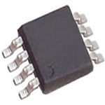
ICGOO电子元器件商城为您提供SSM2301RMZ-REEL7由Analog设计生产,在icgoo商城现货销售,并且可以通过原厂、代理商等渠道进行代购。 SSM2301RMZ-REEL7价格参考¥2.60-¥8.32。AnalogSSM2301RMZ-REEL7封装/规格:线性 - 音頻放大器, Amplifier IC 1-Channel (Mono) Class D 8-MSOP。您可以下载SSM2301RMZ-REEL7参考资料、Datasheet数据手册功能说明书,资料中有SSM2301RMZ-REEL7 详细功能的应用电路图电压和使用方法及教程。
Analog Devices Inc.(ADI公司)的SSM2301RMZ-REEL7是一款用于音频应用的线性音频放大器。这款器件特别适用于便携式设备和低功耗应用场景,如手机、平板电脑、便携式媒体播放器、蓝牙音箱等。

 主要应用场景:

1. 便携式音频设备:
   - SSM2301RMZ-REEL7非常适合用于便携式音频设备,因为它具有低功耗特性,能够在电池供电的情况下长时间工作。例如,在智能手机和平板电脑中,它可以驱动内置扬声器或外部耳机,提供清晰的音频输出。

2. 蓝牙音箱和无线音频设备:
   - 在蓝牙音箱和其他无线音频设备中,SSM2301RMZ-REEL7能够提供高效且高质量的音频放大功能。它的低失真和高信噪比特性确保了音质的纯净,同时其低功耗设计延长了电池寿命。

3. 智能家居设备:
   - 在智能家居设备中,如智能音箱、智能门铃等,SSM2301RMZ-REEL7可以用来驱动内置扬声器,提供清晰的语音提示或音乐播放功能。它的小尺寸封装使其易于集成到紧凑的设计中。

4. 便携式医疗设备:
   - 对于一些便携式医疗设备,如助听器、心率监测仪等,SSM2301RMZ-REEL7可以用于音频反馈或语音提示功能。它的低功耗和小尺寸特性使得它成为这些设备的理想选择。

5. 汽车音响系统:
   - 在汽车音响系统中,尤其是那些注重低功耗和空间利用的紧凑型车辆中,SSM2301RMZ-REEL7可以用于驱动车内扬声器,提供良好的音频体验。它的小尺寸和高效能使其适合安装在空间有限的环境中。

 特点总结:
- 低功耗:适合电池供电的应用场景,延长设备的续航时间。
- 高效率:采用Class D架构,提高能量转换效率,减少热量产生。
- 低失真:提供高质量的音频输出,保持音质的纯净。
- 小尺寸封装:便于集成到各种紧凑型设备中。
- 高信噪比:确保音频信号的清晰度,减少背景噪音。

总之,SSM2301RMZ-REEL7凭借其低功耗、高效能和高音质的特点,广泛应用于各类便携式音频设备和低功耗应用场景中。
| 参数 | 数值 |
| 产品目录 | 集成电路 (IC)半导体 |
| 描述 | IC AMP AUDIO 1.52W MONO D 8MSOP音频放大器 Filterless Hi Eff Mono 1.4 W Class-D |
| 产品分类 | |
| 品牌 | Analog Devices |
| 产品手册 | |
| 产品图片 |
|
| rohs | 符合RoHS无铅 / 符合限制有害物质指令(RoHS)规范要求 |
| 产品系列 | 音频 IC,音频放大器,Analog Devices SSM2301RMZ-REEL7- |
| 数据手册 | |
| 产品型号 | SSM2301RMZ-REEL7 |
| THD+噪声 | 0.1 % |
| 不同负载时的最大输出功率x通道数 | 1.52W x 1 @ 8 欧姆 |
| 产品 | Class-D |
| 产品目录页面 | |
| 产品种类 | 音频放大器 |
| 供应商器件封装 | 8-MSOP |
| 共模抑制比—最小值 | 55 dB |
| 其它名称 | SSM2301RMZ-REEL7CT |
| 包装 | 剪切带 (CT) |
| 商标 | Analog Devices |
| 增益 | 6 dB |
| 安装类型 | 表面贴装 |
| 安装风格 | SMD/SMT |
| 封装 | Reel |
| 封装/外壳 | 8-TSSOP,8-MSOP(0.118",3.00mm 宽) |
| 封装/箱体 | MSOP-8 |
| 工作温度 | -40°C ~ 85°C (TA) |
| 工作电源电压 | 2.5 V to 5 V |
| 工厂包装数量 | 1000 |
| 最大工作温度 | + 85 C |
| 最小工作温度 | - 40 C |
| 标准包装 | 1 |
| 特性 | 消除爆音,差分输入,短路和热保护,关闭 |
| 电压-电源 | 2.5 V ~ 5 V |
| 电源电压-最大 | 5 V |
| 电源电压-最小 | 2.5 V |
| 电源电流 | 4.2 mA |
| 电源类型 | Single |
| 类型 | 1-Channel Mono |
| 系列 | SSM2301 |
| 输入信号类型 | Differential |
| 输出功率 | 1.4 W |
| 输出类型 | 1-通道(单声道) |
| 配用 | /product-detail/zh/SSM2301-MINI-EVALZ/SSM2301-MINI-EVALZ-ND/1873728 |


- 商务部:美国ITC正式对集成电路等产品启动337调查
- 曝三星4nm工艺存在良率问题 高通将骁龙8 Gen1或转产台积电
- 太阳诱电将投资9.5亿元在常州建新厂生产MLCC 预计2023年完工
- 英特尔发布欧洲新工厂建设计划 深化IDM 2.0 战略
- 台积电先进制程称霸业界 有大客户加持明年业绩稳了
- 达到5530亿美元!SIA预计今年全球半导体销售额将创下新高
- 英特尔拟将自动驾驶子公司Mobileye上市 估值或超500亿美元
- 三星加码芯片和SET,合并消费电子和移动部门,撤换高东真等 CEO
- 三星电子宣布重大人事变动 还合并消费电子和移动部门
- 海关总署:前11个月进口集成电路产品价值2.52万亿元 增长14.8%


PDF Datasheet 数据手册内容提取
Filterless High Efficiency Mono 1.4 W Class-D Audio Amplifier SSM2301 FEATURES The SSM2301 operates with 85% efficiency at 1.4 W into 8 Ω Filterless Class-D amplifier with Σ-Δ modulation from a 5.0 V supply and has a signal-to-noise ratio (SNR) that No sync necessary when using multiple Class-D amplifiers is greater than 98 dB. Spread-spectrum modulation is used to from Analog Devices, Inc. provide lower EMI-radiated emissions compared with other 1.4 W into 8 Ω at 5.0 V supply with less than 1% THD + N Class-D architectures. 85% efficiency at 5.0 V, 1.4 W into 8 Ω speaker The SSM2301 has a micropower shutdown mode with a maximum Greater than 98 dB SNR (signal-to-noise ratio) shutdown current of 30 nA. Shutdown is enabled by applying Single-supply operation from 2.5 V to 5.0 V a logic low to the SD pin. 20 nA ultralow shutdown current Short-circuit and thermal protection The device also includes pop-and-click suppression circuitry. Available in 8-lead, 3 mm × 3 mm LFCSP and MSOP packages This minimizes voltage glitches at the output during turn-on Pop-and-click suppression and turn-off, thus reducing audible noise on activation and Built-in resistors reduce board component count deactivation. Fixed and user-adjustable gain configurations APPLICATIONS The fully differential input of the SSM2301 provides excellent rejection of common-mode noise on the input. Input coupling Mobile phones capacitors can be omitted if the dc input common-mode voltage MP3 players is approximately V /2. Portable gaming DD Portable electronics The SSM2301 also has excellent rejection of power supply noise, Educational toys including noise caused by GSM transmission bursts and RF GENERAL DESCRIPTION rectification. PSRR is typically 63 dB at 217 Hz. The SSM2301 is a fully integrated, high efficiency, Class-D audio The gain can be set to 6 dB or 12 dB by utilizing the gain control amplifier designed to maximize performance for mobile phone select pin connected respectively to ground or to VDD. Gain applications. The application circuit requires a minimum of can also be adjusted externally by inserting a resistor in series external components and operates from a single 2.5 V to 5.0 V with each input pin. supply. It is capable of delivering 1.4 W of continuous output power with less than 1% THD + N driving an 8 Ω load from The SSM2301 is specified over the commercial temperature range a 5.0 V supply. (−40°C to +85°C). It has built-in thermal shutdown and output short-circuit protection. It is available in both an 8-lead, 3 mm × The SSM2301 features a high efficiency, low noise modulation 3 mm lead-frame chip scale package (LFCSP) and an 8-lead scheme that does not require external LC output filters. The modu- MSOP package. lation provides high efficiency even at low output power. FUNCTIONAL BLOCK DIAGRAM 10µF VBATT 2.5V TO 5.0V 0.1µF SSM2301 VDD 0.01µF1 IN+ OUT+ AUDIO IN+ GAIN FET IN– CONTROL MODULATOR DRIVER OUT– AUDIO IN– 0.01µF1 GAIN SHUTDOWN SD BIAS OSCILLATOR SUPPOPPR/CELSISCIKON GND N1IVONOTPLEUTSTA CGAEP ISS AARPEP ROOPXTIIMOANTAELL IYF VINDPDU/2T. DC COMMON-MODE 06163-001 Figure 1. Rev. A Information furnished by Analog Devices is believed to be accurate and reliable. However, no responsibility is assumed by Analog Devices for its use, nor for any infringements of patents or other One Technology Way, P.O. Box 9106, Norwood, MA 02062-9106, U.S.A. rights of third parties that may result from its use. Specifications subject to change without notice. No license is granted by implication or otherwise under any patent or patent rights of Analog Devices. Tel: 781.329.4700 www.analog.com Trademarks and registered trademarks are the property of their respective owners. Fax: 781.461.3113 ©2007 Analog Devices, Inc. All rights reserved.
SSM2301 TABLE OF CONTENTS Features..............................................................................................1 Typical Application Circuits.........................................................10 Applications.......................................................................................1 Applications Information..............................................................12 General Description.........................................................................1 Overview.....................................................................................12 Functional Block Diagram..............................................................1 Gain Selection.............................................................................12 Revision History...............................................................................2 Pop-and-Click Suppression......................................................12 Specifications.....................................................................................3 Layout..........................................................................................12 Absolute Maximum Ratings............................................................4 Input Capacitor Selection..........................................................12 Thermal Resistance......................................................................4 Proper Power Supply Decoupling............................................13 ESD Caution..................................................................................4 Outline Dimensions.......................................................................14 Pin Configurations and Function Descriptions...........................5 Ordering Guide..........................................................................14 Typical Performance Characteristics.............................................6 REVISION HISTORY 10/07—Rev. 0 to Rev. A Added MSOP Package.......................................................Universal Changes to Features..........................................................................1 Changes to General Description....................................................1 Changes to Table 1............................................................................3 Deleted Evaluation Board Information Section.........................14 Updated Outline Dimensions.......................................................14 Changes to Ordering Guide..........................................................14 1/07—Revision 0: Initial Version Rev. A | Page 2 of 16
SSM2301 SPECIFICATIONS V = 5.0 V, T = 25oC, R = 8 Ω + 33 μH, unless otherwise noted. DD A L Table 1. Parameter Symbol Conditions Min Typ Max Unit DEVICE CHARACTERISTICS Output Power P V = 5.0 V, R = 8 Ω, THD = 1% 1.22 W O DD L f = 1 kHz, 20 kHz BW V = 5.0 V, R = 8 Ω, THD = 10% 1.52 W DD L f = 1 kHz, 20 kHz BW V = 3.6 V, R = 8 Ω, THD = 1% 590 mW DD L f = 1 kHz, 20 kHz BW V = 3.6 V, R = 8 Ω, THD = 10% 775 mW DD L f = 1 kHz, 20 kHz BW V = 2.5 V, R = 8 Ω, THD = 1% 275 mW DD L f = 1 kHz, 20 kHz BW V = 2.5 V, R = 8 Ω, THD = 10% 345 mW DD L f = 1 kHz, 20 kHz BW Efficiency η P = 1.4 W, 8 Ω, V = 5.0 V 85 % OUT DD Total Harmonic Distortion + Noise THD + N P = 1 W into 8 Ω, f = 1 kHz, V = 5.0 V 0.1 % O DD P = 0.5 W into 8 Ω, f = 1 kHz, V = 3.6 V 0.04 % O DD Input Common-Mode Voltage Range V 1.0 V − 1.0 V CM DD Common-Mode Rejection Ratio CMRR V = 2.5 V ± 100 mV at 217 Hz 55 dB GSM CM Average Switching Frequency f 1.8 MHz SW Differential Output Offset Voltage V G = 6 dB; G = 12 dB 2.0 mV OOS POWER SUPPLY Supply Voltage Range V Guaranteed from PSRR test 2.5 5.0 V DD Power Supply Rejection Ratio PSRR V = 2.5 V to 5.0 V, dc input floating/ground 70 85 dB DD PSRR V = 100 mV at 217 Hz, inputs are ac grounded, 63 dB GSM RIPPLE C = 0.01 μF, input referred IN Supply Current I V = 0 V, no load, V = 5.0 V 4.2 mA SY IN DD V = 0 V, no load, V = 3.6 V 3.5 mA IN DD V = 0 V, no load, V = 2.5 V 2.9 mA IN DD Shutdown Current I SD = GND 20 nA SD GAIN CONTROL Closed-Loop Gain A 0 GAIN pin = 0 V 6 dB V A 1 GAIN pin = V 12 dB V DD Differential Input Impedance Z SD = V , SD = GND 150 kΩ IN DD 210 kΩ SHUTDOWN CONTROL Input Voltage High V I ≥ 1 mA 1.2 V IH SY Input Voltage Low V I ≤ 300 nA 0.5 V IL SY Turn-On Time t SD rising edge from GND to V 30 ms WU DD Turn-Off Time t SD falling edge from V to GND 5 μs SD DD Output Impedance Z SD = GND >100 kΩ OUT NOISE PERFORMANCE Output Voltage Noise e V = 2.5 V to 5.0 V, f = 20 Hz to 20 kHz, inputs are 35 μV n DD ac grounded, sine wave, A = 6 dB, A weighting V Signal-to-Noise Ratio SNR P = 1.4 W, R = 8 Ω 98 dB OUT L Rev. A | Page 3 of 16
SSM2301 ABSOLUTE MAXIMUM RATINGS Absolute maximum ratings apply at 25°C, unless otherwise noted. THERMAL RESISTANCE θ is specified for the worst-case conditions, that is, a device JA Table 2. soldered in a circuit board for surface-mount packages. Parameter Rating Supply Voltage 6 V Table 3. Thermal Resistance Input Voltage VDD Package Type θJA θJC Unit Common-Mode Input Voltage V DD 8-lead, 3 mm × 3 mm LFCSP 62 20.8 °C/W Storage Temperature Range −65°C to +150°C 8-lead MSOP 210 45 °C/W Operating Temperature Range −40°C to +85°C Junction Temperature Range −65°C to +165°C ESD CAUTION Lead Temperature (Soldering, 60 sec) 300°C Stresses above those listed under Absolute Maximum Ratings may cause permanent damage to the device. This is a stress rating only; functional operation of the device at these or any other conditions above those indicated in the operational section of this specification is not implied. Exposure to absolute maximum rating conditions for extended periods may affect device reliability. Rev. A | Page 4 of 16
SSM2301 PIN CONFIGURATIONS AND FUNCTION DESCRIPTIONS PIN 1 SD 1 INDICATOR 8 OUT– SD 1 8 OUT– GAIN 2 SSM2301 7 GND GAIN 2 SSM2301 7 GND IINN+– 34 (NToOt Pto V SIEcaWle) 65 VODUDT+ 06163-002 IINN+– 34 (NToOt Pto V SIEcaWle) 65 VODUDT+ 06163-103 Figure 2. LFCSP Pin Configuration Figure 3. MSOP Pin Configuration Table 4. Pin Function Descriptions Pin No. Mnemonic Description 1 SD Shutdown Input. Active low digital input. 2 GAIN Gain Selection. Digital input. 3 IN+ Noninverting Input. 4 IN− Inverting Input. 5 OUT+ Noninverting Output. 6 VDD Power Supply. 7 GND Ground. 8 OUT− Inverting Output. Rev. A | Page 5 of 16
SSM2301 TYPICAL PERFORMANCE CHARACTERISTICS 100 100 RL = 8Ω, 15µH VDD = 5.0V GAIN = 6dB GAIN = 12dB 10 RL = 8Ω, 15µH 10 VDD = 2.5V 1 %) %) N ( VDD = 3.6V N ( 0.5W 1W + 1 + 0.1 D D H H T T 0.25W 0.01 0.1 0.001 VDD = 5V 0.01 0.0001 0.0001 0.001 OU0.T0P1UT POWE0R.1 (W) 1 10 06163-004 10 100 FREQUE1NkCY (Hz) 10k 100k 06163-008 Figure 4. THD + N vs. Output Power into 8 Ω, AV = 6 dB Figure 7. THD + N vs. Frequency, VDD = 5.0 V, AV = 12 dB, RL = 8 Ω 100 100 RL = 8Ω, 15µH VDD = 3.6V GAIN = 12dB GAIN = 6dB 10 RL = 8Ω, 15µH 10 VDD = 2.5V 1 N (%) VDD = 3.6V N (%) 0.5W D + 1 D + 0.1 0.25W H H T T 0.01 0.125W 0.1 0.001 VDD = 5V 0.01 0.0001 0.0001 0.001 OU0.T0P1UT POWE0R.1 (W) 1 10 06163-003 10 100 FREQUE1NkCY (Hz) 10k 100k 06163-009 Figure 5. THD + N vs. Output Power into 8 Ω, AV = 12 dB Figure 8. THD + N vs. Frequency, VDD = 3.6 V, AV = 6 dB, RL = 8 Ω 100 100 VDD = 5.0V VDD = 3.6V GAIN = 6dB GAIN = 12dB 10 RL = 8Ω, 15µH 10 RL = 8Ω, 15µH 1 1 %) %) 0.5W N ( 0.5W 1W N ( + 0.1 + 0.1 0.25W D D H H T T 0.125W 0.01 0.25W 0.01 0.001 0.001 0.0001 0.0001 10 100 FREQUE1NkCY (Hz) 10k 100k 06163-007 10 100 FREQUE1NkCY (Hz) 10k 100k 06163-010 Figure 6. THD + N vs. Frequency, VDD = 5.0 V, AV = 6 dB, RL = 8 Ω Figure 9. THD + N vs. Frequency, VDD = 3.6 V, AV = 12 dB, RL = 8 Ω Rev. A | Page 6 of 16
SSM2301 100 12 VDD = 2.5V GAIN = 6dB 10 RL = 8Ω, 15µH 10 A) µ 1 T ( 8 %) 0.25W REN VDD = 5.0V + N ( 0.1 0.125W CUR 6 HD WN VDD = 2.5V T 0.075W O 0.01 TD 4 U SH VDD = 3.6V 0.001 2 0.0001 0 10 100 FREQUE1NkCY (Hz) 10k 100k 06163-011 0 0.1 0.2 SHU0T.3DOWN0 .V4OLTA0G.5E (V)0.6 0.7 0.8 06163-020 Figure 10. THD + N vs. Frequency, VDD = 2.5 V, AV = 6 dB, RL = 8 Ω Figure 13. Shutdown Current vs. Shutdown Voltage 100 1.6 VDD = 2.5V f = 1kHz GAIN = 12dB GAIN = 6dB 10 RL = 8Ω, 15µH 1.4 RL = 8Ω 1.2 D + N (%) 0.11 000...01272555WWW T POWER (W) 10..08 10% H U 1% T TP 0.6 0.01 U O 0.4 0.001 0.2 0.0001 0 10 100 FREQUE1NkCY (Hz) 10k 100k 06163-012 2.5 3.0 SUP3P.5LY VOLTA4G.0E (V) 4.5 5.0 06163-021 Figure 11. THD + N vs. Frequency, VDD = 2.5 V, AV = 12 dB, RL = 8 Ω Figure 14. Maximum Output Power vs. Supply Voltage, AV = 6 dB, RL = 8 Ω, 5.0 1.8 f = 1kHz 4.5 1.6 GRLA I=N 8 =Ω 12dB 4.0 1.4 mA) 3.5 W) 1.2 NT ( 3.0 ER ( E W 1.0 CURR 2.5 T PO 0.8 10% UPPLY 21..05 OUTPU 0.6 1% S 0.4 1.0 0.5 0.2 0 0 2.5 3.0 3S.5UPPLY V4O.0LTAGE (4V.)5 5.0 5.5 06163-019 2.5 3.0 SUP3P.5LY VOLTA4G.0E (V) 4.5 5.0 06163-022 Figure 12. Supply Current vs. Supply Voltage, No Load Figure 15. Maximum Output Power vs. Supply Voltage, AV = 12 dB, RL = 8 Ω Rev. A | Page 7 of 16
SSM2301 100 400 VDD = 3.6V RL = 8Ω, 15µH RL = 8Ω, 15µH 90 350 80 VDD = 2.5V VDD = 5.0V 300 Y (%) 6700 VDD = 5.0V ENT (mA) 250 VDD = 3.6V C R EN 50 UR 200 FICI 40 Y C VDD = 2.5V F L 150 E P P 30 U S 100 20 50 10 0 0 0 0.2 0.4 OU0T.P6UT PO0W.8ER (W1).0 1.2 1.4 06163-025 0 0.1 0.2 0.3 0.4 0.O5U0T.P6U0T. 7PO0W.8E0R.9 (W1).0 1.1 1.2 1.3 1.4 1.5 06163-031 Figure 16. Efficiency vs. Output Power into 8 Ω Figure 19. Supply Current vs. Output Power into 8 Ω, One Channel 0.20 0 VDD = 3.6V 0.18 RL = 8Ω, 15µH –10 0.16 –20 W) N ( 0.14 –30 O SIPATI 00..1102 R (dB) ––4500 S R R DI 0.08 PS –60 E OW 0.06 –70 P 0.04 –80 0.02 –90 0 –100 0 0.1 0.2 O0U.3TPUT 0P.O4WER0 (.W5) 0.6 0.7 0.806163-050 10 100 FREQUE1NkCY (Hz) 10k 100k 06163-033 Figure 17. Power Dissipation vs. Output Power into 8 Ω at VDD = 3.6 V Figure 20. Power Supply Rejection Ratio vs. Frequency 0.30 0 VDD = 5.0V RL = 8Ω, 33µH RL = 8Ω, 15µH –10 GAIN = 6dB 0.25 W) –20 N ( 0.20 O –30 SIPATI 0.15 R (dB) –40 S R DI M R C –50 WE 0.10 O P –60 0.05 –70 0 –80 0 0.1 0.2 0.3 0.4 0.O5U0T.6PU0T.7 PO0.W8E0R.9 (W1.)0 1.1 1.2 1.3 1.4 1.506163-051 10 100 FREQUE1NkCY (Hz) 10k 100k 06163-034 Figure 18. Power Dissipation vs. Output Power into 8 Ω at VDD = 5.0 V Figure 21. Common-Mode Rejection Ratio vs. Frequency Rev. A | Page 8 of 16
SSM2301 7 7 6 6 OUTPUT 5 5 SD INPUT 4 4 V) SD INPUT V) E ( 3 E ( 3 G G A A LT 2 LT 2 O O V V 1 OUTPUT 1 0 0 –1 –1 –2 –2 –10–5 0 5 1015202530T3I5ME40 (m45s)505560657075808590 06163-035 –20 0 20 40 60TIME80 (ms)100 120 140 160 180 06163-036 Figure 22. Turn-On Response Figure 23. Turn-Off Response Rev. A | Page 9 of 16
SSM2301 TYPICAL APPLICATION CIRCUITS 0.1µF 10µF VBATT 2.5V TO 5.0V SSM2301 VDD 0.01µF1 IN+ OUT+ AUDIO IN+ GAIN FET IN– CONTROL MODULATOR DRIVER OUT– AUDIO IN– VDD 0.01µF1 GAIN SHUTDOWN SD BIAS OSCILLATOR SUPPOPPR/CELSISCIKON GND N1IVONOTPLEUTSTA CGAEP IASC AITPOPRROS XAIRMEA TOEPLTYIO VNDAD/L2 .IF INPUT DC COMMON-MODE 06163-037 Figure 24. Differential Input Configuration, Gain = 12 dB 0.1µF 10µF VBATT 2.4V TO 5.0V SSM2301 VDD 0.01µF IN+ OUT+ AUDIO IN GAIN FET IN– CONTROL MODULATOR DRIVER OUT– 0.01µF GAIN SHUTDOWN SD BIAS OSCILLATOR SUPPOPPR/CELSISCIKON GND 06163-038 Figure 25. Single-Ended Input Configuration, Gain = 6 dB EXTERNAL GAIN SETTINGS = 20 log[4/(1 + R/150kΩ)] 0.1µF 10µF VBATT 2.4V TO 5.0V SSM2301 VDD 0.01µF1 R IN+ OUT+ AUDIO IN+ GAIN FET R IN– CONTROL MODULATOR DRIVER OUT– AUDIO IN– 0.01µF1 VDD GAIN SHUTDOWN SD BIAS OSCILLATOR SUPPOPPR/CELSISCIKON GND N1IVONOTPLEUTSTA CGAEP IASC AITPOPRROS XAIRMEA TOEPLTYIO VNDAD/L2 .IF INPUT DC COMMON-MODE 06163-039 Figure 26. Differential Input Configuration, User-Adjustable Gain Rev. A | Page 10 of 16
SSM2301 EXTERNAL GAIN SETTINGS = 20 log[4/(1 + R/150kΩ)] 0.1µF 10µF VBATT 2.4V TO 5.0V SSM2301 VDD 0.01µF R IN+ OUT+ AUDIO IN GAIN FET R IN– CONTROL MODULATOR DRIVER OUT– 0.01µF VDD GAIN SHUTDOWN SD BIAS OSCILLATOR SUPPOPPR/CELSISCIKON GND 06163-040 Figure 27. Single-Ended Input Configuration, User-Adjustable Gain EXTERNAL GAIN SETTINGS = 20 log[2/(1 + R/150kΩ)] 0.1µF 10µF VBATT 2.4V TO 5.0V SSM2301 VDD 0.01µF1 R IN+ OUT+ AUDIO IN+ GAIN FET R IN– CONTROL MODULATOR DRIVER OUT– AUDIO IN– 0.01µF1 GAIN SHUTDOWN SD BIAS OSCILLATOR SUPPOPPR/CELSISCIKON GND N1IVONOTPLEUTSTA CGAEP IASC AITPOPRROS XAIRMEA TOEPLTYIO VNDAD/L2 .IF INPUT DC COMMON-MODE 06163-041 Figure 28. Differential Input Configuration, User-Adjustable Gain EXTERNAL GAIN SETTINGS = 20 log[2/(1 + R/150kΩ)] 0.1µF 10µF VBATT 2.4V TO 5.0V SSM2301 VDD 0.01µF R IN+ OUT+ AUDIO IN GAIN FET IN– CONTROL MODULATOR DRIVER OUT– 0.01µF R GAIN SHUTDOWN SD BIAS OSCILLATOR SUPPOPPR/CELSISCIKON GND 06163-042 Figure 29. Single-Ended Input Configuration, User-Adjustable Gain Rev. A | Page 11 of 16
SSM2301 APPLICATIONS INFORMATION OVERVIEW LAYOUT The SSM2301 mono Class-D audio amplifier features a filterless As output power continues to increase, care must be taken to modulation scheme that greatly reduces external component count, lay out PCB traces and wires properly between the amplifier, conserving board space and, thus, reducing system cost. The load, and power supply. A good practice is to use short, wide SSM2301 does not require an output filter but, instead, relies PCB tracks to decrease voltage drops and minimize inductance. on the inherent inductance of the speaker coil and the natural Make track widths at least 200 mil for every inch of track length filtering of the speaker and human ear to fully recover the audio for lowest DCR, and use 1 oz or 2 oz of copper PCB traces to component of the square-wave output. While most Class-D ampli- further reduce IR drops and inductance. fiers use some variation of pulse-width modulation (PWM), the Poor layout increases voltage drops, consequently affecting SSM2301 uses a Σ-Δ modulation to determine the switching efficiency. Use large traces for the power supply inputs and pattern of the output devices. This provides a number of important amplifier outputs to minimize losses due to parasitic trace benefits. Σ-Δ modulators do not produce a sharp peak with many resistance. Proper grounding guidelines help improve audio harmonics in the AM frequency band, as pulse-width modulators performance, minimize crosstalk between channels, and prevent often do. Σ-Δ modulation reduces the amplitude of spectral switching noise from coupling into the audio signal. To maintain components at high frequencies, thereby reducing EMI emission high output swing and high peak output power, PCB traces that that might otherwise be radiated by speakers and long cable traces. connect the output pins to the load and supply pins should be The SSM2301 also offers protection circuitry for output short- as wide as possible to maintain the minimum trace resistances. circuit and high temperature conditions. When the fault-inducing condition is removed, the SSM2301 automatically recovers It is also recommended that a large-area ground plane be used for without the need for a hard reset. minimum impedances. Good PCB layouts also isolate critical GAIN SELECTION analog paths from sources of high interference. High frequency circuits (analog and digital) should be separated from low Pulling the GAIN pin of the SSM2301 high sets the gain of the frequency circuits. Properly designed multilayer printed circuit speaker amplifier to 12 dB; pulling it low sets the gain of the boards can reduce EMI emission and increase immunity to the speaker amplifier to 6 dB. RF field by a factor of 10 or more compared with double-sided boards. A multilayer board allows a complete layer to be used It is possible to adjust the SSM2301 gain by using external resistors for the ground plane, whereas the ground plane side of a double- at the input. To set a gain lower than 12 dB, see Figure 26 for side board is often disrupted with signal crossover. If the system differential input configuration and Figure 27 for single-ended has separate analog and digital ground and power planes, the configuration. For external gain configuration from a fixed 12 dB analog ground plane should be underneath the analog power plane, gain, use the following formula: and, similarly, the digital ground plane should be underneath the External Gain Settings = 20 log[4/(1 + R/150 kΩ)] digital power plane. There should be no overlap between analog and digital ground planes or analog and digital power planes. To set a gain lower than 6 dB, see Figure 28 for differential input configuration and Figure 29 for single-ended configuration. For INPUT CAPACITOR SELECTION external gain configuration from a fixed 6 dB gain, use the The SSM2301 does not require input coupling capacitors if the following formula: input signal is biased from 1.0 V to V − 1.0 V. Input capacitors DD External Gain Settings = 20 log[2/(1 + R/150 kΩ)] are required if the input signal is not biased within this recom- POP-AND-CLICK SUPPRESSION mended input dc common-mode voltage range, if high-pass filtering is needed (see Figure 24) or if using a single-ended Voltage transients at the output of audio amplifiers may occur source (see Figure 25). If high-pass filtering is needed at the input, when shutdown is activated or deactivated. Voltage transients the input capacitor, along with the input resistor of the SSM2301, as low as 10 mV can be heard as an audio pop in the speaker. forms a high-pass filter whose corner frequency is determined Clicks and pops can also be classified as undesirable audible by the following equation: transients generated by the amplifier system and, therefore, f = 1/(2π × R × C ) as not coming from the system input signal. Such transients may C IN IN be generated when the amplifier system changes its operating The input capacitor can have very important effects on the mode. For example, the following can be sources of audible circuit performance. Not using input capacitors degrades the transients: system power-up/power-down, mute/unmute, input output offset of the amplifier as well as the PSRR performance. source change, and sample rate change. The SSM2301 has a pop- and-click suppression architecture that reduces these output transients, resulting in noiseless activation and deactivation. Rev. A | Page 12 of 16
SSM2301 PROPER POWER SUPPLY DECOUPLING The power supply input needs to be decoupled with a good To ensure high efficiency, low total harmonic distortion (THD), quality low ESL and low ESR capacitor, usually around 4.7 μF. and high PSRR, proper power supply decoupling is necessary. This capacitor bypasses low frequency noises to the ground Noise transients on the power supply lines are short-duration plane. For high frequency transients noises, use a 0.1 μF voltage spikes. Although the actual switching frequency can capacitor placed as close as possible to the VDD pin of the range from 10 kHz to 100 kHz, these spikes can contain frequency device. Placing the decoupling capacitor as close as possible components that extend into the hundreds of megahertz. to the SSM2301 helps maintain efficient performance. Rev. A | Page 13 of 16
SSM2301 OUTLINE DIMENSIONS 0.50 0.40 3.00 0.60 MAX 0.30 PIN 1 BSC SQ INDICATOR 1 8 PIN 1 2.75 1.89 INDICATOR VTIOEWP BSC SQ 1R.E5F0 1.74 0.50 1.59 BSC 5 4 1.60 0.90 MAX 12° MAX 00..6750 TMYAPX 11..4350 0.85 NOM 0.05 MAX 0.01 NOM SEATING 0.30 0.20 REF PLANE 0.23 0.18 Figure 30. 8-Lead Lead Frame Chip Scale Package [LFCSP_VD] 3 mm × 3 mm Body, Very Thin, Dual Lead (CP-8-2) Dimensions shown in millimeters 3.20 3.00 2.80 8 5 5.15 3.20 4.90 3.00 4.65 2.80 1 4 PIN 1 0.65 BSC 0.95 0.85 1.10 MAX 0.75 0.80 0.15 0.38 0.23 8° 0.60 0.00 0.22 0.08 0° 0.40 COPLANARITY SEATING 0.10 PLANE COMPLIANT TO JEDEC STANDARDS MO-187-AA Figure 31. 8-Lead Mini Small Outline Package [MSOP] (RM-8) Dimensions shown in millimeters ORDERING GUIDE Temperature Package Model Range Package Description Option Branding SSM2301CPZ-R21 −40°C to +85°C 8-Lead Lead Frame Chip Scale Package [LFCSP_VD] CP-8-2 A1C SSM2301CPZ-REEL1 −40°C to +85°C 8-Lead Lead Frame Chip Scale Package [LFCSP_VD] CP-8-2 A1C SSM2301CPZ-REEL71 −40°C to +85°C 8-Lead Lead Frame Chip Scale Package [LFCSP_VD] CP-8-2 A1C SSM2301RMZ-R21 −40°C to +85°C 8-Lead Mini Small Outline Package [MSOP] RM-8 A1C SSM2301RMZ-REEL1 −40°C to +85°C 8-Lead Mini Small Outline Package [MSOP] RM-8 A1C SSM2301RMZ-REEL71 −40°C to +85°C 8-Lead Mini Small Outline Package [MSOP] RM-8 A1C SSM2301-EVALZ1 Evaluation Board with LFCSP Model 1 Z = RoHS Compliant Part. Rev. A | Page 14 of 16
SSM2301 NOTES Rev. A | Page 15 of 16
SSM2301 NOTES ©2007 Analog Devices, Inc. All rights reserved. Trademarks and registered trademarks are the property of their respective owners. D06163-0-10/07(A) Rev. A | Page 16 of 16