ICGOO在线商城 > MAX5309EUE+

 Datasheet下载
- 型号: MAX5309EUE+
- 制造商: Maxim
- 库位|库存: xxxx|xxxx
- 要求:
| 数量阶梯 | 香港交货 | 国内含税 |
| +xxxx | $xxxx | ¥xxxx |
查看当月历史价格
查看今年历史价格
MAX5309EUE+产品简介:
ICGOO电子元器件商城为您提供MAX5309EUE+由Maxim设计生产,在icgoo商城现货销售,并且可以通过原厂、代理商等渠道进行代购。 提供MAX5309EUE+价格参考以及MaximMAX5309EUE+封装/规格参数等产品信息。 你可以下载MAX5309EUE+参考资料、Datasheet数据手册功能说明书, 资料中有MAX5309EUE+详细功能的应用电路图电压和使用方法及教程。
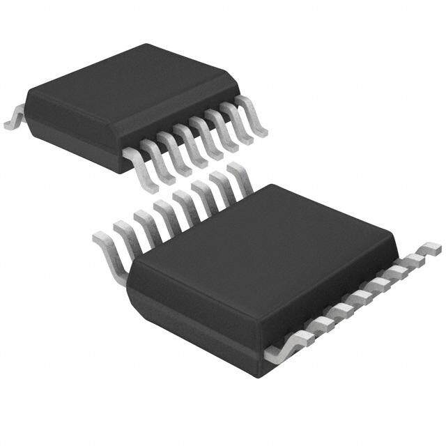
Maxim Integrated的MAX5309EUE+是一款双通道、低功耗、12位数模转换器(DAC),采用16引脚TSSOP封装。该器件内置基准电压源,支持单电源供电(2.7V至5.5V),具有良好的精度和稳定性,适用于对空间和功耗敏感的应用场景。

典型应用场景包括:
1. 工业控制与自动化:用于PLC(可编程逻辑控制器)、传感器校准和执行器控制中,提供精确的模拟电压输出,实现对温度、压力、流量等参数的调节。
2. 便携式设备:因其低功耗特性,广泛应用于电池供电设备,如手持测试仪器、医疗监控设备和移动数据采集系统。
3. 通信系统:在光模块或射频前端中用于偏置电压调节、增益控制等模拟信号调理功能。
4. 消费电子与嵌入式系统:适用于需要多路模拟输出的音频设备、显示亮度调节或自动校准电路。
5. 测试与测量设备:作为信号发生器或校准源的一部分,生成精确的直流或低频模拟信号。

MAX5309EUE+通过I²C接口与主控制器通信,支持标准和快速模式(最高400kHz),便于集成到现有系统中。其内置上电复位功能确保输出稳定,避免启动时的电压突变,提高系统可靠性。整体设计简洁,外围元件少,适合高密度PCB布局,是中小精度模拟输出需求的理想选择。
| 参数 | 数值 |
| 产品目录 | 集成电路 (IC)半导体 |
| 描述 | IC DAC 10BIT OCT LP SER 16-TSSOP数模转换器- DAC 10-Bit 8Ch Precision DAC |
| 产品分类 | |
| 品牌 | Maxim Integrated |
| 产品手册 | |
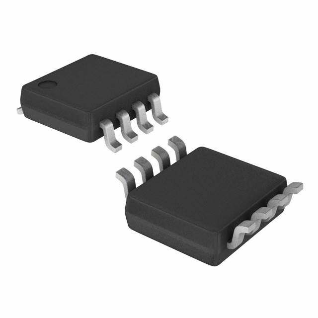
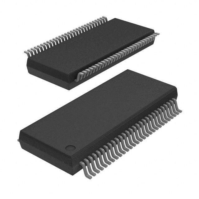
| 产品图片 |
|
| rohs | 符合RoHS无铅 / 符合限制有害物质指令(RoHS)规范要求 |
| 产品系列 | 数据转换器IC,数模转换器- DAC,Maxim Integrated MAX5309EUE+- |
| 数据手册 | |
| 产品型号 | MAX5309EUE+ |
| 产品培训模块 | http://www.digikey.cn/PTM/IndividualPTM.page?site=cn&lang=zhs&ptm=25703http://www.digikey.cn/PTM/IndividualPTM.page?site=cn&lang=zhs&ptm=25705 |
| 产品种类 | 数模转换器- DAC |
| 位数 | 10 |
| 供应商器件封装 | 16-TSSOP |
| 分辨率 | 10 bit |
| 包装 | 管件 |
| 商标 | Maxim Integrated |
| 安装类型 | 表面贴装 |
| 安装风格 | SMD/SMT |
| 封装 | Tube |
| 封装/外壳 | 16-TSSOP(0.173",4.40mm 宽) |
| 封装/箱体 | TSSOP-16 |
| 工作温度 | -40°C ~ 85°C |
| 工厂包装数量 | 96 |
| 建立时间 | 5µs |
| 接口类型 | QSPI, SPI, Serial (3-Wire, Microwire) |
| 数据接口 | 串行 |
| 最大工作温度 | + 85 C |
| 最小工作温度 | - 40 C |
| 标准包装 | 1 |
| 电压参考 | External |
| 电压源 | 单电源 |
| 电源电压-最大 | 5.5 V |
| 电源电压-最小 | 2.7 V |
| 积分非线性 | +/- 2 LSB |
| 稳定时间 | 5 us |
| 系列 | MAX5309 |
| 转换器数 | 8 |
| 转换器数量 | 8 |
| 输出数和类型 | 8 电压,单极8 电压,双极 |
| 输出类型 | Voltage |
| 采样率(每秒) | * |
| 零件号别名 | MAX5309 |










PDF Datasheet 数据手册内容提取
19-2151; Rev 0; 8/01 Low-Power, Low-Glitch, Octal 10-Bit Voltage- Output DACs with Serial Interface General Description Features M The MAX5308/MAX5309 are 10-bit, eight channel, low- (cid:2) Eight Highly Integrated 10-Bit DACs in 16-Pin A power, voltage-output, digital-to-analog converters (DACs) TSSOP (6.4mm ✕5mm) Package X in a space-saving 16-pin TSSOP package. The wide +2.7V to +5.5V supply voltage range and less than 215µA (cid:2) Ultra-Low Glitch Energy <2nV-s 5 (max) supply current per DAC are excellent for low-power (cid:2) Low Total Supply Current: 3 and low-voltage applications. The low 2nV-s glitch energy of the MAX5308/MAX5309 makes them ideal for digital 1.7mA (max) with VREF= VDD= +5.5V 0 control of fast-response, closed-loop systems. (cid:2) +2.7V to +5.5V Wide Single-Supply Range 8 / The MAX5308 has a digital output (DOUT) that can be (cid:2) Fast 5µs Settling Time M used for daisy-chaining multiple devices. The MAX5309 (cid:2) Software-Selectable Shutdown Mode < 1µA A has a hardware reset input (CLR) which clears all regis- ters and DACs to zero. The MAX5308/MAX5309 have a (cid:2) 15MHz 3-Wire SPI, QSPI, and MICROWIRE- X software shutdown feature that reduces the supply cur- Compatible Serial Interface 5 rent to 1µA. The MAX5308/MAX5309 feature a load DAC (LDAC) function that updates the output of all (cid:2) Power-Up Reset to Zero Scale 3 eight DACs simultaneously. 0 9 The 3-wire SPI™, QSPI™, MICROWIRE™ and DSP- compatible serial interface allows the input and DAC registers to be updated independently or simultaneous- Ordering Information ly with a single software command. These devices use a double-buffered design to minimize the digital-noise PART TEMP. RANGE PIN-PACKAGE feedthrough from the digital inputs to the outputs. MAX5308EUE -40°C to +85°C 16 TSSOP The MAX5308/MAX5309 operating temperature range is from -40°C to +85°C. MAX5309EUE -40°C to +85°C 16 TSSOP Applications Gain and Offset Adjustment Pin Configuration Power Amplifier Control Process Control I/O Boards TOP VIEW Portable Instrumentation Equipment SCLK 1 16 CS Control of Optical Components DIN 2 15 DOUT (CLR) LDAC 3 14 VDD REF 4 MAX5308 13 GND MAX5309 OUT1 5 12 OUT8 OUT2 6 11 OUT7 OUT3 7 10 OUT6 OUT4 8 9 OUT5 16-TSSOP () FOR MAX5309 ONLY SPI and QSPI are trademarks of Motorola, Inc. MICROWIRE is a trademark of National Semiconductor, Corp. ________________________________________________________________Maxim Integrated Products 1 For pricing, delivery, and ordering information,please contact Maxim/Dallas Direct!at 1-888-629-4642, or visit Maxim’s website at www.maxim-ic.com.
Low-Power, Low-Glitch, Octal 10-Bit Voltage- Output DACs with Serial Interface 9 ABSOLUTE MAXIMUM RATINGS 0 VDDto GND.............................................................-0.3V to +6V Operating Temperature Range...........................-40°C to +85°C 3 All Other Pins to GND.................................-0.3V to (VDD+ 0.3V) Junction Temperature......................................................+150°C 5 Continuous Power Dissipation (TA= +70°C) Storage Temperature Range.............................-65°C to +150°C 16-Pin TSSOP (derate 9.4mW/°C above +70°C).........775mW Lead Temperature (soldering, 10s).................................+300°C X Maximum Current into Any Pin.........................................±50mA A Stresses beyond those listed under “Absolute Maximum Ratings” may cause permanent damage to the device. These are stress ratings only, and functional M operation of the device at these or any other conditions beyond those indicated in the operational sections of the specifications is not implied. Exposure to absolute maximum rating conditions for extended periods may affect device reliability. / 8 ELECTRICAL CHARACTERISTICS 0 (VDD= +2.7V to +5.5V, GND = 0, VREF= VDD, CL= 200pF, RL= 2kΩ, TA= TMINto TMAX, unless otherwise noted. Typical values are 3 at VDD= +5V, TA= +25°C.) 5 PARAMETER SYMBOL CONDITIONS MIN TYP MAX UNITS X STATIC ACCURACY (Notes 1, 2) A Resolution N 10 Bits M Integral Nonlinearity INL ±0.5 ±2 LSB Differential Nonlinearity DNL Guaranteed monotonic ±0.5 LSB Offset Error (Note 3) VOE ±10 ±60 mV Offset Error Temperature Coefficient ±10 µV/°C % of Gain Error (Note 3) VGE ±0.1 ±1 FS Gain Error Temperature Coefficient ±5 ppm/°C REFERENCE INPUT Reference Input Voltage Range (Note 4) VREF 0.8 VDD V Reference Input Impedance RREFIN 135 200 265 kΩ Reference Current IREFPD In power-down mode 1 10 µA DAC OUTPUTS VDD - Output Voltage Range With no-load 0.020 V 0.020 DC Output Impedance 0.5 Ω Capacitive Load CL 500 pF Resistive Load RL 2 kΩ VDD = +5V 33 Short-Circuit Current mA VDD = +2.7V 20 Wake-Up Time From shutdown mode 24 µs 2 _______________________________________________________________________________________
Low-Power, Low-Glitch, Octal 10-Bit Voltage- Output DACs with Serial Interface ELECTRICAL CHARACTERISTICS (continued) M (VDD= +2.7V to +5.5V, GND = 0, VREF= VDD, CL= 200pF, RL= 2kΩ, TA= TMINto TMAX, unless otherwise noted. Typical values are A at VDD= +5V, TA= +25°C.) X PARAMETER SYMBOL CONDITIONS MIN TYP MAX UNITS 5 DIGITAL INPUTS (SCLK, DIN, CS, LDAC, CLR—MAX5309) 3 Input High Voltage VIH VDD = +5V ±10% 2.4 V 0 VDD = +3V ±10% 2.1 8 Input Low Voltage VIL VDD = +5V ±10% 0.8 V /M VDD = +3V ±10% 0.6 Input Leakage Current IIN All digital inputs 0 or VDD ±0.1 ±10 µA A Input Capacitance CIN 10 pF X DIGITAL OUTPUT (MAX5308) 5 Output Low Voltage VOL ISINK = 1mA 0.5 V 3 VDD - 0 Output High Voltage VOH ISOURCE = 1mA V 0.5 9 DYNAMIC PERFORMANCE Voltage-Output Slew Rate SR Positive and negative 1 V/µs Voltage-Output Settling Time tS FFHhex to 2FFhex 5 µs Code 0, all digital inputs from 0 to Digital Feedthrough 0.5 nV-s VDD DAC Glitch Impulse Major carry glitch 2 nV-s DAC Output Noise 600 µVp-p DAC to DAC crosstalk 0.5 nV-s POWER REQUIREMENTS Supply Voltage Range VDD 2.7 5.5 V All digital inputs at 0 or VDD, 1.5 1.7 VDD = VREF = +5.5V All digital inputs at 0 or VDD, 1.1 1.3 mA Supply Current with No-Load (Note 5) IDD VDD = +5.5V, VREF = +1.2V All digital inputs at 0 or VDD, 1.3 VDD = VREF = +3V Shutdown mode 1 10 µA _______________________________________________________________________________________ 3
Low-Power, Low-Glitch, Octal 10-Bit Voltage- Output DACs with Serial Interface 9 ELECTRICAL CHARACTERISTICS (continued) 0 (VDD= +2.7V to +5.5V, GND = 0, VREF= VDD, CL= 200pF, RL= 2kΩ, TA= TMINto TMAX, unless otherwise noted. Typical values are 3 at VDD= +5V, TA= +25°C.) 5 PARAMETER SYMBOL CONDITIONS MIN TYP MAX UNITS X TIMING CHARACTERISTICS A Serial Clock Frequency fSCLK 0 15 MHz M SCLK Pulse Width High tCH 33 ns / SCLK Pulse Width Low tCL 33 ns 8 CS Fall to SCLK Fall Setup Time tCSS 16 ns 0 3 SCLK Fall to CS Rise Setup Time tCSH 20 ns 5 LDAC Pulse Width Low tLDACPWL 20 ns X CLR Pulse Width Low tCLRPWL MAX5309 only 20 ns DIN to SCLK Fall Setup Time tDS 16 ns A DIN to SCLK Fall Hold Time tDH 10 ns M CS Pulse Width High tCSPWH 20 ns SCLK Rise to DOUT Fall tSDL Load capacitance = 20pF 50 ns SCLK Rise to DOUT Rise tSDH Load capacitance = 20pF 50 ns Note 1: Static accuracy tested without load. Note 2: Linearity is tested within codes 1Dhex to 3E3hex. Note 3: Gain and offset tested within codes 1Dhex to 3E3hex. Note 4: Static accuracy specifications valid for VREF= 1.2V to VDD. Note 5: Current scales linearly between these two extremes of VREF. 4 _______________________________________________________________________________________
Low-Power, Low-Glitch, Octal 10-Bit Voltage- Output DACs with Serial Interface Typical Operating Characteristics M (VDD= +5V, TA= +25°C, unless otherwise noted.) A X INTEGRAL NONLINEARITY DIFFERENTIAL NONLINEARITY REFERENCE VOLTAGE INPUT vs. DIGITAL INPUT CODE vs. DIGITAL INPUT CODE FREQUENCY RESPONSE 5 00..1250 MAX5308 toc01 00..003400 MAX5308 toc02 0 MAX5308 toc03 308 INL (LSB) 00..0150 DNL (LSB)-000...0001120000 ATIVE OUTPUT (dB) -1-05 /MAX 0 EL -0.020 R -15 5 -0.05 VREF SWEPT 1VP-P 3 -0.030 RL = 2kΩ, CL = 200pF 0 -0.10 -0.040 -20 0 200 400 600 800 1000 0 200 400 600 800 1000 0 100 200 300 400 500 9 DIGITAL INPUT CODE DIGITAL INPUT CODE FREQUENCY (kHz) SUPPLY CURRENT SUPPLY CURRENT SUPPLY CURRENT vs. TEMPERATURE vs. REFERENCE VOLTAGE vs. SUPPLY VOLTAGE 111...101090055 VCROEDF E= =+ 20.050V MAX5308 toc04 11..23 VDD = +5V MAX5308 toc05 01..9050 TA = -40°C MAX5308 toc06 mA) mA) 1.1 mA) URRENT (11..008950 URRENT ( 1.0 URRENT (00..8950 TA = +25°C SUPPLY C11..008705 SUPPLY C 00..89 VDD = +3V SUPPLY C0.80 TA = +85°C 1.070 0.7 0.75 VREF = +1.2V 1.065 CODE = 000 1.060 0.6 0.70 -40 -20 0 20 40 60 80 0 0.5 1.0 1.5 2.0 2.5 3.0 3.5 4.0 4.5 5.0 5.5 0 0.5 1.0 1.5 2.0 2.5 3.0 3.5 4.0 4.5 5.0 5.5 TEMPERATURE (°C) REFERENCE VOLTAGE (V) SUPPLY VOLTAGE (V) SUPPLY CURRENT vs. SUPPLY VOLTAGE FULL-SCALE ERROR (C0DE = 3FFHEX) SOURCE-AND-SINK CURRENT CAPABILITY vs. REFERENCE VOLTAGE 11..7850 MAX5308 toc07 556...050 VDD = VREF =S +O5UVRCING CURRECNOTD FER =O 3MF FOHUETX_, MAX5308 toc08 -0.50 MAX5308 toc09 A) TA = -40°C 4.5 SB) LY CURRENT (m11..6750 TA = +25°C TA = +85°C V (V)OUT 2334....5050 CSINIONTDOKEI NO =GU 1 TC0_0UHRERXE,NT SCALE ERROR (L --11..50 SUPP1.60 12..50 CODE = 300HEX, FULL- SOURCING CURRENT -2.0 1.55 VREF = +1.2V 1.0 CODE = 000HEX, FROM OUT_ VDD = +5V, CODE = 3FFHEX CODE = 3FFHEX 0.5 SINKING CURRENT INTO OUT_ NORMALIZED TO VREF = +5V 1.50 0 -2.25 0 0.5 1.0 1.5 2.0 2.5 3.0 3.5 4.0 4.5 5.0 5.5 0 5 10 15 20 25 30 0 0.5 1.0 1.5 2.0 2.5 3.0 3.5 4.0 4.5 5.0 SUPPLY VOLTAGE (V) ISOURCE/SINK (mA) REFERENCE VOLTAGE (V) _______________________________________________________________________________________ 5
Low-Power, Low-Glitch, Octal 10-Bit Voltage- Output DACs with Serial Interface 9 Typical Operating Characteristics (continued) 0 (VDD= +5V, TA= +25°C, unless otherwise noted.) 3 REFERENCE FEEDTHROUGH AT 1kHz, 5 FULL-SCALE ERROR vs. LOAD CURRENT RL = 2kΩ, CL = 200pF DAC-TO-DAC CROSSTALK AX -0.250 MAX5308 toc10 MAX5308 toc11 MAX5308 toc12 M LSB)-0.50 REF, O2VU/Td1iv / OR ( 2V/div 8 RR-0.75 0 LE E 0 CA-1.00 3 S L- 5 FUL-1.25 OUT1 X -1.50 VREF = +4.096V 1mVp-p OACU-TC2OUPLED A NORMALIZED TO 0.1mA 10mV/div -1.75 M 0.1 1 10 400µs 10µs/div LOAD CURRENT (mA) DIGITAL FEEDTHROUGH DYNAMIC RESPONSE MAJOR-CARRY TRANSITION (SCLK = 1.4MHz) MAX5308 toc13 MAX5308 toc14 MAX5308 toc15 OUT1 CS SCLK 1V/div 5V/div 2V/div 0 OUT2 OUT1 AC-COUPLED AC-COUPLED 5mV/div 5mV/div 10µs/div 4µs/div 400ns/div VREF = +2.5V, RL = 2kΩ, CL = 200pF VREF = +2.5V, RL = 2kΩ, CL = 200pF VREF = +2.5V, RL = 2kΩ, CL = 200pF SWITCHING FROM CODE 000HEX TO FFFHEX CS = +5V, DIN = 0 DAC 1 CODE SET to 800HEX NEGATIVE FULL-SCALE SETTLING TIME POSITIVE FULL-SCALE SETTLING TIME MAX5308 toc16 MAX5308 toc17 OUT_ OUT_ 500mV/div 500mV/div 0 0 1µs/div 1µs/div 6 _______________________________________________________________________________________
Low-Power, Low-Glitch, Octal 10-Bit Voltage- Output DACs with Serial Interface Pin Description M A PIN NAME FUNCTION X 1 SCLK Serial Clock Input. Serial data is loaded on the falling edge of SCLK. 2 DIN Serial Data Input 5 3 Load DAC. LDAC is an asynchronous active-low input that updates the DAC outputs 3 LDAC simultaneously. If LDAC is driven low, the DAC registers are transparent. 0 8 4 REF Reference Voltage Input / 5–12 OUT_ Analog Output Signal M 13 GND Ground A 14 VDD Power Supply. Bypass VDD to GND with a 0.1µF capacitor. X DOUT Data Output (MAX5308). DOUT is updated on the falling edge of SCLK. 5 15 Asynchronous Clear DAC (MAX5309). Active-low input to clear all DACs and registers. Resets all CLR 3 outputs to zero. 0 16 CS Chip-Select Input (active-low) 9 Detailed Description The MAX5308/MAX5309 require an external reference such as the MAX6161 family. The reference voltage The MAX5308/MAX5309 are 10-bit, eight-channel, low- range is from 0.8V to VDD. power, voltage-output digital-to-analog converters (DACs) that are easily addressed using a simple 3-wire POR circuitry gives the DACs a defined state during serial interface. These devices feature eight double- start-up. At power-on, the DAC outputs reset to zero buffered DACs using a common 16-bit serial to parallel through a 100kΩresistor, providing additional safety for shift register, a power-on reset (POR) circuit and eight applications that drive valves or other transducers that output buffer amplifiers. need to be off at power-up. Figure 1 shows the block diagram of MAX5308/ The MAX5308/MAX5309 feature low digital feedthrough MAX5309 . The shift register converts a serial 16-bit and minimize glitch energy on MSB transitions. The 3- word to parallel data for each input register operating wire SPI, QSPI, MICROWIRE and DSP-compatible seri- with a clock rate of up to 15MHz. The 3-wire digital al interface saves additional circuit board space interface to the shift register consists of chip-select Serial Interface (CS), serial clock (SCLK), and data input (DIN). Serial Configuration data at DIN is loaded on the falling edge of SCLK. The eight double-buffered DACs consist of input and The MAX5308/MAX5309 3-wire serial interface are DAC registers. The input registers are directly connect- compatible with MICROWIRE, SPI, QSPI, and DSPs ed to the shift register and hold the result of the most (Figure 2 and Figure 3). The chip-select input (CS) recent write operation. The eight 10-bit DAC registers frames the serial data loading at DIN. Following CS’s hold the current output code for the respective DAC. high-to-low transition, the data is shifted synchronously Data can be transferred from the input registers to the and latched into the input register on each falling edge DAC registers by either the hardware interface (LDAC) of the serial clock input (SCLK). Each serial word is 16 or by software command. The output of DACs are bits, the first four bits are the control word followed by buffered through eight Rail-to-Rail®op amps. 10 data bits (MSB first) as shown in Table 1. The last two data bits must be zeros. The 10-bit DAC code is The MAX5308 has a digital output (DOUT) which can be used to daisy chain multiple devices on a single ser- unipolar binary with 1LSB = VREF/1024. ial bus. The MAX5309 contains a hardware shutdown The serial input register transfers its contents to the (CLR) to clear all internal registers and power-down all input registers after loading 16 bits of data and driving DACs. CS high. CS must be brought high for a minimum of Rail-to-Rail is a registered trademark of Nippon Motorola, Ltd. _______________________________________________________________________________________ 7
Low-Power, Low-Glitch, Octal 10-Bit Voltage- Output DACs with Serial Interface 9 Table 1. Serial Interface Configuration 0 16-BIT SERIAL WORD 3 CONTROL BITS DATA BITS 5 X MSB LSB C3 C2 C1 C0 D09 D08 D07 D06 D05 D04 D03 D02 D01 D00 DESC. FUNCTION A 0 0 0 0 X X X X X X X X X X 0 0 NOP No Operation M RESET All Internal Registers. / 8 Power-down DACs, outputs 0 0 0 1 X X X X X X X X X X 0 0 RESET pulled down with 100kΩ. 0 Equivalent to software CLR. 3 5 DAC D9–D0 to Input Register 1, DAC 0 0 1 0 0 0 1 Output Unchanged X A DAC D9–D0 to Input Register 2, 0 0 1 1 0 0 2 DAC Output Unchanged M DAC D9–D0 to Input Register 3, 0 1 0 0 0 0 3 DAC Output Unchanged DAC D9–D0 to Input Register 4, 0 1 0 1 0 0 4 DAC Output Unchanged DAC D9–D0 to Input Register 5, 0 1 1 0 0 0 5 DAC Output Unchanged DAC D9–D0 to Input Register 6, 0 1 1 1 0 0 6 DAC Output Unchanged DAC D9–D0 to Input Register 7, 1 0 0 0 0 0 7 DAC Output Unchanged DAC D9–D0 to Input Register 8, 1 0 0 1 0 0 8 DAC Output Unchanged D9–D0 to Input Registers DAC 1–4 and DAC Registers 1–4, 1 0 1 0 0 0 1–4 DAC Outputs Updated (Write-Thru). D9–D0 to Input Registers DAC 1 0 1 1 0 0 and DAC Registers, DAC 5–8 Outputs Updated (Write-Thru). D9–D0 to Input Registers DAC 1 1 0 0 0 0 and DAC Registers, DAC 1–8 Outputs Updated (Write-Thru). DAC D9–D0 to Input Registers, 1 1 0 1 0 0 1–8 DAC Outputs Unchanged Input Registers to DAC Registers Indicated by Ones, DAC Outputs DAC DAC DAC DAC DAC DAC DAC DAC DAC 1 1 1 0 X X 0 0 Updated, Equivalent to Software 8 7 6 5 4 3 2 1 1–8 LDAC. (No effect on DACs indicated by 0s.) X = Don’t Care 8 _______________________________________________________________________________________
Low-Power, Low-Glitch, Octal 10-Bit Voltage- Output DACs with Serial Interface M VDD A MAX5308 INPUT DAC DAC OUT1 X MAX5309 REGI1STER REGISTER 1 5 3 CS 0 INPUT DAC DAC OUT2 8 REGISTER REGISTER 2 SCLK 2 /M SERIAL TO PARALLEL A DIN SHIFT REGISTER INPUT DAC DAC OUT3 X REGISTER REGISTER 3 3 5 3 (MAX5309) CLR INPUT DAC DAC OUT4 0 REGISTER REGISTER 4 9 4 (MAX5308) DOUT INPUT DAC DAC OUT5 REGISTER REGISTER 5 5 INPUT DAC DAC OUT6 REGISTER REGISTER 6 6 INPUT DAC DAC OUT7 REGISTER REGISTER 7 7 INPUT DAC DAC OUT8 REGISTER REGISTER 8 8 LDAC GND REF Figure 1. Functional Diagram 20ns before the next write sequence since a write The MAX5308/MAX5309 digital inputs are double- sequence is initiated on a falling edge of CS. If CS buffered. Depending on the command issued through goes high prior to completing 16 cycles of SCLK, the the serial interface, the input register(s) can be loaded input data is discarded. To initiate a new data transfer, without affecting the DAC register(s), the DAC regis- drive CS low again. The serial clock (SCLK) can be ter(s) can be loaded directly, or all eight registers can either high or low between CS write pulses. Figure 4 be updated simultaneously from the input registers. shows the timing diagram for the complete 3-wire serial interface transmission. _______________________________________________________________________________________ 9
Low-Power, Low-Glitch, Octal 10-Bit Voltage- Output DACs with Serial Interface 9 Table 2. Serial Interface Power-Up and Shutdown Commands 0 CONTROL BITS DATA BITS 3 5 C3 C2 C1 C0 DAC DAC DAC DAC DAC DAC DAC DAC D03 D02 D01 D00 DESC. FUNCTION 8 7 6 5 4 3 2 1 X 1 1 1 1 1 1 X X Power- Power-Up individual DAC A Up buffers indicated by data in M DAC1 through DAC8. A one indicates the DAC output is / 8 connected and active. A zero 0 does not affect the DACs present state. 3 5 1 1 1 1 0 1 X X Shut- Shutdown individual DAC X down 1 buffers indicated by data in DAC1 through DAC8. A one A indicates the DAC output is M high-impedance. A zero does not affect the DACs’ present state. 1 1 1 1 1 0 X X Shut- Shutdown individual DAC down 2 buffers indicated by data in DAC1 through DAC8. A one indicates the DAC is shutdown and the output is connected to GND through a 1kΩ resistor. A zero does not affect the DACs present state. 1 1 1 1 0 0 X X Shut- Shutdown individual DAC down 3 buffers indicated by data in DAC1 through DAC8. A one indicates the DAC is shutdown and the output is connected to GND through a 100kΩ resistor. A zero does not affect the DACs present state. X = Don’t Care Shutdown Modes Serial-Data Output (DOUT) The MAX5308/MAX5309 include three software-con- The DOUT (MAX5308) follows DIN with a 16 clock trolled shutdown modes that reduce the supply current cycle delay. The DOUT is capable of driving 20pF load to less than 1µA. In two of the three shutdown modes with a 50ns (max) delay from the falling edge of SCLK. (shutdown 2 and 3) the outputs are independently con- DOUT is primarily used for daisy-chaining multiple nected to ground through a 1kΩ or 100kΩ (default) devices. Optionally, DOUT can be used to monitor the resistor. The third shutdown (shutdown 1) command serial interface for valid communications by connecting leaves the DACs outputs high impedance. Table 2 lists DOUT to a microprocessor input. the three shutdown modes of operation as well as the power-up command. Hardware Clear (CLR) The MAX5309 has an active-low CLR input. Drive CLR low to clear all internal registers, shutdown all DACs, 10 ______________________________________________________________________________________
Low-Power, Low-Glitch, Octal 10-Bit Voltage- Output DACs with Serial Interface M +5V A SCLK SK X 5 DOUT* MISO* SS DIN SO 3 MICROWIRE 0 MAX5308 PORT DIN MOSI 8 DOUT* SI* SPI/QSPI / MAX5308 PORT M SCLK SCK CS I/O A CS I/O X 5 *THE DOUT-SI CONNECTION IS NOT REQUIRED FOR WRITING TO THE MAX5308, 3 BUT MAY BE USED FOR TRANSMISSION VERIFICATION PURPOSES. CPOL = 0, CPHA = 0 0 *THE DOUT-MISO CONNECTION IS NOT REQUIRED FOR WRITING TO THE MAX5309, 9 BUT MAY BE USED FOR TRANSMISSION VERIFICATION PURPOSES. Figure 2. Connections for MICROWIRE Figure 3. Connections for SPI/QSPI and terminate all DAC outputs to GND through 100kΩ Applications Information resistors. CLR is asynchronous and can be applied at any time. If CLRis toggled low during loading of a seri- Daisy-Chaining Devices al word, that word will terminate and must be reloaded. Any number of MAX5308s can be daisy-chained by connecting the DOUT pin of one device to the DIN pin Reference Input of the following device in the chain (Figure 5). To write The external reference input has a typical input imped- to the chain, drive CS low until all n ✕ 16 clock cycles ance of 200kΩ. The input voltage range is from 800mV (where n is the number of devices in the chain) and to VDD. VDD can be used as the reference for the associated data have been applied to the first device. MAX5308/MAX5309. The DAC outputs are then ratio- When CS is driven high, each device in the chain acts metric to VDD. on the 16 bits in its input register. To adjust a single device in the chain, a No-Operation (NOP) command Output Buffer must be loaded for all other devices. The rail-to-rail buffer amplifier is stable with any combi- nation of resistive loads greater than 2kΩ and capaci- Figure 6 shows an alternate method of connecting sev- tive loads less than 500pF. With a capacitive load of eral MAX5308s or MAX5309s. In this configuration, the 200pF the output buffers have a slew rate of 1V/µs. For data bus is common to all devices; data is not shifted a 1/4 FS to 3/4 FS output transition, the amplifier output through a daisy chain. More I/O lines are required in typically settles to 1/2 LSB in less than 10µs when this configuration because a dedicated chip-select loaded with 2kΩin parallel with 200pF. input (CS) is required for each IC. Power-On Reset Unipolar Output The MAX5308/MAX5309 have a POR circuit to set the The MAX5308/MAX5309 are normally configured for DACs’ output to zero when VDD is first applied. This unipolar output. Table 3 lists the unipolar output volt- ensures that unwanted DAC output voltages will not ages vs. digital codes. occur immediately following a system startup, such as Bipolar Output after a loss of power. Upon initial power-up the POR cir- The MAX5308/MAX5309 outputs can be configured for cuit ensures that all DAC registers are cleared, the bipolar operation using Figure 7’s circuit. DACs are powered-down, and their outputs are termi- nated to GND through a 100kΩresistor. VOUT= VREF[(2D / 1024) -1] ______________________________________________________________________________________ 11
Low-Power, Low-Glitch, Octal 10-Bit Voltage- Output DACs with Serial Interface 9 0 tCL tCH 3 5 X SCLK X 1 2 3 4 16 X A tDH M tDS / 8 DIN X D15 D14 D13 D12 D1 D0 X 0 tSDL 3 tSDH 5 DOUT X D15* D14* D13* D12* D1* D0* X X A tCSS tCSPWH tCSH M CS tCLRPWL CLR *PREVIOUS INPUT DATA tLDACPWL LDAC tS ±0.5LSB VOUT_ Figure 4. Timing Diagram where D is the decimal value of the DACs’ binary input Bypass VDD to GND with a 4.7µF capacitor in parallel code. Table 4 shows digital codes (offset binary) and with a 0.1µF capacitor. Use short lead lengths and corresponding output voltages for the Figure 7 circuit. place the bypass capacitors as close to the supply pins as possible. Power-Supply Considerations On power-up, all input and DAC registers are cleared and DOUT is low. 12 ______________________________________________________________________________________
Low-Power, Low-Glitch, Octal 10-Bit Voltage- Output DACs with Serial Interface Table 3. Unipolar Code Table Table 4. Bipolar Code Table M A DAC CONTENTS DAC CONTENTS MSB LSB ANALOG OUTPUT MSB LSB ANALOG OUTPUT X 1111 1111 11 +VREF(1023) 1111 1111 11 +VREF(511) 5 1024 512 3 1 0 1000 0000 01 +VREF(1501234) 1000 0000 01 +VREF(512) 8 1000 0000 00 0V / 1000 0000 00 +VREF(1501224)=—+—V2R—E—F 0111 1111 11 -VREF ( 1 ) M 512 A 0111 1111 11 +VREF(1501214) 0000 0000 01 -VREF (551121) X 5 0000 0000 01 REF(——1— ) 0000 0000 00 -VREF(512)= -VREF 3 1024 512 0 0000 0000 00 0V 9 SCLK SCLK SCLK SCLK MAX5308 MAX5308 MAX5308 DIN DIN DOUT DIN DOUT DIN DOUT CS CS CS CS TO OTHER SERIAL DEVICES Figure 5. Daisy-Chaining MAX5308s DIN SCLK CS1 CS2 TO OTHER SERIAL DEVICES CS3 CS CS CS MAX5308 MAX5308 MAX5308 MAX5309 MAX5309 MAX5309 SCLK SCLK SCLK DIN DIN DIN Figure 6. Multiple MAX5308s or MAX5309s Sharing a Common DIN Line ______________________________________________________________________________________ 13
Low-Power, Low-Glitch, Octal 10-Bit Voltage- Output DACs with Serial Interface 9 Simplified Block Diagram 0 3 5 VDD X A CS OUTPUT M INPUT REGISTERS DAC REGISTERS 10-BIT DAC8 SCLK BUFFER OUT1 / DIN 8 0 SHIFT (MAX5309) CLR REGISTER 3 5 (MAX5308) DOUT OUTPUT X INPUT REGISTERS DAC REGISTERS 10-BIT DAC8 BUFFER OUT8 A M LDAC MAX5308 MAX5309 GND Chip Information VREF TRANSISTOR COUNT: 19,000 R1 R2 PROCESS TECHNOLOGY: BiCMOS REF +5V MAX5308 MAX5309 VOUT DAC OUT -5V R2 = R1 Figure 7. Bipolar Output Circuit 14 ______________________________________________________________________________________
Low-Power, Low-Glitch, Octal 10-Bit Voltage- Output DACs with Serial Interface Package Information M A S P X E S. AD 5 P NO 3 P, O 0 S S T 8 / M A X 5 3 0 9 Maxim cannot assume responsibility for use of any circuitry other than circuitry entirely embodied in a Maxim product. No circuit patent licenses are implied. Maxim reserves the right to change the circuitry and specifications without notice at any time. Maxim Integrated Products, 120 San Gabriel Drive, Sunnyvale, CA 94086 408-737-7600 ____________________15 © 2001 Maxim Integrated Products Printed USA is a registered trademark of Maxim Integrated Products.
Mouser Electronics Authorized Distributor Click to View Pricing, Inventory, Delivery & Lifecycle Information: M axim Integrated: MAX5308EUE+ MAX5308EUE+T MAX5309EUE+ MAX5309EUE+T