ICGOO在线商城 > 集成电路(IC) > PMIC - LED 驱动器 > MAX16839ASA+

 Datasheet下载
- 型号: MAX16839ASA+
- 制造商: Maxim
- 库位|库存: xxxx|xxxx
- 要求:
| 数量阶梯 | 香港交货 | 国内含税 |
| +xxxx | $xxxx | ¥xxxx |
查看当月历史价格
查看今年历史价格
MAX16839ASA+产品简介:
ICGOO电子元器件商城为您提供MAX16839ASA+由Maxim设计生产,在icgoo商城现货销售,并且可以通过原厂、代理商等渠道进行代购。 MAX16839ASA+价格参考¥13.94-¥26.64。MaximMAX16839ASA+封装/规格:PMIC - LED 驱动器, LED 驱动器 IC 1 输出 线性 PWM 调光 100mA 8-SOIC-EP。您可以下载MAX16839ASA+参考资料、Datasheet数据手册功能说明书,资料中有MAX16839ASA+ 详细功能的应用电路图电压和使用方法及教程。
Maxim Integrated的MAX16839ASA+是一款高性能LED驱动器,属于PMIC(电源管理集成电路)中的LED驱动器类别。该器件广泛应用于需要高亮度、稳定电流驱动的LED照明系统中。

主要应用场景包括:

1. 汽车照明:如前大灯、雾灯、尾灯及车内氛围灯等,MAX16839ASA+具备宽输入电压范围和高可靠性,适合车载环境。
2. 工业照明:用于工厂、仓库等场所的LED灯具,提供稳定的电流输出以保证光照均匀性。
3. 建筑与装饰照明:如LED灯带、景观照明等,其支持PWM调光功能,可实现精确亮度控制。
4. 通用LED照明系统:适用于对效率和散热有要求的高亮度LED应用。

该芯片采用高压工艺制造,支持升压/降压拓扑结构,具有良好的热管理和故障保护功能,确保LED系统的稳定性和长寿命。
| 参数 | 数值 |
| 产品目录 | 集成电路 (IC)光电子产品 |
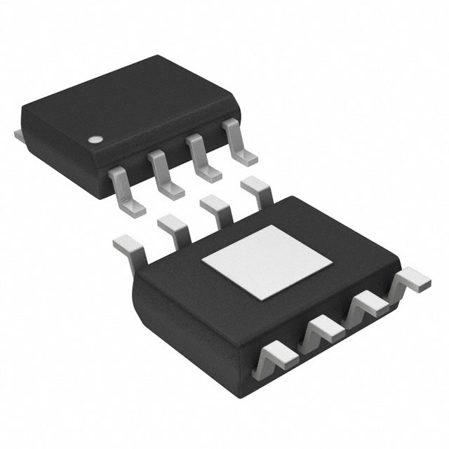
| 描述 | IC LED DRIVER 100MA 8-SOICLED照明驱动器 High-Voltage Linear w/LED Open Detect |
| 产品分类 | |
| 品牌 | Maxim Integrated |
| 产品手册 | |
| 产品图片 |
|
| rohs | 符合RoHS无铅 / 符合限制有害物质指令(RoHS)规范要求 |
| 产品系列 | LED照明电子器件,LED照明驱动器,Maxim Integrated MAX16839ASA+- |
| 数据手册 | |
| 产品型号 | MAX16839ASA+ |
| 产品培训模块 | http://www.digikey.cn/PTM/IndividualPTM.page?site=cn&lang=zhs&ptm=25703http://www.digikey.cn/PTM/IndividualPTM.page?site=cn&lang=zhs&ptm=25705 |
| 产品种类 | LED照明驱动器 |
| 供应商器件封装 | 8-SOIC N 裸露焊盘 |
| 其它有关文件 | |
| 内部驱动器 | 是 |
| 包装 | 管件 |
| 商标 | Maxim Integrated |
| 安装类型 | 表面贴装 |
| 安装风格 | SMD/SMT |
| 封装 | Tube |
| 封装/外壳 | 8-SOIC(0.154",3.90mm 宽)裸焊盘 |
| 封装/箱体 | SO-EP-8 |
| 工作温度 | -40°C ~ 125°C |
| 工厂包装数量 | 100 |
| 恒压 | - |
| 恒流 | 是 |
| 拓扑 | 线性,开路漏极,PWM |
| 最大工作温度 | + 125 C |
| 最大电源电流 | 15 mA to 100 mA |
| 最小工作温度 | - 40 C |
| 标准包装 | 1 |
| 电压-电源 | 5 V ~ 40 V |
| 电压-输出 | - |
| 类型-初级 | 车载 |
| 类型-次级 | 高亮度 LED(HBLED) |
| 系列 | MAX16839 |
| 输入电压 | 5 V to 40 V |
| 输出数 | 1 |
| 零件号别名 | MAX16839 |
| 频率 | - |


- 商务部:美国ITC正式对集成电路等产品启动337调查
- 曝三星4nm工艺存在良率问题 高通将骁龙8 Gen1或转产台积电
- 太阳诱电将投资9.5亿元在常州建新厂生产MLCC 预计2023年完工
- 英特尔发布欧洲新工厂建设计划 深化IDM 2.0 战略
- 台积电先进制程称霸业界 有大客户加持明年业绩稳了
- 达到5530亿美元!SIA预计今年全球半导体销售额将创下新高
- 英特尔拟将自动驾驶子公司Mobileye上市 估值或超500亿美元
- 三星加码芯片和SET,合并消费电子和移动部门,撤换高东真等 CEO
- 三星电子宣布重大人事变动 还合并消费电子和移动部门
- 海关总署:前11个月进口集成电路产品价值2.52万亿元 增长14.8%


PDF Datasheet 数据手册内容提取
19-4746; Rev 4; 4/11 EVAALVUAAILTAIOBNL EKIT High-Voltage, Linear High-Brightness LED Driver with Open-LED Fault Detect M General Description Features The MAX16839 programmable current regulator operates S 5V to 40V Operating Range A from a 5V to 40V input voltage range and features an S Integrated 2I Open-Drain Pass Transistor X open-drain, constant-current-sink output capable of sink- S 15mA to 100mA Programmable LED Current 1 ing up to 100mA. The MAX16839 is well suited for auto- 6 motive applications and other applications that require a S PWM Dimming 8 general-purpose linear LED driver. The device directly S Open-LED Fault Detection withstands automotive load-dump events of up to 45V. 3 S Open-LED Fault Event Status Memory 9 An on-board pass element minimizes external compo- S LED Open-Fault Detect Latches Off Multiple LED nent count while providing Q5% output current accuracy. Strings The MAX16839 includes a dimming input that controls S Multichip Synchronized LED Current Sink the duty cycle of the output current, allowing a wide LED dimming range. In addition, the dimming input functions S ±5% LED Current Accuracy as an on/off control of the output current. In multiple LED- S -40NC to +125NC Operating Temperature Range string applications, the dimming input synchronizes the S Thermal Protection LED current-sink turn-on, ensuring simultaneous bright- S Undervoltage Lockout ness in LED strings. S 6-Pin TDFN-EP and 8-Pin SO-EP Packages Additional features include thermal and open-LED protection and an open-LED fault-detection output. In Ordering Information multiple LED string applications where all FLTS pins are PART TEMP RANGE PIN-PACKAGE connected together, an open-LED detection in one LED string turns off all the strings simultaneously. Open-LED MAX16839ATT+ -40NC to +125NC 6 TDFN-EP* protection also features fault memory, to avoid LED flash- MAX16839ASA+ -40NC to +125NC 8 SO-EP* ing during subsequent power-up cycles. MAX16839ATT/V+ -40NC to +125NC 6 TDFN-EP* The MAX16839 is available in thermally enhanced, 6–pin +Denotes a lead(Pb)-free/RoHS-compliant package. TDFN-EP and 8-pin SO-EP packages and is specified *EP = Exposed pad. over the -40NC to +125NC automotive temperature range. /V denotes an automotive qualified part. Applications Typical Application Circuit Automotive Exterior: Turn Signal Light, Brake Light, Tail and Marker Lights VBAT VIN = 5V TO 40V Automotive Interior: Cluster and Warning Lights, Dome and Map Lights Truck, Train, Airplane, and Emergency Car LED REVERSE Lighting PROTECTION DIODE General Lighting: Signage, LED Lamps ILED = 100mA CIN = 0.01FF LEDs IN DIM SINK Pin Configurations appear at end of data sheet. MAX16839 FLTS CS CFLTS = 0.1FF GND RCS = 2I _______________________________________________________________ Maxim Integrated Products 1 For pricing, delivery, and ordering information, please contact Maxim Direct at 1-888-629-4642, or visit Maxim’s website at www.maxim-ic.com.
High-Voltage, Linear High-Brightness LED Driver with Open-LED Fault Detect 9 ABSOLUTE MAXIMUM RATINGS 3 (Voltages are specified with respect to GND.) Operating Temperature Range ........................-40NC to +125NC 8 IN, SINK .................................................................-0.3V to +45V Junction Temperature .....................................................+150NC 6 FLTS ......................................................................-0.3V to +18V Storage Temperature Range ............................-65NC to +150NC DIM ..........................................................................-0.3V to +6V Lead Temperature (soldering, 10s) ................................+300NC 1 CS .........................................................................-0.3V to +0.5V Soldering Temperature (reflow) ......................................+260NC X Continuous Current into SINK and CS .............................120mA A Continuous Power Dissipation (TA = +70NC) 6-Pin TDFN (derate 23.8mW/NC above +70NC) .....1904.8mW M 8-Pin SO (derate 18.9mW/NC above +70NC) ..........1509.4mW Stresses beyond those listed under “Absolute Maximum Ratings” may cause permanent damage to the device. These are stress ratings only, and functional operation of the device at these or any other conditions beyond those indicated in the operational sections of the specifications is not implied. Exposure to absolute maximum rating conditions for extended periods may affect device reliability. PACKAGE THERMAL CHARACTERISTICS (Note 1) TDFN SO Junction-to-Ambient Thermal Resistance (BJA) ..........42NC/W Junction-to-Ambient Thermal Resistance (BJA) ..........53NC/W Junction-to-Case Thermal Resistance (BJC) .....................9NC/W Junction-to-Case Thermal Resistance (BJC) .................5NC/W Note 1: Package thermal resistances were obtained using the method described in JEDEC specification JESD51-7, using a four-layer board. For detailed information on package thermal considerations, refer to www.maxim-ic.com/thermal-tutorial. ELECTRICAL CHARACTERISTICS (VIN = 12V, VFLTS = 0V, RCS = 4.07I, VGND = 0V, DIM = unconnected, CIN = 0.1FF (Note 2), TJ = TA = -40NC to +125NC, unless otherwise noted. Typical values are at TA = +25NC.) (Note 3) PARAMETER SYMBOL CONDITIONS MIN TYP MAX UNITS Supply Voltage Range VIN 5 40 V Quiescent Current IIN 0.25 0.6 mA Undervoltage Lockout VUVLO VIN rising 3.6 V UVLO Hysteresis 0.3 V CS REGULATOR TA = +25NC 195.5 203 210.5 CS Voltage Accuracy VCS -40NC P TA P +125NC, 0.9V P VSINK P 5.5V mV 193 213 (Note 4) CS Load Regulation 20mA P ISINK P 100mA 40 FV/mA Internal Switch On-Resistance RDS_ON (Note 5) 2 4 I LED CURRENT TRANSIENT RESPONSE 30% of VIN rising edge to 50% of ISINK, LED Current Turn-On Delay tDIN 4 9 Fs VDIM = 2.1V (Notes 6, 7) LED Current Turn-On Delay tDDIN VDIM rising edge to 50% of ISINK 2.3 5.5 Fs Relative to DIM LED Current Turn-Off Delay VDIM falling edge to 50% of ISINK 1.3 3.5 Fs Relative to DIM LED Current Rise Time tr 10% of ISINK to 90% of ISINK 2.5 5.5 Fs LED Current Fall Time tf 90% of ISINK to 10% of ISINK 2.5 6 Fs 2 ______________________________________________________________________________________
High-Voltage, Linear High-Brightness LED Driver with Open-LED Fault Detect ELECTRICAL CHARACTERISTICS (continued) M (VIN = 12V, VFLTS = 0V, RCS = 4.07I, VGND = 0V, DIM = unconnected, CIN = 0.1FF (Note 2), TJ = TA = -40NC to +125NC, unless A otherwise noted. Typical values are at TA = +25NC.) (Note 3) X PARAMETER SYMBOL CONDITIONS MIN TYP MAX UNITS 1 FAULT EVENT STATUS MEMORY 6 FLTS Activation Threshold VINTH VIN rising, VCS = 0V 7 7.38 7.75 V 8 FLTS Activation Hysteresis 20 mV 3 LED Open Threshold VCSO 25 30 35 mV 9 LED Open Blanking TB 14 25 50 Fs Fault Voltage VFLTS VIN = 40V, VCS = 0V, CFLTS = 0.1FF 12 15 18 V FLTS Charge Current ICFLTS VCS P 25mV 0.65 2.8 4.8 mA FLTS Discharge Current VFLTS = 0.5V 2.25 5 7.25 FA FLTS Threshold To Turn Off LED VFLTH 0.95 1.3 1.65 V Current Sink DIM LOGIC Input High Voltage VIH 2.1 V Input Low Voltage VIL 0.8 V DIM Voltage Logic Hysteresis VDIM_HYS 0.15 V DIM Pullup Current VDIM = 0V 10 30 60 FA DIM Pulldown Current VDIM = 0.8V, VIN = 2.4V 0.385 1 1.5 mA DIM Pulse Width 70 Fs DIM Frequency fDIM 10 kHz LEAKAGE CURRENTS SINK Leakage Current VSINK = 40V, VDIM = 0V 1 FA FLTS Leakage Current VFLTS = 8V, VIN = 0V 1 FA THERMAL SHUTDOWN Thermal Shutdown Temperature Temperature rising 160 NC Thermal Shutdown Hysteresis 15 NC Note 2: A 51I resistor is connected between SINK and a 6.5V supply to reduce power dissipation during the factory test. Note 3: All devices are 100% production tested at TA = +25NC. Limits over temperature are guaranteed by design. Note 4: Guaranteed by design and not production tested. Note 5: Internal switch resistance is measured with ISINK = 0.95 x ISINK0 (ISINK0 is ISINK at VSINK = 0.9V). Note 6: Supply turn-on delay will be measured by rising supply in 6Fs from GND to 12V, and measurement starts when VIN = 4V (typical UVLO). Note 7: DIM is kept high to avoid delay due to high capacitance from test setup. In applications, a 30FA pullup current charges parasitic capacitance at DIM with negligible delay. Ensure that unnecessary capacitance is not added at DIM during the PCB layout. _______________________________________________________________________________________ 3
High-Voltage, Linear High-Brightness LED Driver with Open-LED Fault Detect 9 Typical Operating Characteristics 3 (VIN = 12V, RCS = 4.07I from CS to GND, CFLTS = 0.1FF, CIN = 0.1FF, DIM input unconnected, TA = +25NC, unless otherwise noted. 8 Typical values are at TA = +25NC.) 6 1 OUTPUT CURRENT vs. TEMPERATURE OUTPUT CURRENT vs. TEMPERATURE OUTPUT CURRENT vs. TEMPERATURE AX 111667...890 ILOAD = 16mA MAX16839 toc01a 445990...890 ILOAD = 50mA MAX16839 toc01b 999889...680 ILOAD = 100mA MAX16839 toc01c M mA) 16.7 mA) 49.7 mA) 98.4 URRENT ( 1166..56 URRENT ( 4499..56 URRENT ( 9988..02 C C C UT 16.4 UT 49.4 UT 97.8 OUTP 16.3 OUTP 49.3 OUTP 97.6 16.2 49.2 97.4 16.1 49.1 97.2 16.0 49.0 97.0 -40-25-10 5 20 35 50 65 80 95 110125 -40-25-10 5 20 35 50 65 80 95 110125 -40-25-10 5 20 35 50 65 80 95 110125 TEMPERATURE (NC) TEMPERATURE (NC) TEMPERATURE (NC) VCS vs. OUTPUT CURRENT OUTPUT CURRENT vs. INPUT VOLTAGE RDS(ON) VS. TEMPERATURE 222000445...050 VIN = 12V MAX16839 toc02 110200 IILED = 100mA MAX16839 toc03 223...680 VIN = 12V MAX16839 toc04 203.5 mA) 2.4 V (mV)CS222000223...050 UT CURRENT ( 6800 IILED = 50mA IR ()DS(ON) 122...802 P 201.5 OUT 40 1.6 201.0 20 IILED = 15mA 1.4 200.5 1.2 200.0 0 1.0 10 20 30 40 50 60 70 80 90 100 5 10 15 20 25 30 35 40 -40-25-10 5 20 35 50 65 80 95 110125 OUTPUT CURRENT (mA) VIN (V) TEMPERATURE (NC) QUIESCENT CURRENT vs. TEMPERATURE LED CURRENT RISE TIME LED CURRENT FALL TIME 400 MAX16839 toc06 MAX16839 toc07 A) 335705 VIN = 12V MAX16839 toc05 VDIM VDIM F 2V/div 2V/div T ( EN 325 0V 0V R R U C 300 T N ESCE 275 LED CURRENT LED CURRENT UI 50mA/div Q 250 50mA/div 225 0 0 200 -40-25-10 5 20 35 50 65 80 95 110125 2Fs/div 2Fs/div TEMPERATURE (NC) 4 ______________________________________________________________________________________
High-Voltage, Linear High-Brightness LED Driver with Open-LED Fault Detect Typical Operating Characteristics (continued) M (VIN = 12V, RCS = 4.07I from CS to GND, CFLTS = 0.1FF, CIN = 0.1FF, DIM input unconnected, TA = +25NC, unless otherwise noted. A Typical values are at TA = +25NC.) X LED CURRENT RISE/FALL TIMES FLTS DISCHARGE LEAKAGE CURRENT vs. TEMPERATURE 1 MAX16839 toc08 V2VD/IMdiv VIN IS TURNMEAXD16 O83F9 Ftoc09 V5VIN/div 4500 VVIFNL T=S 0 =V 8V MAX16839 toc10 683 A) n 0V 0V NT ( 30 9 E R R CU 20 E G I5L0EmDA/div V5VFL/dTSiv LEAKA 10 0 0 0V -10 20Fs/div 1s/div -40-25-10 5 20 35 50 65 80 95 110125 TEMPERATURE (NC) FAULT ACTIVATION THRESHOLD vs. TEMPERATURE ILED RESPONSE TO SUPPLY CHOPPING 7.40 MAX16839 toc12 D (V) 77..3389 MAX16839 toc11 L HO 7.37 VIN S E 5V/div HR 7.36 T ON 7.35 TI VA 7.34 CTI ILED T A 7.33 20mA/div L AU 7.32 F 0 7.31 7.30 -40-25-10 5 20 35 50 65 80 95 110125 4ms/div TEMPERATURE (NC) LED RISE TIME DELAY FAULT ACTIVATION THRESHOLD (SUPPLY CHOPPING) AND OPEN-LED BLANKING MAX16839 toc13 MAX16839 toc14 VIN VIN 5V/div 2V/div 0V I2L0EmDA/div VFLTS 2V/div 0 0V 1Fs/div 20Fs/div _______________________________________________________________________________________ 5
High-Voltage, Linear High-Brightness LED Driver with Open-LED Fault Detect 9 Typical Operating Characteristics (continued) 3 (VIN = 12V, RCS = 4.07I from CS to GND, CFLTS = 0.1FF, CIN = 0.1FF, DIM input unconnected, TA = +25NC, unless otherwise noted. 8 Typical values are at TA = +25NC.) 6 1 FAULT INTEGRATION ON OPEN LED FAULT INTEGRATION ON OPEN LED FAULT INTEGRATION ON OPEN LED X (100Hz, 50% DUTY CYCLE AT DIM) (100Hz, 75% DUTY CYCLE AT DIM) WITH SUPPLY CHOPPING MAX16839 toc15a MAX16839 toc15b MAX16839 toc16 A 100Hz AT DIM M VCS VFLT 5V/div VFLT 5V/div 200mV/div VIN VDIM 2V/div VDIM 2V/div 5V/div VFLTS 5V/div ILED 500mA/div ILED 500mA/div 4ms/div 100µs/div 200Fs/div Pin Description PIN NAME FUNCTION TDFN SO 1 1 IN Positive Input Supply. Bypass with a 10nF (typ) capacitor to GND. Dimming Input. Drive DIM high or leave unconnected to turn on the LED current-sink driver. 2 2 DIM Drive DIM low to turn off the LED current-sink driver. In multiple LED-string applications, connect all DIM inputs together to synchronize the LED current-sink turn-on. LED Fault Memory. Connect a 0.1FF to 10FF capacitor from FLTS to ground. In multiple LED- 3 3 FLTS string applications, connect all FLTS pins together to have all strings latch off if one of them opens (see Figure 2). Connect FLTS to ground to disable fault protection. 4 6 GND Ground Current-Sense Input. Connect a current-sense resistor between CS and GND to program the 5 7 CS output current level. 6 8 SINK LED Driver Current-Sink Output — 4, 5 N.C. No Connection. Not internally connected. Exposed Pad. Connect EP to a large-area contiguous copper ground plane for effective power — — EP dissipation. Do not use as the only IC ground connection. EP must be connected to GND. 6 ______________________________________________________________________________________
High-Voltage, Linear High-Brightness LED Driver with Open-LED Fault Detect Detailed Description Additional features include thermal protection and an M open-LED detection output that can turn off multiple LED The MAX16839 programmable current regulator oper- A strings simultaneously. See Figure 1. ates from a 5V to 40V input voltage range and features X an open-drain, constant-current-sink output capable of Open-LED Detection and 1 sinking up to 100mA. The MAX16839 directly withstands Fault Event Status Memory 6 automotive load-dump events of up to 45V. The MAX16839 has an integrated open-LED detection that reduces external components required to implement 8 A single resistor-programmable output current and on- this function. The following conditions enable the open- 3 board pass element minimize the number of external LED detection feature: 9 components while providing Q5% output current accuracy. The MAX16839 includes a dimming input that controls U FLTS not connected to ground the duty cycle of the output current, allowing a wide U VIN > VINTH (7.38V) (typ) LED dimming range to be implemented. In addition, the U Thermal shutdown inactive dimming input functions as an on/off control of the output current. In multiple LED-string applications, the U VDIM = High dimming input synchronizes the LED current-sink turn-on, ensuring simultaneous brightness in LED strings. IN 5V REG SINK 5V IREG 30µA REFERENCE GENERATOR CS DIM IN 15V CLAMP MAX16839 1mA ENABLE 2.8mA 1.65V OPEN-LED DETECT THERMAL FLTS SHDN FAULT GND Figure 1. Internal Block Diagram _______________________________________________________________________________________ 7
High-Voltage, Linear High-Brightness LED Driver with Open-LED Fault Detect 9 The MAX16839 detects an open-LED event when VCS used. If the retention capability is high, the fault condition 3 drops below 30mV for 25µs. When the fault condition is could be retained or memorized for a long period after the 8 detected, a 2.8mA current source charges the capaci- supply is turned off. 6 tor between FLTS and ground, up to 15V or to VIN if VIN Thermal Protection is less than 15V. If the voltage on FLTS is greater than 1 The MAX16839 enters thermal-shutdown mode in the 1.65V due to the charge retained in the FLTS capacitor, X event of overheating. When the junction temperature the LED driver is turned off. This provides an open-LED A fault-protection feature that can be disabled by connect- exceeds TJ = +160NC, the internal thermal-protection circuit turns off the series pass element. The MAX16839 M ing FLTS to ground. In a multistring application (Figure recovers from thermal-shutdown mode when the 2), where all FLTS pins are connected together, a fault detected on one channel causes other channels to turn junction temperature drops to TJ = +145NC. FLTS does not assert during an overheating event. off as well. The retention capability on the FLTS is depen- dent on the leakage current and the value of the capacitor VIN VIN 12V 12V t UVLO ILED 50mA t t LEDGOOD (INTERNAL) ILED 50mA t 12V FLTS t t 2.5Fs 4Fs VIN = 5V TO 40V LEDS 0.0C1INF =F SCUOPNPNLYE COTR T LOE A5VVE C0.I0N1 =FF LEDS UNCONNECTED IN DIM SIGNAL IN ILED ILED SINK DIM DIM SINK MAX16839 MAX16839 FLTS SIGNAL CS FLTS FLTS CS GND GND RCS CFLTS = RCS 0.1FF Figure 2. Multistring Application 8 ______________________________________________________________________________________
High-Voltage, Linear High-Brightness LED Driver with Open-LED Fault Detect Applications Information dropout voltage of the regulator. If the device is oper- M ated below VIN(MIN), the output current may not meet the A FLTS Capacitor full regulation specification (see the Typical Operating If a fault condition is detected, a 2.8mA current source Characteristics). X charges CFLTS to memorize the fault condition and avoid For applications that require more than 3 LEDs per string 1 flashing during the subsequent power-up cycles. The and have slow supply rise time (> 14Fs), FLTS should, in 6 choice of the CFLTS is based on the following conditions: general, be connected to ground to avoid false trigger- 8 U Fault hold time ing of the open-LED protection. 3 U Board leakage and FLTS leakage 9 PWM Dimming U Input supply voltage, as this affects the maximum The MAX16839 includes a PWM dimming input (DIM) FLTS voltage to control the LED brightness. An application of up to a U The number of ICs connected together in case of a 10kHz signal is recommended at DIM for proper opera- multistring application tion. DIM also functions as an active-high enable input. Driving DIM low turns off the output. Driving DIM high or Use the following equation to calculate the FLTS capaci- leaving DIM unconnected turns on the output. tor (CFLTS): For VIN > undervoltage-lockout threshold, the MAX16839 I ×t ×N activates a 30FA (typ) pullup current at DIM. When VIN < CFLTS = FLTS FLTS undervoltage-lockout threshold, the MAX16839 activates (V −V ) FLTS FLTH a 1mA pulldown current. where IFLTS is the maximum leakage current through Supply Chopped Dimming FLTS, tFLTS is the desired fault retention period, VFLTS The MAX16839 can do efficient supply chopped is the typical voltage (minimum of 15V or the supply dimming, as it is specially designed for very low startup voltage) to which CFLTS is charged during a fault event, delay. The LED current is turned on in 4Fs (typ) after VFLTH is the minimum threshold to detect the fault the supply comes up. The LED current pulse-width memory as logic-high, and N is the number of devices in modulates in phase with the supply voltage. Minimize the a multistring application. input filter capacitor after the chopper circuit for fast rise and fall times of the input supply. Programming the LED Current The MAX16839 uses a sense resistor to program the Power Dissipation output current sink. To program the LED current, connect The power dissipation (PD) of the MAX16839 is a sense resistor from the current-sense input (CS) to determined from the following equation: GND with short traces. The value of the sense resistor for a given desired current is calculated with the follow- PD =(VIN×IIN)+(VIN−∑VLED−VCS)×(ILED×DUTY) ing equation: where: R (Ω)= VCS(V) VIN = Supply voltage CS I (A) LED IIN = Supply current where VCS is 203mV (typ) (see the Electrical CVLED = Total forward voltage for the LED string Characteristics table). ILED = LED current Input Voltage VCS = 203mV drop across RCS For proper operation, the minimum input voltage must DUTY = PWM duty cycle always be: The MAX16839 thermal specifications are given accord- ing to the JEDEC-51 guidelines. Good mechanical/ V =V +V +∆V IN(MIN) CS(MAX) FT(MAX) DO thermal design practices must be applied to help maintain the device junction temperature below the where VCS(MAX) is the maximum voltage drop across the absolute maximum ratings at all times. sense resistor RCS, VFT(MAX) is the total forward voltage of all series-connected LEDs, and DVDO is the maximum _______________________________________________________________________________________ 9
High-Voltage, Linear High-Brightness LED Driver with Open-LED Fault Detect 9 Pin Configurations 3 8 6 TOP VIEW 1 X A + + IN 1 8 SINK M IN 1 6 SINK DIM 2 7 CS DIM 2 5 CS MAX16839 MAX16839 FLTS 3 6 GND EP FLTS 3 4 GND EP N.C. 4 5 N.C. TDFN SO Chip Information Package Information PROCESS: BiCMOS DMOS For the latest package outline information and land patterns (footprints), go to www.maxim-ic.com/packages. Note that a “+”, “#”, or “-” in the package code indicates RoHS status only. Package drawings may show a different suffix character, but the drawing pertains to the package regardless of RoHS status. PACKAGE PACKAGE OUTLINE LAND TYPE CODE NO. PATTERN NO. 6 TDFN-EP T633+2 21-0137 90-0058 8 SO-EP S8E+12 21-0111 90-0150 10 _____________________________________________________________________________________
High-Voltage, Linear High-Brightness LED Driver with Open-LED Fault Detect Revision History M A REVISION REVISION PAGES DESCRIPTION X NUMBER DATE CHANGED 0 7/9 Initial release — 1 6 1 5/10 Changed one feature of IC; replaced TOC 15 with two TOCs 1, 2, 3, 5–11 8 2 12/10 Corrected fault description 7, 8, 10 3 3 1/11 Corrected block diagram 7 9 4 4/11 Added automotive part 1, 2 Maxim cannot assume responsibility for use of any circuitry other than circuitry entirely embodied in a Maxim product. No circuit patent licenses are implied. Maxim reserves the right to change the circuitry and specifications without notice at any time. Maxim Integrated Products, 120 San Gabriel Drive, Sunnyvale, CA 94086 408-737-7600 11 © 2011 Maxim Integrated Products Maxim is a registered trademark of Maxim Integrated Products, Inc.