ICGOO在线商城 > 集成电路(IC) > PMIC - LED 驱动器 > TPS61199PWPR
 Datasheet下载
- 型号: TPS61199PWPR
- 制造商: Texas Instruments
- 库位|库存: xxxx|xxxx
- 要求:
| 数量阶梯 | 香港交货 | 国内含税 |
| +xxxx | $xxxx | ¥xxxx |
查看当月历史价格
查看今年历史价格
TPS61199PWPR产品简介:
ICGOO电子元器件商城为您提供TPS61199PWPR由Texas Instruments设计生产,在icgoo商城现货销售,并且可以通过原厂、代理商等渠道进行代购。 TPS61199PWPR价格参考。Texas InstrumentsTPS61199PWPR封装/规格:PMIC - LED 驱动器, LED 驱动器 IC 8 输出 DC DC 控制器 升压 PWM 调光 70mA 20-HTSSOP。您可以下载TPS61199PWPR参考资料、Datasheet数据手册功能说明书,资料中有TPS61199PWPR 详细功能的应用电路图电压和使用方法及教程。
TPS61199PWPR 是 Texas Instruments(德州仪器)生产的一款 PMIC(电源管理集成电路),具体分类为 LED 驱动器。它主要应用于需要高效、稳定驱动 LED 的电子设备中。

该器件是一款升压型 DC-DC 转换器,内置 40V/1.2A 开关,能够将较低的输入电压升压以驱动多个串联或并联的 LED。其高集成度和灵活的调光功能使其适用于多种照明应用场景。

典型的应用场景包括:

1. 背光照明:用于 LCD 显示屏的 LED 背光驱动,如平板电脑、笔记本电脑、工业显示屏等;
2. 手持设备照明:如智能手机、便携式医疗设备中的 LED 灯或闪光灯;
3. 通用LED照明:适用于需要恒流驱动的小功率至中功率 LED 照明系统;
4. 汽车照明:可用于车内照明或辅助灯具的 LED 驱动;
5. 工业与消费类电子产品:如条形灯、指示灯、装饰灯等对亮度控制有需求的应用。

该芯片支持 PWM 调光和模拟调光方式,具备过压保护、过流保护和热关断等功能,提高了系统的可靠性和安全性。
| 参数 | 数值 |
| 产品目录 | 集成电路 (IC)光电子产品 |
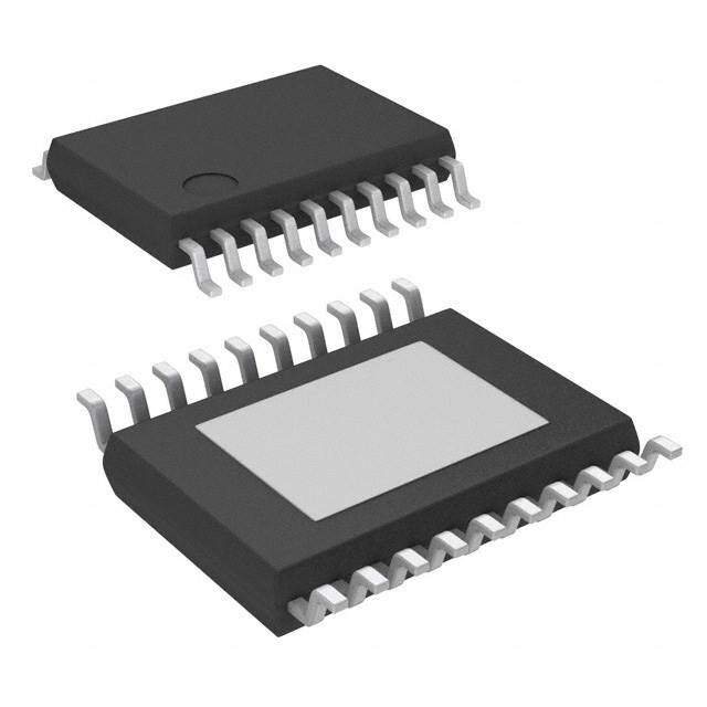
| 描述 | IC LED DVR WHITE BCKLGT 20HTSSOPLED照明驱动器 White LED Driver |
| 产品分类 | |
| 品牌 | Texas Instruments |
| 产品手册 | |
| 产品图片 |
|
| rohs | 符合RoHS无铅 / 符合限制有害物质指令(RoHS)规范要求 |
| 产品系列 | LED照明电子器件,LED照明驱动器,Texas Instruments TPS61199PWPR- |
| 数据手册 | |
| 产品型号 | TPS61199PWPR |
| PCN设计/规格 | |
| 产品种类 | LED照明驱动器 |
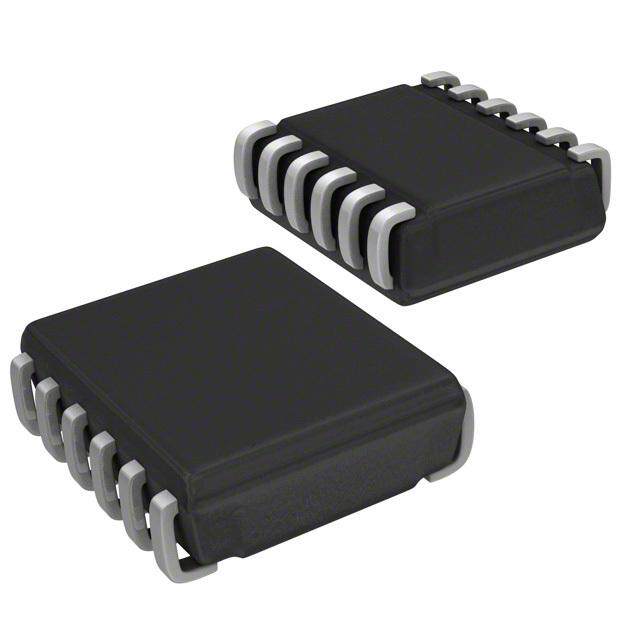
| 供应商器件封装 | 20-HTSSOP |
| 其它名称 | 296-28161-1 |
| 内部驱动器 | 无 |
| 包装 | 剪切带 (CT) |
| 商标 | Texas Instruments |
| 安装类型 | 表面贴装 |
| 安装风格 | SMD/SMT |
| 封装 | Reel |
| 封装/外壳 | 20-TSSOP(0.173",4.40mm 宽)裸焊盘 |
| 封装/箱体 | HTSSOP-20 |
| 工作温度 | -40°C ~ 85°C |
| 工作频率 | 300 kHz to 800 kHz |
| 工厂包装数量 | 2000 |
| 恒压 | - |
| 恒流 | - |
| 拓扑 | PWM,升压(升压) |
| 拓扑结构 | Boost |
| 最大工作温度 | + 85 C |
| 最大电源电流 | 1.5 mA |
| 最小工作温度 | - 40 C |
| 标准包装 | 1 |
| 电压-电源 | 8 V ~ 30 V |
| 电压-输出 | - |
| 类型 | Inductive |
| 类型-初级 | 背光,通用 |
| 类型-次级 | 白色 LED |
| 系列 | TPS61199 |
| 输入电压 | 8 V to 30 V |
| 输出数 | 8 |
| 输出电流 | 70 mA |
| 输出端数量 | 8 Output |
| 输出类型 | Current Mode |
| 频率 | 500kHz ~ 800kHz |


- 商务部:美国ITC正式对集成电路等产品启动337调查
- 曝三星4nm工艺存在良率问题 高通将骁龙8 Gen1或转产台积电
- 太阳诱电将投资9.5亿元在常州建新厂生产MLCC 预计2023年完工
- 英特尔发布欧洲新工厂建设计划 深化IDM 2.0 战略
- 台积电先进制程称霸业界 有大客户加持明年业绩稳了
- 达到5530亿美元!SIA预计今年全球半导体销售额将创下新高
- 英特尔拟将自动驾驶子公司Mobileye上市 估值或超500亿美元
- 三星加码芯片和SET,合并消费电子和移动部门,撤换高东真等 CEO
- 三星电子宣布重大人事变动 还合并消费电子和移动部门
- 海关总署:前11个月进口集成电路产品价值2.52万亿元 增长14.8%


PDF Datasheet 数据手册内容提取
Product Sample & Technical Tools & Support & Folder Buy Documents Software Community TPS61199 SLVSAN3B–DECEMBER2010–REVISEDNOVEMBER2016 TPS61199 White-LED Driver for LCD Monitor Backlighting 1 Features 3 Description • 8-Vto30-VInputVoltage The TPS61199 provides highly integrated solutions 1 forlargesizeLCDbacklighting.Thisdeviceintegrates • IntegratedHigh-PowerBoostController a current-mode boost controller and eight current • AdaptiveBoostOutputforLEDVoltages sinks for driving up to eight LED strings with multiple • DriveuptoEightLEDStringsinParallel LEDs in series. Each string has an independent current regulator with current matching between • Maximum70mAforEachLEDString strings reaching 3% regulation accuracy. The device • 3%CurrentMatchingBetweenStrings automatically adjusts the output voltage of the boost • 5000:1PWMDimmingRatioat200Hz converter to provide only the voltage required by the LED string with the largest forward voltage drop plus • MOSFETOvercurrentProtection the minimum required voltage at the IFBx pin of that • ProgrammableLEDShortProtection string,therebyoptimizingefficiencyofthedriver. • AdjustableLEDOpenProtection The TPS61199 provides PWM brightness dimming • ThermalShutdownProtection with an external PWM signal. The signal of the PWM • 20-PinSOPackageandTSSOPPackage maximum frequency can be as high as 22 kHz. WithPowerPAD™ Dimming ratios up to 5000:1 can be achieved with a 200-Hz PWM signal. The TPS61199 integrates 2 Applications overcurrent protection for the switch FET, soft start- up, LED short protection, LED open protection, and • MonitorLCDBacklight overtemperature shutdown protection. The TPS61199 • LCDTVBacklight device is available in 20-pin SO and HTSSOP • GeneralLEDLighting packages. DeviceInformation(1) PARTNUMBER PACKAGE BODYSIZE(NOM) SO(20) 12.60mm×5.30mm TPS61199 HTSSOP(20) 6.50mm×4.40mm (1) For all available packages, see the orderable addendum at theendofthedatasheet. TypicalApplication 12V IN L1 D1 OUT 60V 22µH SS5P10 C1 + 10µF R8 C2 3Ω Q1 3 X 33µF Si4480DY R9 200Ω C3 OUT 2.2µF VIN GDRV C6 R1 VDD ISNS 0.47nF 0.03Ω R1920kΩ GND IFB1 IFB2 OVP IFB3 TPS61199 10kΩ R3 IFB4 EN 10kΩ IFB5 10kΩ PWM IFB6 IFB7 COMP IFB8 FBP R504kΩ ISET FSW R2050kΩ C0.547nF R6 R7 C4 40.2kΩ 160kΩ 47nF Copyright©2016,TexasInstrumentsIncorporated 1 An IMPORTANT NOTICE at the end of this data sheet addresses availability, warranty, changes, use in safety-critical applications, intellectualpropertymattersandotherimportantdisclaimers.PRODUCTIONDATA.
TPS61199 SLVSAN3B–DECEMBER2010–REVISEDNOVEMBER2016 www.ti.com Table of Contents 1 Features.................................................................. 1 8 ApplicationandImplementation........................ 12 2 Applications........................................................... 1 8.1 ApplicationInformation............................................12 3 Description............................................................. 1 8.2 TypicalApplication .................................................12 4 RevisionHistory..................................................... 2 9 PowerSupplyRecommendations...................... 17 5 PinConfigurationandFunctions......................... 3 10 Layout................................................................... 17 6 Specifications......................................................... 4 10.1 LayoutConsideration............................................17 6.1 AbsoluteMaximumRatings.....................................4 10.2 LayoutExample....................................................17 6.2 ESDRatings..............................................................4 11 DeviceandDocumentationSupport................. 18 6.3 RecommendedOperatingConditions......................4 11.1 DeviceSupport ....................................................18 6.4 ThermalInformation..................................................4 11.2 RelatedDocumentation .......................................18 6.5 ElectricalCharacteristics..........................................5 11.3 ReceivingNotificationofDocumentationUpdates18 6.6 TypicalCharacteristics..............................................6 11.4 CommunityResources..........................................18 7 DetailedDescription.............................................. 8 11.5 Trademarks...........................................................18 7.1 Overview...................................................................8 11.6 ElectrostaticDischargeCaution............................18 7.2 FunctionalBlockDiagram.........................................8 11.7 Glossary................................................................18 7.3 FeatureDescription...................................................9 12 Mechanical,Packaging,andOrderable Information........................................................... 18 7.4 DeviceFunctionalModes........................................10 4 Revision History NOTE:Pagenumbersforpreviousrevisionsmaydifferfrompagenumbersinthecurrentversion. ChangesfromRevisionA(May2011)toRevisionB Page • AddedDeviceInformationandPinConfigurationandFunctionssections,ESDRatingstable,FeatureDescription, DeviceFunctionalModes,ApplicationandImplementation,PowerSupplyRecommendations,Layout,Deviceand DocumentationSupport,andMechanical,Packaging,andOrderableInformationsections;deleteDevice Comparisontable-infoinPOA.............................................................................................................................................. 1 ChangesfromOriginal(December2010)toRevisionA Page • ChangedtoRevA,May2011................................................................................................................................................ 1 • Changedfrom65mAto70mAinfifthlistItemofFeatures.................................................................................................. 1 • ChangedABSMAXtableMAXcolumn,row1to33andthe4throwto3.6......................................................................... 4 • ChangedElectricalCharacteristicstable,CurrentRegulation,I specMINvaluefrom65to70mA............................ 5 IFB_max • ChangedvaluesinELECCHARTABLE,OSCILLATORsection,first2rows0.66,0.8,0.94and0.44,0.5,0.56............... 5 • ChangedvaluesinELECCHARTABLE,PROTECTIONsection,firstrowtomin2.77,max3.13....................................... 5 • Addedaparagraph:Fs(inkHz)=80,000/R7(inkΩ).......................................................................................................... 9 • Changed65mAto70mAinparagraphinProgramLEDFull-ScaleCurrent...................................................................... 10 • Changed65mAto70mAinparagraphinDriveHighCurrentLED.................................................................................... 10 • AddedListItemnumber4toOrderedListunderProtectionsection..................................................................................... 10 • ChangedoraddedtheparagraphCurrentSenseandCurrentSenseFiltering................................................................... 14 2 SubmitDocumentationFeedback Copyright©2010–2016,TexasInstrumentsIncorporated ProductFolderLinks:TPS61199
TPS61199 www.ti.com SLVSAN3B–DECEMBER2010–REVISEDNOVEMBER2016 5 Pin Configuration and Functions NSPackage PWPPackage 20-PinSO 20-PinHTSSOP TopView TopView FBP 1 20 OVP FBP 1 20 OVP COMP 2 19 VDD COMP 2 19 VDD FSW 3 18 VIN FSW 3 18 VIN ISET 4 P 17 GDRV EN 5 o 16 ISNS ISET 4 17 GDRV PWM 6 werP 15 GND EN 5 16 ISNS IFB8 7 A 14 IFB1 D IFB7 8 13 IFB2 PWM 6 15 GND IFB6 9 12 IFB3 IFB8 7 14 IFB1 IFB5 10 11 IFB4 IFB7 8 13 IFB2 IFB6 9 12 IFB3 IFB5 10 11 IFB4 PinFunctions PIN TYPE DESCRIPTION NAME NO. Loopcompensationpin.ConnectanRCnetworktomakeloopstable(seeLoop COMP 2 Output Consideration). EN 5 Input Enable/disablepin—high=deviceisenabled;low=deviceisdisabled. FBP 1 Output LEDshort-acrossprotectionthresholdprogrampin(seeProtection) Boostswitchingfrequencyselectionpin.Connectaresistortosetthefrequency FSW 3 Output between300kHzto800kHz. GDRV 17 Output ExternalSwitchMOSFETgatedriveroutputpin GND 15 Ground Groundpin 7,8,9,10,11 IFB1toIFB8 Input Regulatedcurrentsinkinputpins. 12,13,14 Full-scaleLEDcurrentselectionpin;connectaresistortoprogramLEDcurrent ISET 4 Output foreachstring ISNS 16 Input ExternalMOSFETcurrentsensepositiveinputpin OVP 20 Input Overvoltageprotectionpin(seeProtection) PWMdimmingsignalinputpin.Thefrequencymustbeintherangeof100Hzto PWM 6 Input 22kHz. Internalregulatoroutputpin.Connecta2.2-μFcapacitorbetweenthispinto VDD 19 Output GND. Supplyinputpin.Thispincanbetiedtoavoltagedifferentfromthepowerstage VIN 18 Input input. ThePowerPADpadmustbesolderedtotheground.Ifpossible,usethermalvias PowerPAD–HTTSOPpackage — toconnecttotopandinternalgroundplanelayersforidealpowerdissipation. Copyright©2010–2016,TexasInstrumentsIncorporated SubmitDocumentationFeedback 3 ProductFolderLinks:TPS61199
TPS61199 SLVSAN3B–DECEMBER2010–REVISEDNOVEMBER2016 www.ti.com 6 Specifications 6.1 Absolute Maximum Ratings overoperatingfree-airtemperaturerange(unlessotherwisenoted)(1) MIN MAX UNIT PinVIN(2) –0.3 33 PinIFB1toIFB8(2) –0.3 30 Voltage PinENandPWM(2) –0.3 20 V PinISET,ISNSandOVP(2) –0.3 3.6 Allotherpins(2) –0.3 7 Continuouspowerdissipation SeeThermalInformation Operatingjunctiontemperature –40 150 °C Storagetemperature,T –65 50 °C stg (1) StressesbeyondthoselistedunderAbsoluteMaximumRatingsmaycausepermanentdamagetothedevice.Thesearestressratings only,whichdonotimplyfunctionaloperationofthedeviceattheseoranyotherconditionsbeyondthoseindicatedunderRecommended OperatingConditions.Exposuretoabsolute-maximum-ratedconditionsforextendedperiodsmayaffectdevicereliability. (2) Allvoltagevaluesarewithrespecttonetworkgroundterminal 6.2 ESD Ratings VALUE UNIT V Electrostaticdischarge Human-bodymodel(HBM),perANSI/ESDA/JEDECJS-001(1) ±2000 V (ESD) (1) JEDECdocumentJEP155statesthat500-VHBMallowssafemanufacturingwithastandardESDcontrolprocedures. 6.3 Recommended Operating Conditions overoperatingfree-airtemperaturerange(unlessotherwisenoted)(1) MIN NOM MAX UNIT Inductor,L1 10 22 47 µH Inputcapacitor,C1 10 µF Outputcapacitor,C2 10 33 100 µF PWMdimmingfrequency,ƒ 0.1 22 KHz PWM Rising/fallingedgeofPWMsignal,t 1 µsec PWM Boostregulatorswitchingfrequency,f 300 800 kHz BOOST Operatingambienttemperature,T –40 85 °C A (1) Customersmustverifythecomponentvaluesintheirapplicationifthevaluesaredifferentfromtherecommendedvalues. 6.4 Thermal Information TPS61199 TPS61199 THERMALMETRIC(1) NS(SO) PWP(HTSSOP) UNITS 20PINS 20PINS R Junction-to-ambientthermalresistance 69.4 46.9 °C/W θJA R Junction-to-case(top)thermalresistance 36.4 48.2 °C/W θJC(top) R Junction-to-boardthermalresistance 37.3 22.1 °C/W θJB ψ Junction-to-topcharacterizationparameter 11.0 3.4 °C/W JT ψ Junction-to-boardcharacterizationparameter 36.8 13.3 °C/W JB R Junction-to-case(bottom)thermalresistance n/a 2.3 °C/W θJC(bot) (1) Formoreinformationabouttraditionalandnewthermalmetrics,seeSemiconductorandICPackageThermalMetrics. 4 SubmitDocumentationFeedback Copyright©2010–2016,TexasInstrumentsIncorporated ProductFolderLinks:TPS61199
TPS61199 www.ti.com SLVSAN3B–DECEMBER2010–REVISEDNOVEMBER2016 6.5 Electrical Characteristics V =12V;T =–40°Cto+85°C,typicalvaluesareatT =25°C(unlessotherwisenoted) IN A A PARAMETER TESTCONDITIONS MIN TYP MAX UNIT SUPPLYCURRENT VIN Inputvoltagerange 8 30 V V Undervoltagelockoutthreshold V falling 6.5 7 V UVLO_VIN IN V VINhysteresis V rising 300 mV VIN_SYS IN Operatingquiescentcurrentinto EN=high;PWM=low; I 1.5 mA Q_VIN VIN noswitching,V =30V IN I Shutdowncurrent 10 µA SD VDD Internalregulationvoltage OutputcurrentofV =15mA 5.7 6 6.3 V DD ENandPWM V LogichighthresholdonEN,PWM V =8Vto30V 2 V H IN V LogiclowthresholdonEN,PWM V =8Vto30V 0.8 V L IN R PulldownresistoronEN,PWM 400 800 1600 kΩ PD CURRENTREGULATION V ISETpinvoltage 1.204 1.229 1.253 V ISET K CurrentmultipleI /I I =30µA;IFB=450mV 1990 ISET IFB(AVG) SET ISET IFB CurrentaccuracytoI I =30µA;IFB=450mV –2% 2% IFB(AVG) ISET IFB (1) Currentmatching I =30µA;IFB=450mV 3% (BR) ISET IFB IFBpinleakagecurrent IFBvoltage=30V;PWM=low 10 25 45 µA leak I Currentsinkmaxoutputcurrent IFB=450mV 70 mA IFB_max OSCILLATOR R=100kΩ 0.66 0.8 0.94 ƒ Switchingfrequency MHz OSC R=160kΩ 0.44 0.5 0.56 V FSWpinreferencevoltage 1.229 V FSW Duty Maximumdutycycle F =500kHz 90% 94% max SW Minimumpulsewidthforskipcycle t 200 ns skip mode GATEDRIVERandOVERCURRENTLIMIT Gatedriverimpedancewhen R V =6V,I =20mA 2 Ω GDRV(SRC) sourcing GDRV GDRV Gatedriverimpedancewhen R V =6V,I =20mA 1.5 Ω GDRV(SNK) sinking GDRV GDRV Switchcurrentlimitdetection V V =8Vto30V 120 160 180 mV ISNS threshold IN PROTECTION Outputovervoltagethresholdat V 2.77 2.95 3.13 V CLAMP OVPpin LEDshortacrossprotectionbias I VFBP=1V 0.23 0.25 0.27 FBP currentmultipleI /I FBP ISET V IFBovervoltagethreshold 26.5 29.5 V OVP_IFB THERMALSHUTDOWN T Thermalshutdownthreshold 150 °C shutdown (1) Currentmatching=(I –I )/I MAX MIN AVG Copyright©2010–2016,TexasInstrumentsIncorporated SubmitDocumentationFeedback 5 ProductFolderLinks:TPS61199
TPS61199 SLVSAN3B–DECEMBER2010–REVISEDNOVEMBER2016 www.ti.com 6.6 Typical Characteristics TypicalApplicationastestcircuit,andL=CDRH127/HPNP-220M,R6=41kΩ,unlessotherwisenoted DESCRIPTION FIGURES Dimminglinearity 17LEDsinseries;V =12V Figure1 IN Dimmingwithshortontime 17LEDsinseries;V =12V Figure2 IN Currentmatching 17LEDsinseries;V =12V Figure3 IN Dimmingwaveform 17LEDsinseries;V =12V;200Hzwith1%dutycycle Figure4 IN Dimmingwaveform 17LEDsinseries;V =12V;22kHzwith5%dutycycle Figure5 IN Startupwaveform 17LEDsinseries;V =12V;200Hzwith50%dutycycle Figure6 IN Shutdownwaveform 17LEDsinseries;V =12V;200Hzwith50%dutycycle Figure7 IN Dimmingefficiency 17LEDsinseries;200Hzdimmingfrequency Figure9 Dimmingefficiency 13LEDsinseries;200Hzdimmingfrequency Figure10 0.48 0.44 0.40 100 A A ge Current - 000...332628 e Current - m 10 DAvera 00..2240 Averag E D L 0.16 E Total 0.12 otal L 1 T 0.08 0.04 0 0.1 0 20 40 60 80 100 1 2 3 4 5 6 7 8 9 10 PWM Duty Cycle - % PWM On Time -ms Figure1.DimmingLinearity Figure2.DimmingWithShortOnTime 60 IFB1 10 V/div 59.8 DC A 59.6 m VOUT nt - 2A0C0 mV/div e 59.4 urr C g n 59.2 Stri Total LED D 500 mA/div E 59 DC L 58.8 58.6 IFB1 IFB2 IFB3 IFB4 IFB5 IFB6 IFB7 IFB8 t - Time - 10ms/div Figure3.CurrentMatching Figure4.DimmingWaveforms 6 SubmitDocumentationFeedback Copyright©2010–2016,TexasInstrumentsIncorporated ProductFolderLinks:TPS61199
TPS61199 www.ti.com SLVSAN3B–DECEMBER2010–REVISEDNOVEMBER2016 EN IFB1 5 V/div 10 V/div DC DC IFB1 10 V/div DC VOUT 500 mV/div AC VOUT 20 V/div AC Total LED Total LED 500 mA/div 500 mA/div DC DC t - Time - 10ms/div t - Time - 20 ms/div Figure5.DimmingWaveforms Figure6.Start-UpWaveform EN 5 V/div DC IFB1 10 V/div DC VOUT 20 V/div AC Total LED 500 mA/div DC t - Time - 40 ms/div Figure7.ShutdownWaveform Copyright©2010–2016,TexasInstrumentsIncorporated SubmitDocumentationFeedback 7 ProductFolderLinks:TPS61199
TPS61199 SLVSAN3B–DECEMBER2010–REVISEDNOVEMBER2016 www.ti.com 7 Detailed Description 7.1 Overview The TPS61199 provides a highly integrated solution for large-size LCD TV backlight with high precision pulse width modulation (PWM) dimming resolution up to 5000:1. This device is a current-mode boost controller driving up to eight LED strings in parallel. The input voltage range for the device is from 8 V to 30 V. See Functional BlockDiagramandTypicalApplication. 7.2 Functional Block Diagram VIN VDD VDD LDO VDD PWM GDRV Driver Logic ISNS Oscillator FSW and Slope Compensation COMP OC Protection 160mV OVP Protection EA OVP Ref IFBs 8 Selection IFB1 EN Shutdown FBP on FBecti Iot Pr EN F E ntR ISET CurreMirror& Current Sink GND IFB2 g nol PWM DimmiContr Current Sinks IFB8 Copyright©2016,TexasInstrumentsIncorporated 8 SubmitDocumentationFeedback Copyright©2010–2016,TexasInstrumentsIncorporated ProductFolderLinks:TPS61199
TPS61199 www.ti.com SLVSAN3B–DECEMBER2010–REVISEDNOVEMBER2016 7.3 Feature Description 7.3.1 SupplyVoltage The TPS61199 has a built-in linear regulator to supply the device analog and logic circuitry. The VDD pin, output of the regulator, must be connected to a 2.2-µF bypass capacitor. VDD only has a current sourcing capability of 15mA.VDDvoltageisreadyaftertheENpinispulledhigh. 7.3.2 BoostController A boost controller is shown at the top of the Functional Block Diagram. The TPS61199 regulates the output voltagewithcurrentmodepulsewidthmodulation(PWM)control.Thecontrolcircuitryturnsonanexternalswitch FET at the beginning of each switching cycle. The input voltage is applied across the inductor and stores the energy as the inductor current ramps up. During this portion of the switching cycle, the load current is provided by the output capacitor. When the inductor current rises to the threshold set by the Error Amplifier (EA) output, the switch FET is turned off and the external Schottky diode is forward biased. The inductor transfers stored energy to replenish the output capacitor and supply the load current. This operation repeats each switching cycle.Theswitchingfrequencyisprogrammedbytheexternalresistor. A ramp signal from the oscillator is added to the current ramp to provide slope compensation, shown in the Oscillator and Slope Compensation block. The duty cycle of the converter is then determined by the PWM Logic block which compares the EA output and the slope compensated current ramp. The feedback loop regulates the OVP pin to a reference voltage generated by the minimum voltage across the IFB pins. The output of the EA is connected to the COMP pin. An external RC compensation network must be connected to the COMP pin to optimizethefeedbackloopforstabilityandtransientresponse. The device consistently adjusts the boost output voltage to account for any changes in LED forward voltages. In the event that the boost controller is not able to regulate the output voltage due to the minimum pulse width (t skip in Electrical Characteristics), the device enters pulse skip mode. In this mode, the device keeps the power switch off for several switching cycles to prevent the output voltage from rising above the regulated voltage. This operationtypicallyoccursinlightloadconditionorwhentheinputvoltageishigherthantheoutputvoltage. 7.3.3 SwitchingFrequency The TPS61199 switching frequency can be programmed between 300 kHz to 800 kHz by a external resistor (R7 inTypicalApplication).Table1 showstherecommendedvaluesfortheresistance. Fs(inkHz)=80,000/R7(inkΩ) (1) Table1.RecommendedValueForResistance R7 F SW 100kΩ 800kHz 160kΩ 500kHz 7.3.4 EnableandUndervoltageLockout The TPS61199 is enabled with the soft-start when the EN pin voltage is higher than 2 V; a voltage of less than 0.8Vdisablesthedevice. An undervoltage lockout protection feature is provided. When the voltage at VIN pin is less than 7 V, the device is switched off. The device resumes the operation once the voltage at VIN pin recovers adjusted for hysteresis (seeV inElectricalCharacteristics). VIN_SYS 7.3.5 Start-Up The TPS61199 has integrated soft-start circuitry to avoid any inrush current during start-up. During the start-up period, the output voltage rises step-by-step from the minimum voltage of LED string in 100-mV increments, showninFigure6.Thesoft-starttimedependsontheloadandtheoutputcapacitor. 7.3.6 UnusedLEDString If the application requires fewer than eight LED strings, the TPS61199 simply requires shorting the unused IFB pin to ground. The device detects the voltage less than 0.3 V and immediately disables the string during start-up. RefertoFigure11. Copyright©2010–2016,TexasInstrumentsIncorporated SubmitDocumentationFeedback 9 ProductFolderLinks:TPS61199
TPS61199 SLVSAN3B–DECEMBER2010–REVISEDNOVEMBER2016 www.ti.com 7.3.7 ProgramLEDFull-ScaleCurrent The eight current sink regulators embedded in the TPS61199 can be configured to provide up to a maximum of 70 mA per string. The current must be programmed to the expected full-scale LED current by the ISET pin resistor(R6inTypicalApplication)usingEquation2. V I = ISET´K LED R6 ISET where • K =Currentmultiple(1990typical,inElectricalCharacteristics) ISET • V =ISETpinvoltage(1.229Vtypical,inElectricalCharacteristics) (2) ISET 7.3.8 PWMDimming LEDbrightnessdimmingissetbyapplyinganexternalPWMsignalof100Hzto22kHztothePWMpin.Varying the PWM duty cycle from 0% to 100% adjusts the LED from minimum to maximum brightness respectively. The minimumontimeoftheLEDstringis1µsec;thustheTPS61199hasadimmingratioof5000:1at200Hz.Refer toFigure2fordimmingratioinotherdimmingfrequency. WhenthePWMvoltageispulledlow,thedevicewillturnofftheLEDstringsandkeeptheboostconverteroutput at the same level as when PWM is high. Thus, the TPS61199 limit the output ripple due to the load transient that occursduringPWMdimming. 7.3.9 DriveHighCurrentLED For applications requiring LEDs rated for more than 70 m A, it is acceptable to tie two or more IFB pins together asshowninFigure12. 7.4 Device Functional Modes 7.4.1 Protection 1. SwitchcurrentlimitprotectionusingtheISNSpin The TPS61199 monitors the inductor current through the voltage across a sense resistor (R1 in Typical Application) in order to provide current limit protection. During the switch FET on period, when the voltage at ISNS pin rises above 160 mV (V in Electrical Characteristics), the device turns off the FET immediately ISNS anddoesnotturnitbackonuntilthenextswitchcycle.Theswitchcurrentlimitisequalto160mV/R1. 2. LEDopenprotection When one of the LED strings is open, the boost output rises to the clamp threshold voltage (see 5. Output overvoltage protection using the OVP pin ). The device detects the open string by sensing no current on the corresponding IFB pin. As a result, the device deactivates the open IFB pin and removes it from the voltage feedback loop. Afterwards, the output voltage returns to the voltage required for the connected WLED strings.TheIFBpincurrentsoftheconnectedstringsremaininregulationduringthisprocess. IfalltheLEDstringsareopen,thedevicerepeatedlyattemptstorestartuntilthefaultiscleared. 3. LEDshort-acrossprotectionusingtheFBPpin If one or several LEDs short in one string, the corresponding IFB pin voltage rises but continues to sink the LED current, causing increased device power dissipation. To protect the device, the TPS61199 provides a programmable LED short-across protection feature with threshold voltage that can be programmed by properlysizingtheresistorontheFBPpin(seeR5inTypicalApplication)usingEquation3. R5 V = ´1.229V LED_short R6 (3) If any IFB pin voltage exceeds the threshold (V ), the device turns off the corresponding current sink LED_short and removes this IFB pin from the output voltage regulation loop. Current regulation of the remaining IFB pinsisnotaffected. If the voltage on all the IFB pins exceed the threshold, the device repeatedly attempts to restart until the fault iscleared. 4. IFBovervoltageprotection 10 SubmitDocumentationFeedback Copyright©2010–2016,TexasInstrumentsIncorporated ProductFolderLinks:TPS61199
TPS61199 www.ti.com SLVSAN3B–DECEMBER2010–REVISEDNOVEMBER2016 Device Functional Modes (continued) When any of IFB pin reaches the threshold (V ), the device stops switching immediately to protect from OVP_IFB damage. The device re-starts when IFB pin voltage falls below the threshold. The time delay depends on howquicklyIFBvoltagecanfall.Itisusuallydeterminedbytheamountofoutputcapacitanceandload. 5. OutputovervoltageprotectionusingtheOVPpin: Usearesistordividertoprogramtheclampthresholdvoltageasfollows: (a) Compute the maximum output voltage by multiplying the maximum forward voltage (V ) and FWD(MAX) number(n)ofseriesLEDs.Add1Vtoaccountforregulationandresistortolerancesandloadtransients. V =V ´Number+1V OUTMAX FLED_MAX (4) (b) The recommended bottom feedback resistor (R3 in Typical Application ) at 10 k. Calculate the top resistor(R2inTypicalApplication)usingEquation5: æV +1V ö R2= ç OUTMAX -1÷´R3 è 2.95V ø (5) When the device detects that the OVP pin exceeds 2.95 V, indicating that the output voltage has exceeded theclampthresholdvoltage,thedeviceclampstheoutputvoltagetothesetthreshold. When the OVP pin voltage is higher than 3 V, indicating that the output is higher than the clamp threshold voltage due to transients or high voltage noise spike coupling from external circuits, the device shuts down theboostcontrolleruntiltheoutputdropsbelowtheclampthresholdvoltage. 6. Outputshort-to-groundprotection When the inductor peak current reaches twice the switch current limit in each switch cycle, the device immediately disables the boost controller until the fault is cleared. This protects the device and external componentsfromdamageiftheoutputisshortedtoground. 7. ThermalProtection When the device junction temperature is over 150°C, the thermal protection circuit is triggered and shuts down the device immediately. The device automatically restarts when the junction temperature falls back to lessthan150°C,withapproximate15°Chysteresis. Copyright©2010–2016,TexasInstrumentsIncorporated SubmitDocumentationFeedback 11 ProductFolderLinks:TPS61199
TPS61199 SLVSAN3B–DECEMBER2010–REVISEDNOVEMBER2016 www.ti.com 8 Application and Implementation NOTE Information in the following applications sections is not part of the TI component specification, and TI does not warrant its accuracy or completeness. TI’s customers are responsible for determining suitability of components for their purposes. Customers should validateandtesttheirdesignimplementationtoconfirmsystemfunctionality. 8.1 Application Information The TPS61199 is designed for LCD TV backlighting. It is a current-mode boost controller driving up to eight LED strings in parallel. The input voltage range for the device is from 8 V to 30 V. Its switching frequency is programmedbyanexternalresistorfrom300kHzto800kHz. The TPS61199 has a built-in linear regulator, which steps down the input voltage to the VDD voltage for powering the internal circuitry. An internal soft start circuit is implemented to work with an external capacitor to adjustthesoftstart-uptimetominimizethein-rushcurrentduringboostconverterstart-up. 8.2 Typical Application The TPS61199 is configured as a simple boost converter to drive the single string with the LEDs when the boost ratiooftheoutputvoltagetotheinputvoltageislessthan6. 12V IN L212µH DSS15P10 OUT 60V C1 + 10µF R8 C2 3Ω Q1 3 X 33µF Si4480DY R9 200Ω C3 OUT 2.2µF VIN GDRV C6 R1 VDD ISNS 0.47nF 0.03Ω R1920kΩ GND IFB1 IFB2 OVP IFB3 TPS61199 10kΩ R3 IFB4 EN 10kΩ IFB5 10kΩ PWM IFB6 IFB7 COMP IFB8 FBP R504kΩ ISET FSW R2050kΩ C0.547nF R6 R7 C4 40.2kΩ 160kΩ 47nF Copyright©2016,TexasInstrumentsIncorporated Figure8. TPS61199TypicalApplication 8.2.1 DesignRequirements FortypicalLED-driverapplications,usetheparameterslistedinTable2. Table2.DesignParameters DESIGNPARAMETER EXAMPLEVALUE Inputvoltage 8Vto30V Outputvoltage 60V Outputcurrent 60mA Programmableswitchingfrequency 300kHzto800kHz 12 SubmitDocumentationFeedback Copyright©2010–2016,TexasInstrumentsIncorporated ProductFolderLinks:TPS61199
TPS61199 www.ti.com SLVSAN3B–DECEMBER2010–REVISEDNOVEMBER2016 8.2.2 DetailedDesignProcedure 8.2.2.1 InductorSelection The TPS61199 is designed to work with inductor values between 10 µH to 47 µH. Running the controller at higher switching frequencies allows the use of smaller and/or lower profile inductors in the 10-µH range. Running the controller at slower switching frequencies requires the use of larger inductors, near 47 µH, to maintain the same inductor current ripple but may improve overall inefficiency due to smaller switching losses. Inductor values can have ±20% tolerance with no current bias. When the inductor current approaches saturation level, its inductance can decrease 20% to 35% from the 0A value depending on how the inductor vendor defines saturation.Inaboostregulator,theinductorpeakcurrentcanbecalculatedwithEquation6 andEquation7. V ×I I I = OUT OUT + PP L Peak V ×η 2 IN (6) 1 DI = L æ 1 1 ö L ´ çèVOUT - VIN+VIN÷ø ´ FSW where • V =outputvoltage OUT • I =totalLEDcurrent OUT • V =inputvoltage IN • η=powerconversionefficiency,use85%forTPS61199applications • L=inductorvalue • F =switchingfrequency (7) SW Selectaninductorwithasaturationcurrentoverthecalculatedpeakcurrent.Tocalculatetheworstcaseinductor peak current, use the minimum input voltage, maximum output voltage, and maximum total LED current. Select an inductor with a saturation current at least 30% higher the calculated peak current to account for load transientswhendimming.Table3liststherecommendedinductors Table3.RecommendedValueForInductors DEVICE L(µH) DCR(mΩ) I (A) SIZE(L×W×Hmm) MANUFACTURER SAT CDRH127/HPNP-220M 22 48.8 5.6 12.5×12.5×8.0 Sumida SLF12575T-220M 22 26.3 4 12.5×12.5×7.5 TDK #B953AS-220M 22 46 3.6 12.8×12.8×6.8 TOKO 8.2.2.2 SchottkyDiode The TPS61199 demands a high-speed rectification for optimum efficiency. Ensure that the average and peak current ratings of the diode exceed the output LED current and inductor peak current. In addition, the reverse breakdown voltage of the diode must exceed the application output voltage. Therefore, TI recommends the VISHAYSS5P9. 8.2.2.3 SwitchMOSFETandGateDriverResistor The TPS61199 demands a power N-MOSFET (see Q1 in Typical Application) as a switch. The voltage and current rating of the MOSFET must be higher than the application output voltage and the inductor peak current. The applications benefits from the addition of a resistor (see R8 in Typical Application) connected between the GDRV pin and the gate of the switching MOSFET. With this resistor, the load regulation between LED dimming on and off period and EMI are improved. TI recommends a 3-Ω resistor value. The TPS61199 exhibits lower efficiencywhentheresistorvalueisabove3Ω. Copyright©2010–2016,TexasInstrumentsIncorporated SubmitDocumentationFeedback 13 ProductFolderLinks:TPS61199
TPS61199 SLVSAN3B–DECEMBER2010–REVISEDNOVEMBER2016 www.ti.com 8.2.2.4 CurrentSenseandCurrentSenseFiltering R1determinesthecorrectovercurrentlimitprotection.TochoosetherightvalueofR1,startwiththetotalsystem power needed P . Input current Iin = P / (V × efficiency). Efficinecy can be estimated from Figure 10. The OUT OUT IN secondstepistocalculatetheinductorripplecurrentbasedontheinductorvalueL. dIL=V ×D/(fs×L) IN where • D=1–V /V (8) IN OUT Thus,thepeakcurrentIpk=Iin+dIL/2.ThemaximumR1cannowbecalculatedas R1=VISNS/Ipk (9) TIrecommendsadding20%ormoremargintoaccountforcomponentvariations. A small filter placed on the ISNS pin improves performance of the converter (see R9 and C6 in Typical Application).Thetimeconstantofthisfiltershouldbeapproximately100ns.TherangeofR9mustbefromabout 100Ω to1kΩforbestresults.LocateC6ascloseaspossibletotheISNSpintoprovidenoiseimmunity. 8.2.2.5 OutputCapacitor The output capacitor is mainly selected to meet the requirements for output ripple and loop stability of the whole system. This ripple voltage is related to the capacitance of the capacitor and its equivalent series resistance (ESR). Assuming a capacitor with zero ESR, the minimum capacitance needed for a given ripple can be calculatedby: D ×I V = MAX OUT ripple C F ×C SW OUT where • V isthepeaktopeakoutputripple ripplec • D isthedutycycleoftheboostconverter. MAX • D isequaltoapproximately(V –V )/V inapplications. (10) MAX OUT_MAX IN_MIN OUT_MAX Care must be taken when evaluating the derating of a capacitor under DC bias. The DC bias can also significantly reduce capacitance. Ceramic device capacitors can loss as much as 50% of its capacitance at its rated voltage. Therefore, leave the margin on the voltage rating to ensure adequate capacitance in the recommendationtable. The ESR impact on the output ripple must be considered as well if tantalum or electrolytic capacitors are used. Assuming there is enough capacitance such that the ripple due to the capacitance can be ignored, the ESR neededtolimittheV is: ripple V =I ×ESR rippleESR LPeak (11) Ripple current flowing through the ESR of a capacitor causes power dissipation in the capacitor. This power dissipation causes a temperature increase internal to the capacitor. Excessive temperature can seriously shorten the expected life of a capacitor. Capacitors have ripple current ratings that are dependent on ambient temperature and must not be exceeded. Therefore, three electrolytic capacitors (UPW2A330MPD6, Nichicon) in parallelreducesthetotalESR,shownasinTypicalApplication. In a typical application, the output requires a capacitor in the range of 10 µF to 100 µF. The output capacitor affects the small signal control loop stability of the boost converter. If the output capacitor is below the range, the boostregulatormaypotentiallybecomeunstable. 8.2.2.6 LoopConsideration The COMP pin on the TPS61199 is used for external compensation, allowing the loop response to be optimized for each application. The COMP pin is the output of the internal transconductance amplifier. The external resistor R4, along with ceramic capacitors C4 and C5, are connected to the COMP pin to provide poles and zero. The poles and zero, along with the inherent pole and zero in a peak current mode control boost converter, determine the closed loop frequency response. This is important to converter stability and transient response. For most of the applications, the recommended values of 10 kΩ for R4, 100 nF for C4 and 470 pF for C5 are sufficient. For applications with different components or requirements, see Description Compensating the Current Mode Boost ControlLoopforguidanceonselectingdifferentcompensationcomponents. 14 SubmitDocumentationFeedback Copyright©2010–2016,TexasInstrumentsIncorporated ProductFolderLinks:TPS61199
TPS61199 www.ti.com SLVSAN3B–DECEMBER2010–REVISEDNOVEMBER2016 8.2.3 ApplicationCurves 100 100 95 95 90 90 85 VI= 24 V 85 VI= 24 V VI= 12 V % 80 VI= 12 V % 80 y - y - c c n 75 n 75 e e ci ci Effi 70 Effi 70 65 65 60 60 55 55 50 50 0 20 40 60 80 100 0 20 40 60 80 100 PWM - Duty Cycle - % PWM - Duty Cycle - % Figure9.DimmingEfficiency Figure10.DimmingEfficiency 8.2.4 AdditionalApplicationCircuits 12V IN L1 D1 OUT 60V 22µH SS5P10 C1 + C2 10µF R8 3 x 33µF 3Ω Q1 Si4480DY R9 200Ω C3 2.2µF OUT VIN GDRV C6 R1 0.47nF 0.03Ω R2 VDD ISNS 190kΩ GND IFB1 IFB2 OVP TPS61199 IFB3 10kΩ R3 IFB4 EN 10kΩ 10kΩ IFB5 PWM IFB6 IFB7 COMP IFB8 R4 FBP 50kΩ R5 C5 ISET FSW 200kΩ 0.47nF R6 R7 C4 40.2kΩ 160kΩ 47nF Copyright©2016,TexasInstrumentsIncorporated Figure11. SixLEDStringsApplication Copyright©2010–2016,TexasInstrumentsIncorporated SubmitDocumentationFeedback 15 ProductFolderLinks:TPS61199
TPS61199 SLVSAN3B–DECEMBER2010–REVISEDNOVEMBER2016 www.ti.com 12V IN L1 D1 OUT 60V 22µH SS5P10 C1 + 10µF R8 C2 3Ω Q1 3 x 33µF Si4480DY R9 200Ω C3 2.2µF OUT VIN GDRV C6 R1 0.47nF 0.03Ω R2 VDD ISNS 190kΩ GND IFB1 IFB2 OVP TPS61199 IFB3 10kΩ R3 IFB4 EN 10kΩ 10kΩ IFB5 PWM IFB6 IFB7 COMP IFB8 R4 FBP 50kΩ R5 C5 ISET FSW 200kΩ 0.47nF R6 R7 C4 40.2kΩ 160kΩ 47nF Copyright©2016,TexasInstrumentsIncorporated Figure12. FourLEDStringsWith130-mACurrentApplication 12V IN L1 D1 OUT 45V 22µH SS5P10 C1 10µF R8 C2 3Ω Q1 2 X 10µF Si4480DY R9 200Ω C3 2.2µF OUT VIN GDRV C6 R1 0.47nF 0.03Ω R2 VDD ISNS 150kΩ GND IFB1 IFB2 OVP IFB3 TPS61199 10kΩ R3 IFB4 EN 10kΩ 10kΩ IFB5 PWM IFB6 IFB7 COMP IFB8 R4 FBP 100kΩ R5 C5 C2 = GRM55DR61H106K ISET FSW 200kΩ 0.47nF R6 R7 C4 40.2kΩ 100kΩ 100nF Copyright©2016,TexasInstrumentsIncorporated Figure13. 112-LEDDriverApplicationWithCeramicOutputCapacitor 16 SubmitDocumentationFeedback Copyright©2010–2016,TexasInstrumentsIncorporated ProductFolderLinks:TPS61199
TPS61199 www.ti.com SLVSAN3B–DECEMBER2010–REVISEDNOVEMBER2016 9 Power Supply Recommendations The TPS61199 requires a single-supply input voltage. This voltage can range from 8 V to 30 V and be able to supplyenoughcurrentforagivenapplication. 10 Layout 10.1 Layout Consideration As for all switching power supplies, especially those providing high current and using high switching frequencies, layout is an important design step. If layout is not carefully done, the regulator could show instability as well as EMI problems. Therefore, use wide and short traces for high current paths. The VDD capacitor, C3 (see Typical Application) is the filter and noise decoupling capacitor for the internal linear regulator powering the internal digital circuits. Place C3 as close as possible between the VDD and GND pins to prevent any noise insertion to digital circuits. The switch node at the drain of Q1 carries high current with fast rising and falling edges. Therefore, the connection between this node to the inductor and the Schottky diode must be kept as short and wide as possible. It is also beneficial to have the ground of the output capacitor C2 close to the GND pin since there is large ground return current flowing between them. When laying out signal grounds, TI recommends usingshorttracesseparatefrompowergroundtraces,connectingthemtogetheratasinglepoint,forexampleon the thermal pad in the PWP package. Resistors R5, R6, and R7 in Typical Application are LED short-protection threshold current setting and switching frequency programming resistors. To avoid unexpected noise coupling into the pins and affecting the accuracy, these resistors must be close to the pins with short and wide traces to GND. In the PWP package, the thermal pad must be soldered onto the PCB and connected to the GND pin of thedevice.Additionalthermalviacansignificantlyimprovepowerdissipationofthedevice. 10.2 Layout Example Figure14. RecommendedTPS61199PCBLayout Copyright©2010–2016,TexasInstrumentsIncorporated SubmitDocumentationFeedback 17 ProductFolderLinks:TPS61199
TPS61199 SLVSAN3B–DECEMBER2010–REVISEDNOVEMBER2016 www.ti.com 11 Device and Documentation Support 11.1 Device Support 11.1.1 Third-PartyProductsDisclaimer TI'S PUBLICATION OF INFORMATION REGARDING THIRD-PARTY PRODUCTS OR SERVICES DOES NOT CONSTITUTE AN ENDORSEMENT REGARDING THE SUITABILITY OF SUCH PRODUCTS OR SERVICES OR A WARRANTY, REPRESENTATION OR ENDORSEMENT OF SUCH PRODUCTS OR SERVICES, EITHER ALONEORINCOMBINATIONWITHANYTIPRODUCTORSERVICE. 11.2 Related Documentation Foradditionalinformation,seethefollowing: DescriptionCompensatingtheCurrentModeBoostControlLoop 11.3 Receiving Notification of Documentation Updates To receive notification of documentation updates, navigate to the device product folder on ti.com. In the upper right corner, click on Alert me to register and receive a weekly digest of any product information that has changed.Forchangedetails,reviewtherevisionhistoryincludedinanyreviseddocument. 11.4 Community Resources The following links connect to TI community resources. Linked contents are provided "AS IS" by the respective contributors. They do not constitute TI specifications and do not necessarily reflect TI's views; see TI's Terms of Use. TIE2E™OnlineCommunity TI'sEngineer-to-Engineer(E2E)Community.Createdtofostercollaboration amongengineers.Ate2e.ti.com,youcanaskquestions,shareknowledge,exploreideasandhelp solveproblemswithfellowengineers. DesignSupport TI'sDesignSupport QuicklyfindhelpfulE2Eforumsalongwithdesignsupporttoolsand contactinformationfortechnicalsupport. 11.5 Trademarks E2EisatrademarkofTexasInstruments. Allothertrademarksarethepropertyoftheirrespectiveowners. 11.6 Electrostatic Discharge Caution This integrated circuit can be damaged by ESD. Texas Instruments recommends that all integrated circuits be handled with appropriateprecautions.Failuretoobserveproperhandlingandinstallationprocedurescancausedamage. ESDdamagecanrangefromsubtleperformancedegradationtocompletedevicefailure.Precisionintegratedcircuitsmaybemore susceptibletodamagebecauseverysmallparametricchangescouldcausethedevicenottomeetitspublishedspecifications. 11.7 Glossary SLYZ022—TIGlossary. Thisglossarylistsandexplainsterms,acronyms,anddefinitions. 12 Mechanical, Packaging, and Orderable Information The following pages include mechanical, packaging, and orderable information. This information is the most current data available for the designated devices. This data is subject to change without notice and revision of thisdocument.Forbrowser-basedversionsofthisdatasheet,refertotheleft-handnavigation. 18 SubmitDocumentationFeedback Copyright©2010–2016,TexasInstrumentsIncorporated ProductFolderLinks:TPS61199
PACKAGE OPTION ADDENDUM www.ti.com 6-Feb-2020 PACKAGING INFORMATION Orderable Device Status Package Type Package Pins Package Eco Plan Lead/Ball Finish MSL Peak Temp Op Temp (°C) Device Marking Samples (1) Drawing Qty (2) (6) (3) (4/5) TPS61199NSR ACTIVE SO NS 20 2000 Green (RoHS NIPDAU Level-1-260C-UNLIM -40 to 85 TPS61199 & no Sb/Br) TPS61199PWP ACTIVE HTSSOP PWP 20 70 Green (RoHS NIPDAU Level-2-260C-1 YEAR -40 to 85 TPS61199 & no Sb/Br) TPS61199PWPR ACTIVE HTSSOP PWP 20 2000 Green (RoHS NIPDAU Level-2-260C-1 YEAR -40 to 85 TPS61199 & no Sb/Br) (1) The marketing status values are defined as follows: ACTIVE: Product device recommended for new designs. LIFEBUY: TI has announced that the device will be discontinued, and a lifetime-buy period is in effect. NRND: Not recommended for new designs. Device is in production to support existing customers, but TI does not recommend using this part in a new design. PREVIEW: Device has been announced but is not in production. Samples may or may not be available. OBSOLETE: TI has discontinued the production of the device. (2) RoHS: TI defines "RoHS" to mean semiconductor products that are compliant with the current EU RoHS requirements for all 10 RoHS substances, including the requirement that RoHS substance do not exceed 0.1% by weight in homogeneous materials. Where designed to be soldered at high temperatures, "RoHS" products are suitable for use in specified lead-free processes. TI may reference these types of products as "Pb-Free". RoHS Exempt: TI defines "RoHS Exempt" to mean products that contain lead but are compliant with EU RoHS pursuant to a specific EU RoHS exemption. Green: TI defines "Green" to mean the content of Chlorine (Cl) and Bromine (Br) based flame retardants meet JS709B low halogen requirements of <=1000ppm threshold. Antimony trioxide based flame retardants must also meet the <=1000ppm threshold requirement. (3) MSL, Peak Temp. - The Moisture Sensitivity Level rating according to the JEDEC industry standard classifications, and peak solder temperature. (4) There may be additional marking, which relates to the logo, the lot trace code information, or the environmental category on the device. (5) Multiple Device Markings will be inside parentheses. Only one Device Marking contained in parentheses and separated by a "~" will appear on a device. If a line is indented then it is a continuation of the previous line and the two combined represent the entire Device Marking for that device. (6) Lead/Ball Finish - Orderable Devices may have multiple material finish options. Finish options are separated by a vertical ruled line. Lead/Ball Finish values may wrap to two lines if the finish value exceeds the maximum column width. Important Information and Disclaimer:The information provided on this page represents TI's knowledge and belief as of the date that it is provided. TI bases its knowledge and belief on information provided by third parties, and makes no representation or warranty as to the accuracy of such information. Efforts are underway to better integrate information from third parties. TI has taken and continues to take reasonable steps to provide representative and accurate information but may not have conducted destructive testing or chemical analysis on incoming materials and chemicals. TI and TI suppliers consider certain information to be proprietary, and thus CAS numbers and other limited information may not be available for release. Addendum-Page 1
PACKAGE OPTION ADDENDUM www.ti.com 6-Feb-2020 In no event shall TI's liability arising out of such information exceed the total purchase price of the TI part(s) at issue in this document sold by TI to Customer on an annual basis. Addendum-Page 2
PACKAGE MATERIALS INFORMATION www.ti.com 20-Feb-2019 TAPE AND REEL INFORMATION *Alldimensionsarenominal Device Package Package Pins SPQ Reel Reel A0 B0 K0 P1 W Pin1 Type Drawing Diameter Width (mm) (mm) (mm) (mm) (mm) Quadrant (mm) W1(mm) TPS61199PWPR HTSSOP PWP 20 2000 330.0 16.4 6.95 7.1 1.6 8.0 16.0 Q1 PackMaterials-Page1
PACKAGE MATERIALS INFORMATION www.ti.com 20-Feb-2019 *Alldimensionsarenominal Device PackageType PackageDrawing Pins SPQ Length(mm) Width(mm) Height(mm) TPS61199PWPR HTSSOP PWP 20 2000 350.0 350.0 43.0 PackMaterials-Page2
None
None
None
None
IMPORTANTNOTICEANDDISCLAIMER TI PROVIDES TECHNICAL AND RELIABILITY DATA (INCLUDING DATASHEETS), DESIGN RESOURCES (INCLUDING REFERENCE DESIGNS), APPLICATION OR OTHER DESIGN ADVICE, WEB TOOLS, SAFETY INFORMATION, AND OTHER RESOURCES “AS IS” AND WITH ALL FAULTS, AND DISCLAIMS ALL WARRANTIES, EXPRESS AND IMPLIED, INCLUDING WITHOUT LIMITATION ANY IMPLIED WARRANTIES OF MERCHANTABILITY, FITNESS FOR A PARTICULAR PURPOSE OR NON-INFRINGEMENT OF THIRD PARTY INTELLECTUAL PROPERTY RIGHTS. These resources are intended for skilled developers designing with TI products. You are solely responsible for (1) selecting the appropriate TI products for your application, (2) designing, validating and testing your application, and (3) ensuring your application meets applicable standards, and any other safety, security, or other requirements. These resources are subject to change without notice. TI grants you permission to use these resources only for development of an application that uses the TI products described in the resource. Other reproduction and display of these resources is prohibited. No license is granted to any other TI intellectual property right or to any third party intellectual property right. TI disclaims responsibility for, and you will fully indemnify TI and its representatives against, any claims, damages, costs, losses, and liabilities arising out of your use of these resources. TI’s products are provided subject to TI’s Terms of Sale (www.ti.com/legal/termsofsale.html) or other applicable terms available either on ti.com or provided in conjunction with such TI products. TI’s provision of these resources does not expand or otherwise alter TI’s applicable warranties or warranty disclaimers for TI products. Mailing Address: Texas Instruments, Post Office Box 655303, Dallas, Texas 75265 Copyright © 2020, Texas Instruments Incorporated