ICGOO在线商城 > 集成电路(IC) > 数据采集 - 模数转换器 > LTC2369CMS-18#PBF

 Datasheet下载
- 型号: LTC2369CMS-18#PBF
- 制造商: LINEAR TECHNOLOGY
- 库位|库存: xxxx|xxxx
- 要求:
| 数量阶梯 | 香港交货 | 国内含税 |
| +xxxx | $xxxx | ¥xxxx |
查看当月历史价格
查看今年历史价格
LTC2369CMS-18#PBF产品简介:
ICGOO电子元器件商城为您提供LTC2369CMS-18#PBF由LINEAR TECHNOLOGY设计生产,在icgoo商城现货销售,并且可以通过原厂、代理商等渠道进行代购。 LTC2369CMS-18#PBF价格参考。LINEAR TECHNOLOGYLTC2369CMS-18#PBF封装/规格:数据采集 - 模数转换器, 18 Bit Analog to Digital Converter 1 Input 1 SAR 16-MSOP。您可以下载LTC2369CMS-18#PBF参考资料、Datasheet数据手册功能说明书,资料中有LTC2369CMS-18#PBF 详细功能的应用电路图电压和使用方法及教程。
LTC2369CMS-18#PBF 是 Analog Devices(原 Linear Technology)推出的一款高速、低功耗、18位逐次逼近型模数转换器(SAR ADC)。其主要特点包括1Msps(百万次采样每秒)的采样率、高精度、低功耗以及内置采样保持电路和基准电压源,适用于对精度和速度均有较高要求的应用场景。

该器件主要应用于以下领域:

1. 工业自动化与过程控制:如高精度传感器信号采集、PLC(可编程逻辑控制器)系统、工业仪表等,适用于需要高分辨率与稳定性的测量系统。

2. 医疗设备:例如便携式诊断设备、病人监护仪、医疗成像设备中的信号采集模块,要求低噪声和高线性度。

3. 测试与测量仪器:如示波器、频谱分析仪、数据记录仪等,适用于需要高精度和高速采样的场合。

4. 通信系统:用于基站、无线传感器网络等设备中的中频信号采集和处理。

5. 电池供电设备:由于其低功耗特性,也适用于便携式仪器、远程监测设备等对功耗敏感的应用。

LTC2369CMS-18#PBF 采用小型化的 16 引脚 MSOP 封装,适合空间受限的设计。其内部集成的参考电压源简化了外围电路设计,降低了系统复杂度。
| 参数 | 数值 |
| 产品目录 | 集成电路 (IC) |
| 描述 | IC ADC 18BIT SRL/SPI 16-MSOP |
| 产品分类 | |
| 品牌 | Linear Technology |
| 数据手册 | http://www.linear.com/docs/40579 |
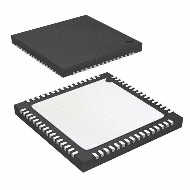
| 产品图片 |
|
| 产品型号 | LTC2369CMS-18#PBF |
| rohs | 无铅 / 符合限制有害物质指令(RoHS)规范要求 |
| 产品系列 | - |
| 产品培训模块 | http://www.digikey.cn/PTM/IndividualPTM.page?site=cn&lang=zhs&ptm=25823 |
| 位数 | 18 |
| 供应商器件封装 | 16-MSOP |
| 其它名称 | LTC2369CMS18PBF |
| 包装 | 管件 |
| 安装类型 | 表面贴装 |
| 封装/外壳 | 16-TFSOP(0.118",3.00mm 宽) |
| 工作温度 | 0°C ~ 70°C |
| 数据接口 | SPI |
| 标准包装 | 37 |
| 特性 | - |
| 电压源 | 模拟和数字 |
| 转换器数 | 1 |
| 输入数和类型 | 1 个伪差分,单极 |
| 配用 | /product-detail/zh/DC1813A-E/DC1813A-E-ND/3029530 |
| 采样率(每秒) | 1.6M |


- 商务部:美国ITC正式对集成电路等产品启动337调查
- 曝三星4nm工艺存在良率问题 高通将骁龙8 Gen1或转产台积电
- 太阳诱电将投资9.5亿元在常州建新厂生产MLCC 预计2023年完工
- 英特尔发布欧洲新工厂建设计划 深化IDM 2.0 战略
- 台积电先进制程称霸业界 有大客户加持明年业绩稳了
- 达到5530亿美元!SIA预计今年全球半导体销售额将创下新高
- 英特尔拟将自动驾驶子公司Mobileye上市 估值或超500亿美元
- 三星加码芯片和SET,合并消费电子和移动部门,撤换高东真等 CEO
- 三星电子宣布重大人事变动 还合并消费电子和移动部门
- 海关总署:前11个月进口集成电路产品价值2.52万亿元 增长14.8%


PDF Datasheet 数据手册内容提取
LTC2369-18 18-Bit, 1.6Msps, Pseudo- Differential Unipolar SAR ADC with 96.5dB SNR FEATURES DESCRIPTION n 1.6Msps Throughput Rate The LTC®2369-18 is a low noise, low power, high speed n ±2.5LSB INL (Max) 18-bit successive approximation register (SAR) ADC. n Guaranteed 18-Bit No Missing Codes Operating from a 2.5V supply, the LTC2369-18 has a 0V n Low Power: 18mW at 1.6Msps, 18μW at 1.6ksps to V pseudo-differential unipolar input range with V REF REF n 96.5dB SNR (Typ) at fIN = 2kHz ranging from 2.5V to 5.1V. The LTC2369-18 consumes only n –120dB THD (Typ) at fIN = 2kHz 18mW and achieves ±2.5LSB INL maximum, no missing n Guaranteed Operation to 125°C codes at 18 bits with 96.5dB SNR. n 2.5V Supply The LTC2369-18 has a high speed SPI-compatible serial n Pseudo-Differential Unipolar Input Range: 0V to V REF interface that supports 1.8V, 2.5V, 3.3V and 5V logic while n V Input Range from 2.5V to 5.1V REF also featuring a daisy-chain mode. The fast 1.6Msps n No Pipeline Delay, No Cycle Latency throughput with no cycle latency makes the LTC2369-18 n 1.8V to 5V I/O Voltages ideally suited for a wide variety of high speed applications. n SPI-Compatible Serial I/O with Daisy-Chain Mode An internal oscillator sets the conversion time, easing exter- n Internal Conversion Clock nal timing considerations. The LTC2369-18 automatically n 16-Lead MSOP and 4mm × 3mm DFN Packages powers down between conversions, leading to reduced APPLICATIONS power dissipation that scales with the sampling rate. L, LT, LTC, LTM, Linear Technology and the Linear logo are registered trademarks and n Medical Imaging SoftSpan is a trademark of Linear Technology Corporation. All other trademarks are the n High Speed Data Acquisition property of their respective owners. Protected by U.S. Patents including 7705765. n Portable or Compact Instrumentation n Industrial Process Control n Low Power Battery-Operated Instrumentation n ATE TYPICAL APPLICATION 32k Point FFT f = 1.6Msps, f = 2kHz S IN 0 2.5V 1.8V TO 5V SNR = 96.5dB –20 THD = –127dB 10μF 0.1μF SINAD = 96.5dB –40 SFDR = 134dB VR0EVF +LT®6202 5.1Ω IN+ VDD OVDD RCDHLA/SINDI E (dBFS) ––6800 D – 10nF LTC2369-18 SSDCOK LITU–100 IN– BUSY MP–120 CNV SAMPLE CLOCK A RREEFF GND –140 236918 TA01a 2.5V TO 5.1V –160 47μF (X5R, 0805 SIZE) –180 0 100 200 300 400 500 600 700 800 FREQUENCY (kHz) 236918 TA01b 236918fa 1
LTC2369-18 ABSOLUTE MAXIMUM RATINGS (Notes 1, 2) Supply Voltage (V ) ...............................................2.8V Power Dissipation ..............................................500mW DD Supply Voltage (OV ) ................................................6V Operating Temperature Range DD Reference Input (REF) .................................................6V LTC2369C ................................................0°C to 70°C Analog Input Voltage (Note 3) LTC2369I .............................................–40°C to 85°C IN+, IN– .........................(GND – 0.3V) to (REF + 0.3V) LTC2369H ..........................................–40°C to 125°C Digital Input Voltage Storage Temperature Range ..................–65°C to 150°C (Note 3) ..........................(GND – 0.3V) to (OV + 0.3V) DD Digital Output Voltage (Note 3) ..........................(GND – 0.3V) to (OV + 0.3V) DD PIN CONFIGURATION TOP VIEW CHAIN 1 16 GND TOP VIEW VDD 2 15 OVDD CHAIN 1 16 GND GND 3 14 SDO VDD 2 15 OVDD IN+ 4 17 13 SCK GND 3 14 SDO IN– 5 GND 12 RDL/SDI IINN+– 45 1132 SRCDKL/SDI GND 6 11 BUSY GND 6 11 BUSY REF 7 10 GND REF 7 10 GND REF 8 9 CNV REF 8 9 CNV MS PACKAGE DE PACKAGE 16-LEAD PLASTIC MSOP 16-LEAD (4mm (cid:119) 3mm) PLASTIC DFN TJMAX = 150°C, θJA = 110°C/W TJMAX = 150°C, θJA = 40°C/W EXPOSED PAD (PIN 17) IS GND, MUST BE SOLDERED TO PCB ORDER INFORMATION LEAD FREE FINISH TAPE AND REEL PART MARKING* PACKAGE DESCRIPTION TEMPERATURE RANGE LTC2369CMS-18#PBF LTC2369CMS-18#TRPBF 236918 16-Lead Plastic MSOP 0°C to 70°C LTC2369IMS-18#PBF LTC2369IMS-18#TRPBF 236918 16-Lead Plastic MSOP –40°C to 85°C LTC2369HMS-18#PBF LTC2369HMS-18#TRPBF 236918 16-Lead Plastic MSOP –40°C to 125°C LTC2369CDE-18#PBF LTC2369CDE-18#TRPBF 23698 16-Lead (4mm × 3mm) Plastic DFN 0°C to 70°C LTC2369IDE-18#PBF LTC2369IDE-18#TRPBF 23698 16-Lead (4mm × 3mm) Plastic DFN –40°C to 85°C Consult LTC Marketing for parts specified with wider operating temperature ranges. *The temperature grade is identified by a label on the shipping container. Consult LTC Marketing for information on non-standard lead based finish parts. For more information on lead free part marking, go to: http://www.linear.com/leadfree/ For more information on tape and reel specifications, go to: http://www.linear.com/tapeandreel/ 236918fa 2
LTC2369-18 ELECTRICAL CHARACTERISTICS The l denotes the specifications which apply over the full operating temperature range, otherwise specifications are at T = 25°C. (Note 4) A SYMBOL PARAMETER CONDITIONS MIN TYP MAX UNITS V + Absolute Input Range (IN+) (Note 5) l –0.1 V + 0.1 V IN REF V – Absolute Input Range (IN–) (Note 5) l –0.1 0.1 V IN V + – V – Input Differential Voltage Range V = V + – V – l 0 V V IN IN IN IN IN REF I Analog Input Leakage Current l ±1 μA IN C Analog Input Capacitance Sample Mode 45 pF IN Hold Mode 5 pF CMRR Input Common Mode Rejection Ratio f = 800kHz 80 dB IN CONVERTER CHARACTERISTICS The l denotes the specifications which apply over the full operating temperature range, otherwise specifications are at T = 25°C. (Note 4) A SYMBOL PARAMETER CONDITIONS MIN TYP MAX UNITS Resolution l 18 Bits No Missing Codes l 18 Bits Transition Noise 1.3 LSB RMS INL Integral Linearity Error (Note 6) l –2.5 ±0.5 2.5 LSB DNL Differential Linearity Error l –0.5 ±0.1 0.5 LSB ZSE Zero-Scale Error (Note 7) l –11 0 11 LSB Zero-Scale Error Drift 0.04 LSB/°C FSE Full-Scale Error (Note 7) l –50 ±5 50 LSB Full-Scale Error Drift ±0.15 ppm/°C DYNAMIC ACCURACY The l denotes the specifications which apply over the full operating temperature range, otherwise specifications are at T = 25°C and A = –1dBFS. (Notes 4, 8) A IN SYMBOL PARAMETER CONDITIONS MIN TYP MAX UNITS SINAD Signal-to-(Noise + Distortion) Ratio f = 2kHz, V = 5V l 92.2 96.5 dB IN REF f = 2kHz, V = 5V, (H-Grade) l 91.7 96.5 dB IN REF SNR Signal-to-Noise Ratio f = 2kHz, V = 5V l 92.6 96.5 dB IN REF f = 2kHz, V = 2.5V l 87 90.7 dB IN REF f = 2kHz, V = 5V, (H-Grade) l 92 96.5 dB IN REF f = 2kHz, V = 2.5V, (H-Grade) l 86.4 90.7 dB IN REF THD Total Harmonic Distortion f = 2kHz, V = 5V l –120 –103 dB IN REF f = 2kHz, V = 2.5V l –107 –103 dB IN REF SFDR Spurious Free Dynamic Range f = 2kHz, V = 5V l 103 122 dB IN REF –3dB Input Bandwidth 34 MHz Aperture Delay 500 ps Aperture Jitter 4 ps Transient Response Full-Scale Step 200 ns 236918fa 3
LTC2369-18 REFERENCE INPUT The l denotes the specifications which apply over the full operating temperature range, otherwise specifications are at T = 25°C. (Note 4) A SYMBOL PARAMETER CONDITIONS MIN TYP MAX UNITS V Reference Voltage (Note 5) l 2.5 5.1 V REF I Reference Input Current (Note 9) l 0.85 1.1 mA REF DIGITAL INPUTS AND DIGITAL OUTPUTS The l denotes the specifications which apply over the full operating temperature range, otherwise specifications are at T = 25°C. (Note 4) A SYMBOL PARAMETER CONDITIONS MIN TYP MAX UNITS V High Level Input Voltage l 0.8 • OV V IH DD V Low Level Input Voltage l 0.2 • OV V IL DD I Digital Input Current V = 0V to OV l –10 10 μA IN IN DD C Digital Input Capacitance 5 pF IN V High Level Output Voltage I = –500μA l OV –0.2 V OH O DD V Low Level Output Voltage I = 500μA l 0.2 V OL O I Hi-Z Output Leakage Current V = 0V to OV l –10 10 μA OZ OUT DD I Output Source Current V = 0V –10 mA SOURCE OUT I Output Sink Current V = OV 10 mA SINK OUT DD POWER REQUIREMENTS The l denotes the specifications which apply over the full operating temperature range, otherwise specifications are at T = 25°C. (Note 4) A SYMBOL PARAMETER CONDITIONS MIN TYP MAX UNITS V Supply Voltage l 2.375 2.5 2.625 V DD OV Supply Voltage l 1.71 5.25 V DD I Supply Current 1.6Msps Sample Rate l 7.2 8.6 mA VDD I Supply Current 1.6Msps Sample Rate (C = 20pF) 0.7 mA OVDD L I Power Down Mode Conversion Done (I + I + I , V > 2V) l 0.9 90 μA PD VDD OVDD REF REF I Power Down Mode Conversion Done (I + I + I , V > 2V, H-Grade) l 0.9 140 μA PD VDD OVDD REF REF P Power Dissipation 1.6Msps Sample Rate 18 21.5 mW D Power Down Mode Conversion Done (I + I + I , V > 2V) 2.25 225 μW VDD OVDD REF REF Power Down Mode Conversion Done (I + I + I , V > 2V, H-Grade) 2.25 315 μW VDD OVDD REF REF ADC TIMING CHARACTERISTICS The l denotes the specifications which apply over the full operating temperature range, otherwise specifications are at T = 25°C. (Note 4) A SYMBOL PARAMETER CONDITIONS MIN TYP MAX UNITS f Maximum Sampling Frequency l 1.6 Msps SMPL t Conversion Time l 360 412 ns CONV t Acquisition Time t = t – t – t (Note 10) l 200 ns ACQ ACQ CYC CONV BUSYLH t Time Between Conversions l 625 ns CYC t CNV High Time l 20 ns CNVH tBUSYLH CNV↑ to BUSY Delay CL = 20pF l 13 ns t Minimum Low Time for CNV (Note 11) l 20 ns CNVL tQUIET SCK Quiet Time from CNV↑ (Note 10) l 20 ns t SCK Period (Notes 11, 12) l 10 ns SCK t SCK High Time l 4 ns SCKH 236918fa 4
LTC2369-18 ADC TIMING CHARACTERISTICS The l denotes the specifications which apply over the full operating temperature range, otherwise specifications are at T = 25°C. (Note 4) A SYMBOL PARAMETER CONDITIONS MIN TYP MAX UNITS t SCK Low Time l 4 ns SCKL tSSDISCK SDI Setup Time From SCK↑ (Note 11) l 4 ns tHSDISCK SDI Hold Time From SCK↑ (Note 11) l 1 ns t SCK Period in Chain Mode t = t + t (Note 11) l 13.5 ns SCKCH SCKCH SSDISCK DSDO tDSDO SDO Data Valid Delay from SCK↑ CL = 20pF (Note 11) l 9.5 ns tHSDO SDO Data Remains Valid Delay from SCK↑ CL = 20pF (Note 10) l 1 ns tDSDOBUSYL SDO Data Valid Delay from BUSY↓ CL = 20pF (Note 10) l 5 ns tEN Bus Enable Time After RDL↓ (Note 11) l 16 ns tDIS Bus Relinquish Time After RDL↑ (Note 11) l 13 ns Note 1: Stresses beyond those listed under Absolute Maximum Ratings Note 7: Zero-scale error is the offset voltage measured from 0.5LSB may cause permanent damage to the device. Exposure to any Absolute when the output code flickers between 00 0000 0000 0000 0000 and Maximum Rating condition for extended periods may effect device 00 0000 0000 0000 0001. Full-scale error is the deviation of the last code reliability and lifetime. transition from ideal and includes the effect of offset error. Note 2: All voltage values are with respect to ground. Note 8: All specifications in dB are referred to a full-scale 5V input with a Note 3: When these pin voltages are taken below ground or above REF or 5V reference voltage. OV , they will be clamped by internal diodes. This product can handle Note 9: f = 1.6MHz, I varies proportionately with sample rate. DD SMPL REF input currents up to 100mA below ground or above REF or OVDD without Note 10: Guaranteed by design, not subject to test. latch-up. Note 11: Parameter tested and guaranteed at OV = 1.71V, OV = 2.5V DD DD Note 4: VDD = 2.5V, OVDD = 2.5V, REF = 5V, fSMPL = 1.6MHz. and OVDD = 5.25V. Note 5: Recommended operating conditions. Note 12: t of 10ns maximum allows a shift clock frequency up to SCK Note 6: Integral nonlinearity is defined as the deviation of a code from a 100MHz for rising capture. straight line passing through the actual endpoints of the transfer curve. The deviation is measured from the center of the quantization band. 0.8*OVDD tWIDTH 0.2*OVDD tDELAY tDELAY 50% 50% 0.8*OVDD 0.8*OVDD 236918 F01 0.2*OVDD 0.2*OVDD Figure 1. Voltage Levels for Timing Specifications 236918fa 5
LTC2369-18 TYPICAL PERFORMANCE CHARACTERISTICS T = 25°C, V = 2.5V, OV = 2.5V, REF = 5V, A DD DD f = 1.6Msps, unless otherwise noted. SMPL Integral Nonlinearity Differential Nonlinearity vs Output Code vs Output Code DC Histogram 2.0 0.5 40000 (cid:88) = 1.3 0.4 1.5 35000 0.3 1.0 30000 INL ERROR (LSB) –000...055 DNL ERROR (LSB)––00000.....21021 COUNTS212550000000000 –1.0 10000 –0.3 –1.5 –0.4 5000 –2.0 –0.5 0 0 65536 131072 196608 262144 0 65536 131072 196608 262144 131067131069131071131073131075131077 OUTPUT CODE OUTPUT CODE CODE 236918 G01 236918 G02 236918 G03 32k Point FFT f = 1.6Msps, THD, Harmonics S f = 2kHz SNR, SINAD vs Input Frequency vs Input Frequency IN 0 100 –60 SNR = 96.5dB –20 THD = –127dB –70 SINAD = 96.5dB 95 –40 SFDR = 134dB SNR S) –80 THD dBFS) –60 dBFS) 90 SINAD D (dBF–1–0900 2ND E ( –80 D ( TH 3RD MPLITUD––110200 NR, SINA 8850 MONICS, ––112100 A S R–130 A –140 H –140 75 –160 –150 –180 70 –160 0 100 200 300 400 500 600 700 800 0 25 50 75 100 125 150 175 200 0 25 50 75 100 125 150 175 200 FREQUENCY (kHz) FREQUENCY (kHz) FREQUENCY (kHz) 236918 G04 236918 G05 236918 G06 SNR, SINAD vs Input level, SNR, SINAD vs Reference THD, Harmonics vs Reference f = 2kHz Voltage, f = 2kHz Voltage, f = 2kHz IN IN IN 98.0 97 –100 –105 96 97.5 SNR –110 S) NR, SINAD (dBFS)999667...050 SSINNARD NR, SINAD (dBFS) 999543 SINAD MONICS, THD (dBF––––111123210055 2ND3TRHDD S S 92 AR–135 H –140 95.5 91 –145 95.0 90 –150 –40 –30 –20 –10 0 2.5 3 3.5 4 4.5 5 2.5 3 3.5 4 4.5 5 INPUT LEVEL (dB) REFERENCE VOLTAGE (V) REFERENCE VOLTAGE (V) 236918 G07 236918 G08 236918 G09 236918fa 6
LTC2369-18 TYPICAL PERFORMANCE CHARACTERISTICS T = 25°C, V = 2.5V, OV = 2.5V, REF = 5V, A DD DD f = 1.6Msps, unless otherwise noted. SMPL SNR, SINAD vs Temperature, THD, Harmonics vs Temperature, f = 2kHz f = 2kHz INL/DNL vs Temperature IN IN 98.0 –110 1.0 97.5 –115 MAX INL SNR, SINAD (dBFS)9999965756.....55000 SINADSNR HARMONICS, THD (dBFS)––––111123325500 3RD 2NTDHD INL/DNL ERROR (LSB)–00..550 MMMAIINXN DDINNNLLL –140 94.5 94.0 –145 –1.0 –55 –35 –15 5 25 45 65 85 105 125 –55 –35 –15 5 25 45 65 85 105 125 –55 –35 –15 5 25 45 65 85 105 125 TEMPERATURE (°C) TEMPERATURE (°C) TEMPERATURE (°C) 236918 G10 236918 G11 236918 G12 Full-Scale Error vs Temperature Offset Error vs Temperature Supply Current vs Temperature 20 10 8 8 IVDD 15 7 6 mA) ULL-SCALE ERROR (LSB)–1–105500 OFFSET ERROR (LSB) ––44202 WER SUPPLY CURRENT ( 53624 F –6 O –15 –8 P 1 IREF IOVDD –20 –10 0 –55 –35 –15 5 25 45 65 85 105 125 –55–35 –15 5 25 45 65 85 105 125 –55 –35 –15 5 25 45 65 85 105 125 TEMPERATURE (°C) TEMPERATURE (°C) TEMPERATURE (°C) 236918 G13 236918 G14 236918 G15 Reference Current Shutdown Current vs Temperature CMRR vs Input Frequency vs Reference Voltage 45 100 0.9 IVDD + IOVDD + IREF 40 0.8 95 μA) 35 A) 0.7 WN CURRENT ( 322005 MRR (dB) 8950 E CURRENT (m 000...456 DO C NC R- 15 80 RE 0.3 E E W F O 10 RE 0.2 P 75 5 0.1 0 70 0 –55 –35 –15 5 25 45 65 85 105 125 0 100 200 300 400 500 600 700 800 2.5 3 3.5 4 4.5 5 TEMPERATURE (°C) FREQUENCY (kHz) REFERENCE VOLTAGE (V) 236918 G16 236918 G17 236918 G18 236918fa 7
LTC2369-18 PIN FUNCTIONS CHAIN (Pin 1): Chain Mode Selector Pin. When low, the BUSY (Pin 11): BUSY Indicator. Goes high at the start of LTC2369-18 operates in normal mode and the RDL/SDI a new conversion and returns low when the conversion input pin functions to enable or disable SDO. When high, has finished. Logic levels are determined by OV . DD the LTC2369-18 operates in chain mode and the RDL/SDI RDL/SDI (Pin 12): When CHAIN is low, the part is in nor- pin functions as SDI, the daisy-chain serial data input. mal mode and the pin is treated as a bus enabling input. Logic levels are determined by OV . DD When CHAIN is high, the part is in chain mode and the V (Pin 2): 2.5V Power Supply. The range of V is pin is treated as a serial data input pin where data from DD DD 2.375V to 2.625V. Bypass V to GND with a 10μF ceramic another ADC in the daisy chain is input. Logic levels are DD capacitor. determined by OV . DD GND (Pins 3, 6, 10 and 16): Ground. SCK (Pin 13): Serial Data Clock Input. When SDO is enabled, the conversion result or daisy-chain data from another IN+ (Pin 4): Analog Input. IN+ operates differential with ADC is shifted out on the rising edges of this clock MSB respect to IN– with an IN+-IN– range of 0V to V . REF first. Logic levels are determined by OV . DD IN– (Pin 5): Analog Ground Sense. IN– has an input range SDO (Pin 14): Serial Data Output. The conversion result of ±100mV with respect to GND and must be tied to the or daisy-chain data is output on this pin on each rising ground plane or a remote ground sense. edge of SCK MSB first. The output data is in straight binary REF (Pins 7, 8): Reference Inputs. The range of REF is 2.5V format. Logic levels are determined by OV . DD to 5.1V. This pin is referred to the GND pin and should be OV (Pin 15): I/O Interface Digital Power. The range of decoupled closely to the pin with a 47μF ceramic capacitor DD OV is 1.71V to 5.25V. This supply is nominally set to (X5R, 0805 size). DD the same supply as the host interface (1.8V, 2.5V, 3.3V, CNV (Pin 9): Convert Input. A rising edge on this input or 5V). Bypass OV to GND with a 0.1μF capacitor. DD powers up the part and initiates a new conversion. Logic GND (Exposed Pad Pin 17, DFN Package Only): Ground. levels are determined by OV . DD Exposed pad must be soldered directly to the ground plane. 236918fa 8
LTC2369-18 FUNCTIONAL BLOCK DIAGRAM VDD = 2.5V REF = 5V OVDD = 1.8V to 5V CHAIN IN+ + SDO SPI RDL/SDI 18-BIT SAMPLING ADC PORT SCK IN– – CNV CONTROL LOGIC BUSY GND 236918 BD TIMING DIAGRAM Conversion Timing Using the Serial Interface CHAIN, RDL/SDI = 0 CNV BUSY CONVERT POWER-DOWN AND ACQUIRE SCK SDO D17 D16 D15 D14 D13 D12 D11 D10 D9 D8 D7 D6 D5 D4 D3 D2 D1 D0 236918 TD01 236918fa 9
LTC2369-18 APPLICATIONS INFORMATION OVERVIEW 1LSB = FS/262144 111...111 The LTC2369-18 is a low noise, low power, high speed 18-bit 111...110 successive approximation register (SAR) ADC. Operating 111...101 from a single 2.5V supply, the LTC2369-18 supports a DE 111...100 O C 0V to VREF pseudo-differential unipolar input range with UT P V ranging from 2.5V to 5.1V, making it ideal for high T REF U UNIPOLAR O performance applications which require a wide dynamic ZERO 000...011 range. The LTC2369-18 achieves ±2.5LSB INL max, no 000...010 missing codes at 18 bits and 96.5dB SNR. 000...001 000...000 Fast 1.6Msps throughput with no cycle latency makes 0V 1 FS – 1LSB LSB the LTC2369-18 ideally suited for a wide variety of high INPUT VOLTAGE (V) 236918 F02 speed applications. An internal oscillator sets the con- Figure 2. LTC2369-18 Transfer Function version time, easing external timing considerations. The LTC2369-18 dissipates only 18mW at 1.6Msps, while an ANALOG INPUT auto power-down feature is provided to further reduce The analog inputs of the LTC2369-18 are pseudo-differential power dissipation during inactive periods. in order to reduce any unwanted signal that is common to both inputs. The analog inputs can be modeled by the CONVERTER OPERATION equivalent circuit shown in Figure 3. The diodes at the input provide ESD protection. In the acquisition phase, each The LTC2369-18 operates in two phases. During the ac- input sees approximately 45pF (C ) from the sampling IN quisition phase, the charge redistribution capacitor D/A CDAC in series with 40Ω (R ) from the on-resistance ON converter (CDAC) is connected to the IN+ and IN– pins to of the sampling switch. The IN+ input draws a current sample the pseudo-differential analog input voltage. A ris- spike while charging the C capacitor during acquisition. IN ing edge on the CNV pin initiates a conversion. During the During conversion, the analog inputs draw only a small conversion phase, the 18-bit CDAC is sequenced through a leakage current. successive approximation algorithm, effectively comparing the sampled input with binary-weighted fractions of the REF CIN reference voltage (e.g. VREF/2, VREF/4 … VREF/262144) RON 45pF 40Ω using the differential comparator. At the end of conver- IN+ sion, the CDAC output approximates the sampled analog input. The ADC control logic then prepares the 18-bit BIAS digital output code for serial transfer. REF CIN VOLTAGE RON 45pF 40Ω IN– 236918 F03 TRANSFER FUNCTION The LTC2369-18 digitizes the full-scale voltage of REF into 218 levels, resulting in an LSB size of 19μV with Figure 3. The Equivalent Circuit for the REF = 5V. The ideal transfer function is shown in Figure 2. Differential Analog Input of the LTC2369-18 The output data is in straight binary format. 236918fa 10
LTC2369-18 APPLICATIONS INFORMATION INPUT DRIVE CIRCUITS High quality capacitors and resistors should be used in the RC filters since these components can add distortion. NPO A low impedance source can directly drive the high im- and silver mica type dielectric capacitors have excellent pedance input of the LTC2369-18 without gain error. A linearity. Carbon surface mount resistors can generate high impedance source should be buffered to minimize distortion from self heating and from damage that may settling time during acquisition and to optimize the dis- occur during soldering. Metal film surface mount resistors tortion performance of the ADC. Minimizing settling time are much less susceptible to both problems. is important even for DC inputs, because the ADC input draws a current spike when entering acquisition. Pseudo-Differential Unipolar Inputs For best performance, a buffer amplifier should be used For most applications, we recommend the low power to drive the analog input of the LTC2369-18. The ampli- LT6202 ADC driver to drive the LTC2369-18. With a low fier provides low output impedance, which produces fast noise density of 1.9nV/√Hz and a low supply current of settling of the analog signal during the acquisition phase. 3mA, the LT6202 is flexible and may be configured to It also provides isolation between the signal source and convert signals of various amplitudes to the 0V to 5V input the current spike the ADC input draws. range of the LTC2369-18. Input Filtering To achieve the full distortion performance of the LTC2369-18, a low distortion single-ended signal source The noise and distortion of the buffer amplifier and signal driven through the LT6202 configured as a unity-gain buf- source must be considered since they add to the ADC noise fer as shown in Figure 4 can be used to get the full data and distortion. Noisy input signals should be filtered prior sheet THD specification of –120dB. to the buffer amplifier input with an appropriate filter to minimize noise. The simple 1-pole RC lowpass filter (LPF1) The LT6202 can also be used to buffer and convert large shown in Figure 4 is sufficient for many applications. true bipolar signals which swing below ground to the 0V to 5V input range of the LTC2369-18. Figure 5a shows the LPF1 LT6202 being used to convert a ±10V true bipolar signal LPF2 VREF 50Ω + for use by the LTC2369-18. In this case, the LT6202 is 0V 5.1Ω 66nF LT6202 IN+ configured as an inverting amplifier stage, which acts to – 10nF LTC2369-18 attenuate and level shift the input signal to the 0V to 5V input BW = 48kHz IN– range of the LTC2369-18. In the inverting configuration, the single-ended input signal source no longer directly drives BW = 3.2MHz 236918 F04 a high impedance input. The input impedance is instead Figure 4. Input Signal Chain set by resistor R . R must be chosen carefully based on IN IN the source impedance of the signal source. Higher values Another filter network consisting of LPF2 should be used of R tend to degrade both the noise and distortion of IN between the buffer and ADC input to both minimize the the LT6202 and LTC2369-18 as a system. Table 1 shows noise contribution of the buffer and to help minimize distur- the resulting SNR and THD for several values of R , R1, IN bances reflected into the buffer from sampling transients. R2, R3 and R4 in this configuration. Figure 5b shows the Long RC time constants at the analog inputs will slow resulting FFT when using the LT6202 as shown in Figure 5a. down the settling of the analog inputs. Therefore, LPF2 requires a wider bandwidth than LPF1. A buffer amplifier with a low noise density must be selected to minimize degradation of the SNR. 236918fa 11
LTC2369-18 APPLICATIONS INFORMATION VCM = VREF/2 200pF ADC REFERENCE The LTC2369-18 requires an external reference to define R2 R4 499Ω 402Ω its input range. A low noise, low temperature drift refer- 3 + ence is critical to achieving the full datasheet performance R3 5V 10μF LT6202 1 2k of the ADC. Linear Technology offers a portfolio of high 0V 4 – performance references designed to meet the needs of RIN R1 10V 2k 499Ω many applications. With its small size, low power and 0V –10V 200pF high accuracy, the LTC6655-5 is particularly well suited for 236918 F05a use with the LTC2369-18. The LTC6655-5 offers 0.025% (max) initial accuracy and 2ppm/°C (max) temperature Figure 5a. LT6202 Converting a ±10V Bipolar Signal coefficient for high precision applications. The LTC6655-5 to a 0V to 5V Input Signal is fully specified over the H-grade temperature range and 0 complements the extended temperature operation of the SNR = 96.1dB –20 THD = –97.3dB LTC2369-18 up to 125°C. We recommend bypassing the SINAD = 92.7dB –40 SFDR = 97.5dB LTC6655-5 with a 47μF ceramic capacitor (X5R, 0805 size) FS) close to the REF pin. B –60 d E ( UD –80 The REF pin of the LTC2369-18 draws charge (QCONV) from T LI the 47μF bypass capacitor during each conversion cycle. P–100 M A The reference replenishes this charge with a DC current, –120 I = Q /t . The DC current draw of the REF pin, REF CONV CYC –140 I , depends on the sampling rate and output code. If REF –160 the LTC2369-18 is used to continuously sample a signal 1 100 200 300 400 500 600 700 800 FREQUENCY (kHz) at a constant rate, the LTC6655-5 will keep the deviation 236918 F05b of the reference voltage over the entire code span to less Figure 5b. 32k Point FFT Plot with fIN = 2kHz than 0.5LSBs. for Circuit Shown in Figure 5a When idling, the REF pin on the LTC2369-18 draws only a small leakage current (< 1μA). In applications where a Table 1. SNR, THD vs RIN for ±10V Input Signal burst of samples is taken after idling for long periods as RIN R1 R2 R3 R4 SNR THD shown in Figure 6, IREF quickly goes from approximately (Ω) (Ω) (Ω) (Ω) (Ω) (dB) (dB) 0μA to a maximum of 1.1mA at 1.6Msps. This step in DC 2k 499 499 2k 402 96.1 –97.3 current draw triggers a transient response in the reference 10k 2.49k 2.49k 10k 2k 96 –92 that must be considered since any deviation in the refer- 100k 24.9k 24.9k 100k 20k 93.8 –93.5 ence output voltage will affect the accuracy of the output CNV 236918 F06 IDLE IDLE PERIOD PERIOD Figure 6. CNV Waveform Showing Burst Sampling 236918fa 12
LTC2369-18 APPLICATIONS INFORMATION code. In applications where the transient response of the the RMS amplitude of all other frequency components reference is important, the fast settling LTC6655-5 refer- except the first five harmonics and DC. Figure 8 shows ence is also recommended. that the LTC2369-18 achieves a typical SNR of 96.5dB at a 1.6MHz sampling rate with a 2kHz input. In applications where power management is critical and the external reference may be powered down, it is rec- 0 SNR = 96.5dB ommended that REF is kept greater than 2V in order to –20 THD = –127dB guarantee a maximum shutdown current of 140μA. In such SINAD = 96.5dB –40 SFDR = 134dB applications, a Schottky diode can be placed between REF S) –60 F and VDD, as shown in Figure 7. E (dB –80 D U T–100 LI P M–120 A REF VDD –140 LTC2369-18 –160 –180 0 100 200 300 400 500 600 700 800 FREQUENCY (kHz) 236918 F07 236918 F08 Figure 7. A Schottky Diode Between REF and V Maintains DD Figure 8. 32k Point FFT with f = 2kHz of the LTC2369-18 REF > 2V for Applications Where the Reference May Be IN Powered Down Total Harmonic Distortion (THD) DYNAMIC PERFORMANCE Total Harmonic Distortion (THD) is the ratio of the RMS sum of all harmonics of the input signal to the fundamental itself. Fast Fourier Transform (FFT) techniques are used to test The out-of-band harmonics alias into the frequency band the ADC’s frequency response, distortion and noise at the between DC and half the sampling frequency (f /2). rated throughput. By applying a low distortion sine wave SMPL THD is expressed as: and analyzing the digital output using an FFT algorithm, the ADC’s spectral content can be examined for frequen- V22 +V32 +V42 +…+V2 cies outside the fundamental. The LTC2369-18 provides THD=20log N guaranteed tested limits for both AC distortion and noise V1 measurements. where V1 is the RMS amplitude of the fundamental fre- quency and V2 through V are the amplitudes of the second Signal-to-Noise and Distortion Ratio (SINAD) N through Nth harmonics. The signal-to-noise and distortion ratio (SINAD) is the ratio between the RMS amplitude of the fundamental input POWER CONSIDERATIONS frequency and the RMS amplitude of all other frequency components at the A/D output. The output is band-limited The LTC2369-18 provides two power supply pins: the to frequencies from above DC and below half the sampling 2.5V power supply (VDD), and the digital input/output frequency. Figure 8 shows that the LTC2369-18 achieves interface power supply (OVDD). The flexible OVDD supply a typical SINAD of 96.5dB at a 1.6MHz sampling rate with allows the LTC2369-18 to communicate with any digital a 2kHz input. logic operating between 1.8V and 5V, including 2.5V and 3.3V systems. Signal-to-Noise Ratio (SNR) The signal-to-noise ratio (SNR) is the ratio between the RMS amplitude of the fundamental input frequency and 236918fa 13
LTC2369-18 APPLICATIONS INFORMATION Power Supply Sequencing power down, disable SDO and turn off SCK. The auto power-down feature will reduce the power dissipation of The LTC2369-18 does not have any specific power supply the LTC2369-18 as the sampling frequency is reduced. sequencing requirements. Care should be taken to adhere Since power is consumed only during a conversion, the to the maximum voltage relationships described in the LTC2369-18 remains powered down for a larger fraction of Absolute Maximum Ratings section. The LTC2369-18 the conversion cycle (t ) at lower sample rates, thereby has a power-on-reset (POR) circuit that will reset the CYC reducing the average power dissipation which scales with LTC2369-18 at initial power-up or whenever the power the sampling rate as shown in Figure 9. supply voltage drops below 1V. Once the supply voltage re-enters the nominal supply voltage range, the POR will reinitialize the ADC. No conversions should be initiated DIGITAL INTERFACE until 20μs after a POR event to ensure the reinitialization The LTC2369-18 has a serial digital interface. The flexible period has ended. Any conversions initiated before this OV supply allows the LTC2369-18 to communicate with DD time will produce invalid results. any digital logic operating between 1.8V and 5V, including 2.5V and 3.3V systems. TIMING AND CONTROL The serial output data is clocked out on the SDO pin when an external clock is applied to the SCK pin if SDO is enabled. CNV Timing Clocking out the data after the conversion will yield the The LTC2369-18 conversion is controlled by CNV. A ris- best performance. With a shift clock frequency of at least ing edge on CNV will start a conversion and power up the 100MHz, a 1.6Msps throughput is still achieved. The serial LTC2369-18. Once a conversion has been initiated, it cannot output data changes state on the rising edge of SCK and be restarted until the conversion is complete. For optimum can be captured on the falling edge or next rising edge of performance, CNV should be driven by a clean low jitter SCK. D17 remains valid till the first rising edge of SCK. signal. Converter status is indicated by the BUSY output The serial interface on the LTC2369-18 is simple and which remains high while the conversion is in progress. straightforward to use. The following sections describe the To ensure that no errors occur in the digitized results, any operation of the LTC2369-18. Several modes are provided additional transitions on CNV should occur within 40ns depending on whether a single or multiple ADCs share the from the start of the conversion or after the conversion SPI bus or are daisy chained. has been completed. Once the conversion has completed, the LTC2369-18 powers down and begins acquiring the 8 input signal. 7 A) m Internal Conversion Clock NT ( 6 E RR 5 The LTC2369-18 has an internal clock that is trimmed to CU IVDD Y 4 achieve a maximum conversion time of 412ns. With a min- PL P U 3 imum acquisition time of 200ns, throughput performance S R of 1.6Msps is guaranteed without any external adjustments. WE 2 PO IOVDD 1 IREF Auto Power-Down 0 0 200 400 600 800 1000120014001600 The LTC2369-18 automatically powers down after a SAMPLING RATE (kHz) conversion has been completed and powers up once a 236918 F09 new conversion is initiated on the rising edge of CNV. Figure 9. Power Supply Current of the LTC2369-18 During power down, data from the last conversion can Versus Sampling Rate be clocked out. To minimize power dissipation during 236918fa 14
LTC2369-18 TIMING DIAGRAMS Normal Mode, Single Device Figure 10 shows a single LTC2369-18 operated in normal mode with CHAIN and RDL/SDI tied to ground. With When CHAIN = 0, the LTC2369-18 operates in normal RDL/SDI grounded, SDO is enabled and the MSB(D17) of mode. In normal mode, RDL/SDI enables or disables the the new conversion data is available at the falling edge of serial data output pin SDO. If RDL/SDI is high, SDO is in BUSY. This is the simplest way to operate the LTC2369-18. high impedance. If RDL/SDI is low, SDO is driven. CONVERT CNV DIGITAL HOST CHAIN BUSY IRQ LTC2369-18 RDL/SDI SDO DATA IN SCK CLK POWER-DOWN CONVERT POWER-DOWN AND ACQUIRE CONVERT AND ACQUIRE CHAIN = 0 RDL/SDI = 0 tCYC tCNVH tCNVL CNV tACQ = tCYC – tCONV – tBUSYLH BUSY tCONV tACQ tBUSYLH tSCK tSCKH tQUIET SCK 1 2 3 16 17 18 tHSDO tSCKL tDSDOBUSYL tDSDO SDO D17 D16 D15 D1 D0 236918 F10 Figure 10. Using a Single LTC2369-18 in Normal Mode 236918fa 15
LTC2369-18 TIMING DIAGRAMS Normal Mode, Multiple Devices be used to allow only one LTC2369-18 to drive SDO at a time in order to avoid bus conflicts. As shown in Figure 11, Figure 11 shows multiple LTC2369-18 devices operating the RDL/SDI inputs idle high and are individually brought in normal mode (CHAIN = 0) sharing CNV, SCK and SDO. low to read data out of each device between conversions. By sharing CNV, SCK and SDO, the number of required When RDL/SDI is brought low, the MSB of the selected signals to operate multiple ADCs in parallel is reduced. device is output onto SDO. Since SDO is shared, the RDL/SDI input of each ADC must RDLB RDLA CONVERT CNV CNV CHAIN CHAIN BUSY IRQ LTC2369-18 LTC2369-18 DIGITAL HOST SDO SDO B A RDL/SDI RDL/SDI SCK SCK DATA IN CLK POWER-DOWN CONVERT POWER-DOWN AND ACQUIRE CONVERT AND ACQUIRE CHAIN = 0 tCNVL CNV tCONV BUSY tBUSYLH RDL/SDIA RDL/SDIB tSCK tSCKH tQUIET SCK 1 2 3 16 17 18 19 20 21 34 35 36 tHSDO tSCKL tDSDO tDIS tEN SDO Hi-Z Hi-Z Hi-Z D17A D16A D15A D1A D0A D17B D16B D15B D1B D0B 236918 F11 Figure 11. Normal Mode With Multiple Devices Sharing CNV, SCK and SDO 236918fa 16
LTC2369-18 TIMING DIAGRAMS Chain Mode, Multiple Devices number of converters. Figure 12 shows an example with two daisy-chained devices. The MSB of converter A will When CHAIN = OV , the LTC2369-18 operates in DD appear at SDO of converter B after 18 SCK cycles. The chain mode. In chain mode, SDO is always enabled and MSB of converter A is clocked in at the SDI/RDL pin of RDL/SDI serves as the serial data input pin (SDI) where converter B on the rising edge of the first SCK. daisy-chain data output from another ADC can be input. This is useful for applications where hardware constraints may limit the number of lines needed to interface to a large CONVERT OVDD OVDD CHAIN CNV CHAIN CNV DIGITAL HOST LTC2369-18 LTC2369-18 RDL/SDI SDO RDL/SDI BUSY IRQ A B SDO DATA IN SCK SCK CLK POWER-DOWN CONVERT POWER-DOWN AND ACQUIRE CONVERT AND ACQUIRE CHAIN = OVDD RDL/SDIA = 0 tCYC tCNVL CNV BUSY tCONV tBUSYLH tSCKCH tSCKH tQUIET SCK 1 2 3 16 17 18 19 20 34 35 36 tSCKL tSSDISCK tHSDO tHSDISCK tDSDO SDOA = RDL/SDIB D17A D16A D15A D1A D0A tDSDOBUSYL SDOB D17B D16B D15B D1B D0B D17A D16A D1A D0A 236918 F12 Figure 12. Chain Mode Timing Diagram 236918fa 17
LTC2369-18 BOARD LAYOUT To obtain the best performance from the LTC2369-18 Recommended Layout a printed circuit board is recommended. Layout for the The following is an example of a recommended PCB layout. printed circuit board (PCB) should ensure the digital and A single solid ground plane is used. Bypass capacitors to analog signal lines are separated as much as possible. In the supplies are placed as close as possible to the supply particular, care should be taken not to run any digital clocks pins. Low impedance common returns for these bypass or signals alongside analog signals or underneath the ADC. capacitors are essential to the low noise operation of the ADC. The analog input traces are screened by ground. For more details and information refer to DC1813A, the evaluation kit for the LTC2369-18. Partial Top Silkscreen 236918fa 18
LTC2369-18 BOARD LAYOUT Partial Layer 1 Component Side Partial Layer 2 Ground Plane 236918fa 19
LTC2369-18 BOARD LAYOUT Partial Layer 3 PWR Plane Partial Layer 4 Bottom Layer 236918fa 20
LTC2369-18 BOARD LAYOUT Partial Schematic of Demoboard D +3.3VC40.1μF U4NC7SVU04P5X5CNVST_332FROM CPL3 DB17 DB16 J2DGE 40-100 403836343230282624222018161412108642 236918 BL R133Ω +3.3VC30.1μF 12 CPD48R4+3.3VVGNDCC33Ω674R46CLR\PR\ØΩU3Q\QNL17SZ74C205C56347μF0.1μFR86.3V33Ω0805JP6DC590 DETECTFSTO CPLD1VREFCON-E2+3.3V393C130.8VREF37DB00.1μF35DB1HD1X3-100U633DB2OPTNC7SZ66P5X531DB3CNVV29DB4CC8912BA27DB5FCNVE13SCK25DB6RSCKOE423DB7SDO14SDO21DB8GNDBUSY11BUSY19DB9317DB1012RDRDL/SDI15DB1113DB12R7+3.3V11DB131k9DB14U97DB15C15NC7SZ04P5X550.1μF243CLKOUTC1611R13R1730.1μF1k2k U7C14R12R11R1024LC025-I/ST80.1μF4.99k4.99k4.99kVCCSCL6SCKSDA5WP7CNVARRAY3A2EEPROM2A11A0 VSS4 7 FER 8 DNG 1 U20LTC6655AHMS8-518SHDNGND27VOUT_FIN36OUT_SGND45GNDGND +3.3V C7C60.1μF10μF+2.5V6.3V C10C90.1μF10μF6.3V C395R160.01μF120ΩNPO4DDDD+VVINOC65OPTR19LTC2369-10805 NPO0Ω–INDDDNNN5R58GGGC40ØΩ0663OPT11NPOR38OPT 9V TOJ310VDC5901234SDO567891011121314 0V C110.1μF R31OPT R325.1Ω 45Ω 35PT 1 RØ RO O 9V T C58OPT C600.1μF +3.3V+3.3VC1C20.1μF0.1μF R355CLK33Ω442TO CPLD U8U233NC7SZ04P5XNC7SVU04P5X LINGDC +V U155LT6202CS53R32V+0Ω+IN13+OUT11C42–R915pFOPT4 C6110μF6.3V 2–V C55+V1μF–VC570.1μFC6310μF6.3VR40C43C59OPT0.1μF1μF C441μF C49R41OPTOPT +3.3V R21kC50.1μFJ12LKINR5R649.9Ω1k1206 COUPAC JP1HD1X3-100 C1712R1410μF0Ω R15C18OPTOPT +2.5V C81μF JP2CM1V2REF/2 3EXTE7HD1X3-100MC461μF COUPLINGAC DC JP5HD1X3-100 123R390Ω C47C48OPT10μF6.3V C J4+AIN EXT_C J8–AIN 236918fa 21
LTC2369-18 PACKAGE DESCRIPTION Please refer to http://www.linear.com/designtools/packaging/ for the most recent package drawings. DE Package 16-Lead Plastic DFN (4mm × 3mm) (Reference LTC DWG # 05-08-1732 Rev Ø) 4.00 ±0.10 R = 0.115 0.40 ± 0.10 TYP (2 SIDES) 9 16 R = 0.05 0.70 ±0.05 TYP 3.60 ±0.05 3.30 ±0.05 3.30 ±0.10 3.00 ±0.10 2.20 ±0.05 1.70 ± 0.05 (2 SIDES) 1.70 ± 0.10 PIN 1 NOTCH PIN 1 R = 0.20 OR PACKAGE TOP MARK 0.35 × 45° OUTLINE (SEE NOTE 6) CHAMFER (DE16) DFN 0806 REV Ø 8 1 0.25 ± 0.05 0.200 REF 0.75 ±0.05 0.23 ± 0.05 0.45 BSC 0.45 BSC 3.15 REF 3.15 REF 0.00 – 0.05 BOTTOM VIEW—EXPOSED PAD RECOMMENDED SOLDER PAD PITCH AND DIMENSIONS APPLY SOLDER MASK TO AREAS THAT ARE NOT SOLDERED NOTE: 1. DRAWING PROPOSED TO BE MADE VARIATION OF VERSION (WGED-3) IN JEDEC 4. DIMENSIONS OF EXPOSED PAD ON BOTTOM OF PACKAGE DO NOT INCLUDE PACKAGE OUTLINE MO-229 MOLD FLASH. MOLD FLASH, IF PRESENT, SHALL NOT EXCEED 0.15mm ON ANY SIDE 2. DRAWING NOT TO SCALE 5. EXPOSED PAD SHALL BE SOLDER PLATED 3. ALL DIMENSIONS ARE IN MILLIMETERS 6. SHADED AREA IS ONLY A REFERENCE FOR PIN 1 LOCATION ON THE TOP AND BOTTOM OF PACKAGE MS Package 16-Lead Plastic MSOP (Reference LTC DWG # 05-08-1669 Rev Ø) 0.889 ± 0.127 (.035 ± .005) 5.23 3.20 – 3.45 (.206) (.126 – .136) MIN 4.039 ± 0.102 0.305 ± 0.038 0.50 (.159 ± .004) (.0120 ± .0015) (.0197) (NOTE 3) 0.280 ± 0.076 TYP BSC 16151413121110 9 (.011 ± .003) RECOMMENDED SOLDER PAD LAYOUT REF (0..021504) DETAIL “A0”° – 6° TYP (4..19903 ± ± 0 ..010562) (3..1(01N08O ± ±T E0 . .0410)042) GAUGE PLANE 0.53 ± 0.152 (.021 ± .006) 1.10 12345678 0.86 (.043) (.034) DETAIL “A” MAX REF 0.18 (.007) SEATING PLANE 0.17 – 0.27 0.1016 ± 0.0508 (.007 – .011) (.004 ± .002) TYP 0.50 (.0197) MSOP (MS16) 1107 REV Ø BSC NOTE: 1. DIMENSIONS IN MILLIMETER/(INCH) 4. DIMENSION DOES NOT INCLUDE INTERLEAD FLASH OR PROTRUSIONS. 2. DRAWING NOT TO SCALE INTERLEAD FLASH OR PROTRUSIONS SHALL NOT EXCEED 0.152mm (.006") PER SIDE 3. DIMENSION DOES NOT INCLUDE MOLD FLASH, PROTRUSIONS OR GATE BURRS. 5. LEAD COPLANARITY (BOTTOM OF LEADS AFTER FORMING) SHALL BE 0.102mm (.004") MAX MOLD FLASH, PROTRUSIONS OR GATE BURRS SHALL NOT EXCEED 0.152mm (.006") PER SIDE 236918fa 22
LTC2369-18 REVISION HISTORY REV DATE DESCRIPTION PAGE NUMBER A 03/12 Updated conditions for I and P in Power Requirements section 4 PD D Added Figure 7 and associated text 13 236918fa Information furnished by Linear Technology Corporation is believed to be accurate and reliable. 23 However, no responsibility is assumed for its use. Linear Technology Corporation makes no representa- tion that the interconnection of its circuits as described herein will not infringe on existing patent rights.
LTC2369-18 TYPICAL APPLICATION LT6202 Converting a ±10V Bipolar Signal to a 0V to 5V Input Signal Into the LTC2369-18 8V VIN LTC6655-5 5V VOUT_F VOUT_S 200pF 47μF R2 3k 5 40R24Ω V+ LT6202 5V 2.5V 3 + 10μF R2k3 1 0V 5.1Ω IN+REF VDD 4 – 10nF LTC2369-18 V– IN– 2 RIN R1 236918 TA02 10V 2k 499Ω –3V 0V –10V 220pF RELATED PARTS PART NUMBER DESCRIPTION COMMENTS ADCs LTC2379-18/LTC2378-18 18-Bit, 1.6Msps/1Msps/500ksps/250ksps Serial, Low 2.5V Supply, Differential Input, 101.2dB SNR, ±5V Input Range, DGC, LTC2377-18/LTC2376-18 Power ADC Pin-Compatible Family in MSOP-16 and 4mm × 3mm DFN-16 Packages LTC2380-16/LTC2378-16 16-Bit, 2Msps/1Msps/500ksps/250ksps Serial, Low 2.5V Supply, Differential Input, 96.2dB SNR, ±5V Input Range, DGC, LTC2377-16/LTC2376-16 Power ADC Pin-Compatible Family in MSOP-16 and 4mm × 3mm DFN-16 Packages LTC2383-16/LTC2382-16/ 16-Bit, 1Msps/500ksps/250ksps Serial, Low Power 2.5V Supply, Differential Input, 92dB SNR, ±2.5V Input Range, Pin- LTC2381-16 ADC Compatible Family in MSOP-16 and 4mm × 3mm DFN-16 Packages LTC2393-16/LTC2392-16/ 16-Bit, 1Msps/500ksps/250ksps Parallel/Serial ADC 5V Supply, Differential Input, 94dB SNR, ±4.096V Input Range, Pin- LTC2391-16 Compatible Family in 7mm × 7mm LQFP-48 and QFN-48 Packages LTC2355-14/LTC2356-14 14-Bit, 3.5Msps Serial ADC 3.3V Supply, 1-Channel, Unipolar/Bipolar, 18mW, MSOP-10 Package LTC2366 12-Bit, 3Msps Serial ADC 2.35V to 3.6V Supply 6- and 8-Lead TSOT-23 Packages DACS LTC2757 18-Bit, Single Parallel IOUT SoftSpan™ DAC ±1LSB INL/DNL, Software-Selectable Ranges, 7mm × 7mm LQFP-48 Package LTC2641 16-Bit/14-Bit/12-Bit Single Serial V DACs ±1LSB INL/DNL, MSOP-8 Package, 0V to 5V Output OUT LTC2630 12-Bit/10-Bit/8-Bit Single V DACs SC70 6-Pin Package, Internal Reference, ±1LSB INL (12 Bits) OUT References LTC6655 Precision Low Drift Low Noise Buffered Reference 5V/2.5V, 5ppm/°C, 0.25ppm Peak-to-Peak Noise, MSOP-8 Package LTC6652 Precision Low Drift Low Noise Buffered Reference 5V/2.5V, 5ppm/°C, 2.1ppm Peak-to-Peak Noise, MSOP-8 Package Amplifiers LT6202/LT6203 Single/Dual 100MHz Rail-to-Rail Input/Output Noise 1.9nV√Hz, 3mA Maximum, 100MHz Gain Bandwidth Low Power Amplifiers LT6200/LT6200-5/ 165MHz/800MHz/1.6GHz Op Amp with Low Noise Voltage: 0.95nV/√Hz (100kHz), Low Distortion: –80dB at LT6200-10 Unity Gain/AV = 5/AV = 10 1MHz, TSOT23-6 Package LTC1992 Low Power, Fully Differential Input/Output Amplifier/ 1mA Supply Current Driver Family LT6360 Low Noise SAR ADC Driver with True Zero Output Low Noise Integrated Charge Pump 236918fa 24 Linear Technology Corporation LT 0312 REV A • PRINTED IN USA 1630 McCarthy Blvd., Milpitas, CA 95035-7417 (408) 432-1900 ● FAX: (408) 434-0507 ● www.linear.com © LINEAR TECHNOLOGY CORPORATION 2011
Mouser Electronics Authorized Distributor Click to View Pricing, Inventory, Delivery & Lifecycle Information: A nalog Devices Inc.: LTC2369CDE-18#PBF LTC2369IDE-18#PBF LTC2369CDE-18#TRPBF LTC2369IMS-18#PBF LTC2369IDE- 18#TRPBF LTC2369IMS-18#TRPBF LTC2369HMS-18#PBF LTC2369HMS-18#TRPBF LTC2369CMS-18#PBF LTC2369CMS-18#TRPBF