ICGOO在线商城 > 集成电路(IC) > 数据采集 - 模数转换器 > ADS7861EBG4

 Datasheet下载
- 型号: ADS7861EBG4
- 制造商: Texas Instruments
- 库位|库存: xxxx|xxxx
- 要求:
| 数量阶梯 | 香港交货 | 国内含税 |
| +xxxx | $xxxx | ¥xxxx |
查看当月历史价格
查看今年历史价格
ADS7861EBG4产品简介:
ICGOO电子元器件商城为您提供ADS7861EBG4由Texas Instruments设计生产,在icgoo商城现货销售,并且可以通过原厂、代理商等渠道进行代购。 ADS7861EBG4价格参考。Texas InstrumentsADS7861EBG4封装/规格:数据采集 - 模数转换器, 12 Bit Analog to Digital Converter 4 Input 2 SAR 24-SSOP/QSOP。您可以下载ADS7861EBG4参考资料、Datasheet数据手册功能说明书,资料中有ADS7861EBG4 详细功能的应用电路图电压和使用方法及教程。
Texas Instruments 的 ADS7861EBG4 是一款高速、低功耗的 12 位模数转换器(ADC),主要应用于需要快速信号采集与处理的场景。该芯片采用 28 引脚 SSOP 封装,具备采样率高达 1MSPS(每秒百万次采样)的性能,适用于对精度与速度有一定要求的工业与通信系统。

典型应用场景包括:

1. 工业自动化与控制系统:用于采集传感器信号,如温度、压力、电流等模拟量,并将其转换为数字信号供处理器分析,适用于 PLC(可编程逻辑控制器)和工业监测设备。

2. 便携式仪器仪表:由于其低功耗特性,适合用于电池供电的测量设备,如手持式示波器、数据记录仪和测试仪表。

3. 电机控制与变频器:在电机控制中用于采集电流、电压反馈信号,实现精确的闭环控制。

4. 通信设备:可用于无线基站、中继设备中的信号监测与处理模块,实现对模拟信号的高速数字化。

5. 医疗监测设备:如心电图机、血氧仪等设备中用于采集生理信号,要求较高精度与稳定性。

ADS7861EBG4 支持单通道输入,采用 SPI 兼容的串行接口,便于与 DSP、MCU 或 FPGA 等主控芯片连接,具备良好的系统集成性。其工作温度范围宽,适用于工业级环境。
| 参数 | 数值 |
| 产品目录 | 集成电路 (IC)半导体 |
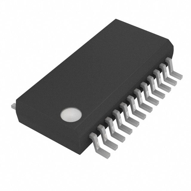
| 描述 | IC 4INPUT 12BIT ADC 24-QSOP模数转换器 - ADC Dual 500kHz 2+2 Ch Simltns Smplng ADC |
| 产品分类 | |
| 品牌 | Texas Instruments |
| 产品手册 | |
| 产品图片 |
|
| rohs | 符合RoHS无铅 / 符合限制有害物质指令(RoHS)规范要求 |
| 产品系列 | 数据转换器IC,模数转换器 - ADC,Texas Instruments ADS7861EBG4- |
| 数据手册 | |
| 产品型号 | ADS7861EBG4 |
| 产品培训模块 | http://www.digikey.cn/PTM/IndividualPTM.page?site=cn&lang=zhs&ptm=13240 |
| 产品种类 | 模数转换器 - ADC |
| 位数 | 12 |
| 供应商器件封装 | 24-SSOP/QSOP |
| 信噪比 | 71 dB |
| 分辨率 | 12 bit |
| 制造商产品页 | http://www.ti.com/general/docs/suppproductinfo.tsp?distId=10&orderablePartNumber=ADS7861EBG4 |
| 包装 | 管件 |
| 单位重量 | 129.500 mg |
| 商标 | Texas Instruments |
| 安装类型 | 表面贴装 |
| 安装风格 | SMD/SMT |
| 封装 | Tube |
| 封装/外壳 | 24-SSOP(0.154",3.90mm 宽) |
| 封装/箱体 | SSOP-24 |
| 工作温度 | -40°C ~ 125°C |
| 工作电源电压 | 5 V |
| 工厂包装数量 | 50 |
| 接口类型 | Serial, SPI |
| 数据接口 | 串行 |
| 最大功率耗散 | 42.5 mW |
| 最大工作温度 | + 125 C |
| 最小工作温度 | - 40 C |
| 标准包装 | 50 |
| 电压参考 | Internal, External |
| 电压源 | 模拟和数字 |
| 系列 | ADS7861 |
| 结构 | SAR |
| 转换器数 | 2 |
| 转换器数量 | 2 |
| 转换速率 | 500 kS/s |
| 输入数和类型 | 8 个单端,双极4 个差分,双极 |
| 输入类型 | Differential |
| 通道数量 | 4 Channel |
| 配用 | /product-detail/zh/ADS7861EVM/296-19915-ND/562122 |
| 采样率(每秒) | 500k |


- 商务部:美国ITC正式对集成电路等产品启动337调查
- 曝三星4nm工艺存在良率问题 高通将骁龙8 Gen1或转产台积电
- 太阳诱电将投资9.5亿元在常州建新厂生产MLCC 预计2023年完工
- 英特尔发布欧洲新工厂建设计划 深化IDM 2.0 战略
- 台积电先进制程称霸业界 有大客户加持明年业绩稳了
- 达到5530亿美元!SIA预计今年全球半导体销售额将创下新高
- 英特尔拟将自动驾驶子公司Mobileye上市 估值或超500亿美元
- 三星加码芯片和SET,合并消费电子和移动部门,撤换高东真等 CEO
- 三星电子宣布重大人事变动 还合并消费电子和移动部门
- 海关总署:前11个月进口集成电路产品价值2.52万亿元 增长14.8%


PDF Datasheet 数据手册内容提取
ADS7861 ADS7861 ADS7861 SBAS110D – DECEMBER 1998 – REVISED AUGUST 2007 Dual, 500kSPS, 12-Bit, 2 + 2 Channel, Simultaneous Sampling ANALOG-TO-DIGITAL CONVERTER FEATURES DESCRIPTION (cid:1) 4 INPUT CHANNELS The ADS7861 is a dual, 12-bit, 500kSPS, Analog-to-Digital (cid:1) FULLY DIFFERENTIAL INPUTS (A/D) converter with four fully differential input channels (cid:1) 2µs TOTAL THROUGHPUT PER CHANNEL grouped into two pairs for high speed, simultaneous signal acquisition. Inputs to the sample-and-hold amplifiers are fully (cid:1) NO MISSING CODES differential and are maintained differential to the input of the (cid:1) 1MHz EFFECTIVE SAMPLING RATE A/D converter. This provides excellent common-mode rejec- (cid:1) LOW POWER: 40mW tion of 80dB at 50kHz which is important in high noise (cid:1) SSI SERIAL INTERFACE environments. (cid:1) OPERATING TEMPERATURE RANGE: The ADS7861 offers a high-speed, dual serial interface and ° ° –40 C to +125 C control inputs to minimize software overhead. The output data for each channel is available as a 12-bit word. The ADS7861 APPLICATIONS is offered in both an SSOP-24 and a QFN-32 package and is fully specified over the –40°C to +125°C operating range. (cid:1) MOTOR CONTROL (cid:1) MULTI-AXIS POSITIONING SYSTEMS (cid:1) 3-PHASE POWER CONTROL CH A0+ SAR CH A0– SHA COMP CDAC SERIAL DATA A CH A1+ SERIAL DATA B CH A1– M0 M1 REFIN Serial A0 Internal REFOUT 2.5V Interface CLOCK Reference CS CH B0+ RD CH B0– SHA COMP BUSY CDAC CONVST CH B1+ CH B1– SAR Please be aware that an important notice concerning availability, standard warranty, and use in critical applications of Texas Instruments semiconductor products and disclaimers thereto appears at the end of this data sheet. All trademarks are the property of their respective owners. PRODUCTION DATA information is current as of publication date. Copyright © 1998-2007, Texas Instruments Incorporated Products conform to specifications per the terms of Texas Instruments standard warranty. Production processing does not necessarily include testing of all parameters. www.ti.com
ABSOLUTE MAXIMUM RATINGS(1) ELECTROSTATIC DISCHARGE SENSITIVITY Analog Inputs to AGND, Any Channel Input........–0.3V to (+V + 0.3V) D REF .....................................................................–0.3V to (+V + 0.3V) IN D Digital Inputs to DGND..........................................–0.3V to (+VD + 0.3V) This integrated circuit can be damaged by ESD. Texas Instruments Ground Voltage Differences: AGND, DGND...................................±0.3V recommends that all integrated circuits be handled with appropriate +V to AGND.........................–0.3V to +6V D precautions. Failure to observe proper handling and installation proce- Power Dissipation..........................................................................325mW Maximum Junction Temperature...................................................+150°C dures can cause damage. Operating Temperature Range......................................–40°C to +125°C Storage Temperature Range.........................................–65°C to +150°C ESD damage can range from subtle performance degradation to complete device failure. Precision integrated circuits may be more NOTE: (1) Stresses above these ratings may cause permanent damage. susceptible to damage because very small parametric changes could Exposure to absolute maximum conditions for extended periods may degrade cause the device not to meet its published specifications. device reliability. PACKAGE/ORDERING INFORMATION For the most current package and ordering information, see the Package Option Addendum at the end of this document, or see the TI website at www.ti.com. TRUTH TABLE M0 M1 A0 TWO-CHANNEL/FOUR-CHANNEL OPERATION DATA ON SERIAL OUTPUTS CHANNELS CONVERTED 0 0 0 Two Channel A and B A0, B0 0 0 1 Two Channel A and B A1, B1 0 1 0 Two Channel A Only A0, B0 0 1 1 Two Channel A Only A1, B1 1 0 X Four Channel A and B Sequential 1 1 X Four Channel A Only Sequential X = Don’t Care. BASIC CIRCUIT CONFIGURATION ADS7861 1 DGND +V 24 D 2 CH B1+ SERIAL DATA A 23 3 CH B1– SERIAL DATA B 22 4 CH B0+ BUSY 21 BUSY Output 5 CH B0– CLOCK 20 Clock Input 6 CH A1+ CS 19 Chip Select 7 CH A1– RD 18 Read Input 8 CH A0+ CONVST 17 Conversion Start 9 CH A0– A0 16 A0 Address Select 10 REF M0 15 M0 Address Select IN 11 REF M1 14 M1 Address Select OUT 12 AGND +V 13 +5V Analog Supply A + + 10µF 0.1µF ADS7861 2 SBAS110D
ELECTRICAL CHARACTERISTICS Over recommended operating free-air temperature range at T = –40°C to +125°C, +V + V = +5V, V = internal +2.5V, f = 8MHz, and f = 500kSPS, A A D REF CLK SAMPLE unless otherwise noted. ADS7861I, E ADS7861IB, EB PARAMETER CONDITIONS MIN TYP MAX MIN TYP MAX UNITS RESOLUTION 12 ✻ Bits ANALOG INPUT Input Voltage Range-Bipolar V = Internal V at 2.5V –V +V ✻ ✻ V CENTER REF REF REF Input Capacitance 15 ✻ pF Input Leakage Current ±1 ✻ µA SYSTEM PERFORMANCE No Missing Codes 12 ✻ Bits Integral Linearity ±0.75 ±2 ±0.5 ±1 LSB Integral Linearity Match 0.5 ±1 ✻ ✻ LSB Differential Linearity ±1 ±0.5 ±1 LSB Bipolar Offset Error T = –40°C to +85°C ±0.5 ±3 ✻ ✻ LSB A T = –40°C to +125°C ±0.5 ±3.5 ✻ ✻ LSB A Bipolar Offset Error Match 3 2 LSB Positive Gain Error Referenced to REF ±0.15 ±0.75 ±0.10 ±0.50 % of FSR IN Positive Gain Error Match 2 1 LSB Negative Gain Error Referenced to REF ±0.15 ±0.75 ±0.10 ±0.50 % of FSR IN Negative Gain Error Match 2 1 LSB Common-Mode Rejection Ratio At DC 80 ✻ dB V = ±1.25V at 50kHz 80 ✻ dB IN PP Noise 120 ✻ µVrms Power Supply Rejection Ratio 0.5 2 ✻ ✻ LSB SAMPLING DYNAMICS Conversion Time per A/D 1.625 ✻ µs Acquisition Time 0.375 ✻ µs Throughput Rate 500 ✻ kSPS Aperture Delay 3.5 ✻ ns Aperture Delay Matching 100 ✻ ps Aperture Jitter 50 ✻ ps Small-Signal Bandwidth 40 ✻ MHz DYNAMIC CHARACTERISTICS (V = ±2.5V at 100kHz) IN PP Total Harmonic Distortion T = –40°C to +85°C –72 –76 dB A T = –40°C to +125°C –71 –75 dB A SINAD 70 ✻ dB Spurious Free Dynamic Range T = –40°C to +85°C 72 76 dB A T = –40°C to +125°C 71 75 dB A Channel-to-Channel Isolation –80 ✻ dB VOLTAGE REFERENCE Internal 2.475 2.5 2.525 ✻ ✻ ✻ V Internal Drift ±25 ✻ ppm/°C Internal Noise 50 ✻ µV PP Internal Source Current 2 ✻ mA Internal Load Rejection 0.005 ✻ mV/µA Internal PSRR 80 ✻ dB External Voltage Range 1.2 2.5 2.6 ✻ ✻ ✻ V Input Current 0.05 1 ✻ ✻ µA Input Capacitance 5 ✻ pF DIGITAL INPUT/OUTPUT Logic Family CMOS ✻ Logic Levels: V I = +5µA 3.0 +V + 0.3 ✻ ✻ V IH IH DD V I = +5µA –0.3 1 ✻ ✻ V IL IL V I = –0.5mA 3.5 ✻ V OH OH V I = –0.5mA 0.4 ✻ V OL OL External Clock, Optional 0.2 8 ✻ ✻ MHz Data Format Binary Two's Complement ✻ POWER SUPPLY REQUIREMENTS Power Supply Voltage, +V 4.75 5 5.25 ✻ ✻ ✻ V Quiescent Current, +V T = –40°C to +85°C 5 8 ✻ ✻ mA A A T = –40°C to +125°C 5 8.5 ✻ ✻ mA A Power Dissipation T = –40°C to +85°C 25 40 ✻ ✻ mW A T = –40°C to +125°C 25 42.5 ✻ ✻ mW A ✻ Specifications same as ADS7861I, ADS7861E. ADS7861 3 SBAS110D
PIN CONFIGURATIONS Top View SSOP Top View A QFN ADS7861 TA A D D AL 1 DGND +VD 24 (2)NC (2)NC (2)NC (2)NC DGN +VD (2)NC SERI 2 CH B1+ SERIAL DATA A 23 32 31 30 29 28 27 26 25 3 CH B1– SERIAL DATA B 22 CH B1+ 1 24 SERIAL DATA B 4 CH B0+ BUSY 21 CH B1− 2 23 BUSY 5 CH B0– CLOCK 20 CH B0+ 3 22 CLOCK CH B0− 4 21 CS 6 CH A1+ CS 19 ADS7861(1) CH A1+ 5 20 RD 7 CH A1– RD 18 CH A1− 6 19 CONVST CH A0+ 7 18 A0 8 CH A0+ CONVST 17 CH A0− 8 17 M0 9 CH A0– A0 16 10 REF M0 15 9 10 11 12 13 14 15 16 11 REFIONUT M1 14 REFIN REFOUT (2)NC AGND +VA (2)NC (2)NC M1 12 AGND +V 13 A NOTE: (1)The thermal pad is internally connected to the substrate. This pad can be connected to the analog ground or left floating. Keep the thermal pad separate from the digital ground, if possible. (2)NC = Not Connected. PIN DESCRIPTIONS SSOP QFN PIN PIN NAME DESCRIPTION 1 28 DGND Digital Ground. Connect directly to analog ground (pin 12). 2 1 CH B1+ Noninverting Input Channel B1 3 2 CH B1– Inverting Input Channel B1 4 3 CH B0+ Noninverting Input Channel B0 5 4 CH B0– Inverting Input Channel B0 6 5 CH A1+ Noninverting Input Channel A1 7 6 CH A1– Inverting Input Channel A1 8 7 CH A0+ Noninverting Input Channel A0 9 8 CH A0– Inverting Input Channel A0 10 9 REF Reference Input IN 11 10 REF 2.5V Reference Output OUT 12 12 AGND Analog Ground. Connect directly to digital ground (pin 1). 13 13 +V Analog Power Supply, +5VDC. Connect directly to digital power supply (pin 24). Decouple to analog ground with a 0.1µF ceramic capacitor A and a 10µF tantalum capacitor. 14 16 M1 Selects between the Serial Outputs. When M1 is LOW, both Serial Output A and Serial Output B are selected for data transfer. When M1 is HIGH, Serial output A is configured for both Channel A data and Channel B data; Serial Output B goes into tri-state (i.e., high impedance). 15 17 M0 Selects between two-channel and four-channel operation. When M0 is LOW, two-channel operation is selected and operates in conjunction with A0. When A0 is HIGH, Channel A1 and Channel B1 are being converted. When A0 is LOW, Channel A0 and Channel B0 are being converted. When M0 is HIGH, four-channel operation is selected. In this mode, all four channels are converted in sequence starting with Channels A0 and B0, followed by Channels A1 and B1. 16 18 A0 A0 operates in conjunction with M0. With M0 LOW and A0 HIGH, Channel A1 and Channel B1 are converted. With M0 LOW and A0 LOW, Channel A0 and Channel B0 are converted. 17 19 CONVST Convert Start. When CONVST switches from LOW to HIGH, the device switches from the sample to hold mode, independent of the status of the external clock. 18 20 RD Synchronization Pulse for the Serial Output. 19 21 CS Chip Select. When LOW, the Serial Output A and Serial Output B outputs are active; when HIGH, the serial outputs are tri-stated. 20 22 CLOCK An external CMOS-compatible clock can be applied to the CLOCK input to synchronize the conversion process to an external source. The CLOCK pin controls the sampling rate by the equation: CLOCK = 16 • f . SAMPLE 21 23 BUSY BUSY goes HIGH during a conversion and returns LOW after the third LSB has been transmitted on either the Serial A or Serial B output pin. 22 24 SERIAL The Serial Output data word is comprised of channel information and 12 bits of data. In operation, data is valid on the falling edge of DATA B DCLOCK for 16 edges after the rising edge of RD. 23 25 SERIAL The Serial Output data word is comprised of channel information and 12 bits of data. In operation, data is valid on the falling edge of DATA A DCLOCK for 16 edges after the rising edge of RD. When M1 is HIGH, both Channel A data and Channel B data are available. 24 27 +V Digital Power Supply, +5VDC. Connect directly to pin 13. Must be ≤ +V . D A ADS7861 4 SBAS110D
TYPICAL CHARACTERISTICS At T = +25°C, +V + V = +5V, and V = internal +2.5V, f = 8MHz, f = 500kSPS, unless otherwise noted. A A D REF CLK SAMPLE FREQUENCY SPECTRUM FREQUENCY SPECTRUM (4096 Point FFT; f = 99.9kHz, –0.5dB) (4096 Point FFT; f = 199.9kHz, –0.5dB) IN IN 0 0 –20 –20 B) –40 B) –40 d d e ( e ( ud –60 ud –60 plit plit m m A –80 A –80 –100 –100 –120 –120 0 62.5 125 187.5 250 0 62.5 125 187.5 250 Frequency (kHz) Frequency (kHz) SIGNAL-TO-NOISE RATIO and CHANGE IN SIGNAL-TO-NOISE RATIO SIGNAL-TO-(NOISE+DISTORTION) AND SIGNAL-TO-(NOISE+DISTORTION) vs INPUT FREQUENCY vs TEMPERATURE 76 0.7 0.6 74 SNR B) dB) 0.5 SINAD (d 7720 SINAD °m +25C ( 00..43 d o SNR an 68 Delta fr 00..21 SNR SINAD 66 0 64 –0.1 1k 10k 100k 1M –40 25 85 Input Frequency (Hz) Temperature (°C) CHANGE IN SPURIOUS FREE DYNAMIC RANGE CHANGE IN POSITIVE GAIN MATCH AND TOTAL HARMONIC DISTORTION vs TEMPERATURE vs TEMPERATURE (Maximum Deviation for All Four Channels) 7 +1 0.6 B) 6 0 S °m +25C (dB) 54 THD ––01.5 °m +25C (dB) Gain Match (L 00..54 SFDR Delta fro 321 SFDR –––122..55 THD Delta fro nge in Positive 000...321 0 –3 a h C –1 –3.5 0 –40 25 85 –40 25 85 150 Temperature (°C) Temperature (°C) ADS7861 5 SBAS110D
TYPICAL CHARACTERISTICS (Cont.) At T = +25°C, +V + V = +5V, and V = internal +2.5V, f = 8MHz, f = 500kSPS, unless otherwise noted. A A D REF CLK SAMPLE CHANGE IN NEGATIVE GAIN MATCH vs TEMPERATURE CHANGE IN REFERENCE VOLTAGE (Maximum Deviation for All Four Channels) vs TEMPERATURE 0.2 2.51 B) S 0.18 L ch ( 0.16 V) 2.505 Mat 0.14 ce ( gative Gain 00.0.10.128 e in Referen 2.429.55 e g e in N 00..0064 Chan 2.49 g n a 0.02 h C 0 2.485 –40 25 85 150 –40 25 85 150 Temperature (°C) Temperature (°C) CHANGE IN BIPOLAR ZERO vs TEMPERATURE CHANGE IN BPZ MATCH vs TEMPERATURE 0.75 1 ero (LSB) 0.02.55 B Channel atch (LSB) 0.75 Z M Change in Bipolar –0–.02.550 A Channel Change in Bipolar 00.2.55 –0.75 0 –40 25 85 150 –40 25 85 150 Temperature (°C) Temperature (°C) CHANGE IN CMRR vs TEMPERATURE INTEGRAL LINEARITY ERROR vs CODE 86 1 Typical of All Four Channels 85 0.75 B) 84 0.5 d RR ( 83 B) 0.25 M S ge in C 8821 ILE (L –0.205 n a Ch 80 –0.5 79 –0.75 78 –1 –40 –5 25 55 85 800 000 7FF Temperature (°C) Hex BTC Code ADS7861 6 SBAS110D
TYPICAL CHARACTERISTICS (Cont.) At T = +25°C, +V + V = +5V, and V = internal +2.5V, f = 8MHz, f = 500kSPS, unless otherwise noted. A A D REF CLK SAMPLE DIFFERENTIAL LINEARITY ERROR vs CODE INTEGRAL LINEARITY ERROR vs TEMPERATURE 1 0.8 Typical of All Four Channels 0.75 0.7 Positive ILE 0.5 0.6 B) S 0.4 E (LSB) 0.250 n ILE (L 0.2 DL –0.25 ge i 0 an –0.2 h –0.5 C –0.4 Negative ILE –0.75 –0.6 –1 –0.8 800 000 7FF –40 25 85 150 Hex BTC Code Temperature (°C) INTEGRAL LINEARITY ERROR MATCH DIFFERENTIAL LINEARITY ERROR vs CODE CHANNEL A0/CHANNEL A1 vs TEMPERATURE (Same Converter, Different Channels) 0.8 0.25 Positive DLE 0.6 0.2 0.15 0.4 B) 0.1 S 0.2 Error (L 0 E (LSB) 0.050 LE –0.2 IL –0.05 D Negative DLE –0.1 –0.4 –0.15 –0.6 –0.2 –0.8 –0.25 –40 25 85 150 800 000 7FF Temperature (°C) Hex BTC Code INTEGRAL LINEARITY ERROR MATCH INTEGRAL LINEARITY ERROR MATCH vs TEMPERATURE vs CODE CHANNEL A0/CHANNEL B1 Channel A0/Channel B0 (Different Converter, Different Channels) (Different Converter, Different Channels) 0.25 0.47 0.2 0.46 0.15 SB) 0.45 0.1 h (L 0.44 B) 0.05 atc S M 0.43 ILE (L –0–.00.051 ge in INL 00..4421 n –0.15 ha 0.40 C –0.2 0.39 –0.25 0.38 800 000 7FF –40 25 85 150 Hex BTC Code Temperature (°C) ADS7861 7 SBAS110D
INTRODUCTION REFERENCE Under normal operation, the REF pin should be directly The ADS7861 is a high-speed, low power, dual, 12-bit A/D OUT connected to the REF pin to provide an internal +2.5V converter that operates from a single +5V supply. The input IN reference to the ADS7861. The ADS7861 can operate, channels are fully differential with a typical common-mode however, with an external reference in the range of 1.2V to rejection of 80dB. The part contains dual, 2µs successive 2.6V for a corresponding full-scale range of 2.4V to 5.2V. approximation ADCs, two differential sample-and-hold am- plifiers, an internal +2.5V reference with REF and REF The internal reference of the ADS7861 is double-buffered. IN OUT pins and a high-speed parallel interface. The ADS7861 If the internal reference is used to drive an external load, a requires an external clock. In order to achieve the maximum buffer is provided between the reference and the load ap- throughput rate of 500kSPS, the master clock must be set at plied to pin 2 (the internal reference can typically source 8MHz. A minimum of 16 clock cycles are required for each 2mA of current load—capacitance should not exceed 100pF). 12-bit conversion. If an external reference is used, the second buffer provides isolation between the external reference and the CDAC. There are four analog inputs that are grouped into two chan- This buffer is also used to recharge all of the capacitors of nels (A and B). Channel selection is controlled by the M0, M1 both CDACs during conversion. and A0 pins. Each channel has two inputs (A0 and A1 and B0 and B1) that can be sampled and converted simultaneously, ANALOG INPUT thus preserving the relative phase information of the signals on both analog inputs. The part accepts an analog input voltage in The analog input is bipolar and fully differential. There are the range of –V to +V , centered around the internal two general methods of driving the analog input of the REF REF +2.5V reference. The part will also accept bipolar input ranges ADS7861: single-ended or differential (see Figures 1 and 2). when a level shift circuit is used at the front end (see Figure 7). When the input is single-ended, the –IN input is held at the common-mode voltage. The +IN input swings around the All conversions are initiated on the ADS7861 by bringing same common voltage and the peak-to-peak amplitude is the the CONVST pin HIGH for a minimum of 15ns. CONVST (common-mode +V ) and the (common-mode –V ). HIGH places both sample-and-hold amplifiers in the hold REF REF The value of V determines the range over which the state simultaneously and the conversion process is started on REF common-mode voltage may vary (see Figure 3). both channels. The RD pin can be connected to CONVST to simplify operation. Depending on the status of the M0, M1 When the input is differential, the amplitude of the input is the and A0 pins, the ADS7861 will (a) operate in either two- difference between the +IN and –IN input, or (+IN) – (–IN). channel or four-channel mode and (b) output data on both The peak-to-peak amplitude of each input is ±1/2V around REF the Serial A and Serial B output or both channels can be this common voltage. However, since the inputs are 180° out transmitted on the A output only. of phase, the peak-to-peak amplitude of the differential volt- age is +V to –V . The value of V also determines the NOTE: See the Timing and Control section of this data sheet REF REF REF range of the voltage that may be common to both inputs (see for more information. Figure 4). SAMPLE-AND-HOLD SECTION The sample-and-hold amplifiers on the ADS7861 allow the ADCs to accurately convert an input sine wave of full-scale amplitude to 12-bit accuracy. The input bandwidth of the sample-and-hold is greater than the Nyquist rate (Nyquist –V to +V REF REF ADS7861 equals one-half of the sampling rate) of the ADC even when peak-to-peak the ADC is operated at its maximum throughput rate of Common 500kSPS. The typical small-signal bandwidth of the sample- Voltage and-hold amplifiers is 40MHz. Single-Ended Input Typical aperture delay time or the time it takes for the ADS7861 to switch from the sample to the hold mode V following the CONVST pulse is 3.5ns. The average delta of REF peak-to-peak repeated aperture delay values is typically 50ps (also known ADS7861 Common V as aperture jitter). These specifications reflect the ability of REF Voltage peak-to-peak the ADS7861 to capture AC input signals accurately at the exact same moment in time. Differential Input FIGURE 1. Methods of Driving the ADS7861 Single-Ended or Differential. ADS7861 8 SBAS110D
CM+V +IN REF +V REF CMVoltage –IN = CM Voltage –V REF CM–V t REF Single-Ended Inputs +IN CM+1/2V REF +V REF CMVoltage –V REF –IN CM–1/2V t REF Differential Inputs (IN+) + (IN–) NOTES: Common-Mode Voltage (Differential Mode) = Common-Mode Voltage (Single-Ended Mode) = IN–. 2 The maximum differential voltage between +IN and –IN of the ADS7861 is V . See Figures 3 and 4 for a further REF explanation of the common voltage range for single-ended and differential inputs. FIGURE 2. Using the ADS7861 in the Single-Ended and Differential Input Modes. 5 5 4.7 VCC = 5V VCC = 5V 4.1 4 4 4.0 V) V) ge ( 3 Single-Ended Input 2.7 ge ( 3 Differential Input n n a a R R ge 2 2.3 ge 2 a a olt olt V V on 1 on 1 1.0 m 0.9 m m m o o C C 0.3 0 0 –1 –1 1.2 2.6 1.2 2.6 1.0 1.5 2.0 2.5 3.0 1.0 1.5 2.0 2.5 3.0 VREF (V) VREF (V) FIGURE 3. Single-Ended Input: Common-Mode Voltage FIGURE 4. Differential Input: Common-Mode Voltage Range vs V . Range vs V . REF REF In each case, care should be taken to ensure that the output capacitance has been fully charged, there is no further input impedance of the sources driving the +IN and –IN inputs are current. The source of the analog input voltage must be able matched. Otherwise, this may result in offset error, gain to charge the input capacitance (15pF) to a 12-bit settling error and linearity error which will change with both tem- level within 2 clock cycles. When the converter goes into the perature and input voltage. hold mode, the input impedance is greater than 1GΩ. The input current on the analog inputs depend on a number Care must be taken regarding the absolute analog input of factors: sample rate, input voltage, and source impedance. voltage. The +IN input should always remain within the Essentially, the current into the ADS7861 charges the inter- range of GND – 300mV to V + 0.3V. DD nal capacitor array during the sampling period. After this ADS7861 9 SBAS110D
TRANSITION NOISE DESCRIPTION ANALOG INPUT Figure 5 shows a histogram plot for the ADS7861 following Full-Scale Input Span –V to +V (1) DIGITAL OUTPUT REF REF 8,000 conversions of a DC input. The DC input was set at BINARY TWO’S COMPLEMENT Least Significant (–V to +V )/4096(2) REF REF output code 2046. All but one of the conversions had an Bit (LSB) BINARY CODE HEX CODE output code result of 2046 (one of the conversions resulted +Full Scale 4.99878V 0111 1111 1111 7FF in an output of 2047). The histogram reveals the excellent Midscale 2.5V 0000 0000 0000 000 noise performance of the ADS7861. Midscale – 1 LSB 2.49878V 1111 1111 1111 FFF –Full Scale 0V 1000 0000 0000 800 BIPOLAR INPUTS NOTES: (1) –VREF to +VREF around VREF. With a 2.5V reference, this corre- sponds to a 0V to 5V input span. (2) 1.22mV with a 2.5V reference. The differential inputs of the ADS7861 were designed to TABLE I. Ideal Input Voltages and Output Codes. accept bipolar inputs (–V and +V ) around the internal REF REF reference voltage (2.5V), which corresponds to a 0V to 5V input range with a 2.5V reference. By using a simple op amp TIMING AND CONTROL circuit featuring a single amplifier and four external resis- The operation of the ADS7861 can be configured in four tors, the ADS7861 can be configured to except bipolar different modes by using the address pins M0, M1 and A0. inputs. The conventional ±2.5V, ±5V, and ±10V input The M0 pin selects between two- and four-channel operation ranges can be interfaced to the ADS7861 using the resistor (in two-channel operation, the A0 pin selects between Chan- values shown in Figure 7. nels 0 and 1; in four-channel operation the A0 pin is ignored and the channels are switched automatically after each conversion). The M1 pin selects between having serial data transmitted simultaneously on both the Serial A data output 8000 and the Serial B data output or having both channels output data through the Serial A port. The A0 pin selects either 7000 Channel 0 or Channel 1 (see Pin Descriptions and Serial s on 6000 Output Truth Table for more information). si ver 5000 The next four sections will explain the four different modes n o C 4000 of operation. of er 3000 Mode I (M0 = 0, M1 = 0) b m With the M0 and M1 pins both set to ‘0’, the ADS7861 will Nu 2000 operate in two-channel operation (the A0 pin must be used 1000 to switch between Channels A and B). A conversion is 0 initiated by bringing CONVST HIGH for a minimum of 2044 2045 2046 2047 2048 15ns. It is very important that CONVST be brought HIGH Code (decimal) a minimum of 10ns prior to a rising edge of the external clock or 5ns after the rising edge. If CONVST is brought FIGURE 5. Histogram of 8,000 Conversions of a DC Input. R 1 1.4V 4kΩ 3kΩ 20kΩ OPA132 +IN Bipolar Input –IN DATA Test Point ADS7861 100pF R C 2 LOAD REF OUT 2.5V DATA VOH BIPOLAR INPUT R1 R2 V ±10V 1kΩ 5kΩ OL ±5V 2kΩ 10kΩ tR tF ±2.5V 4kΩ 20kΩ Voltage Waveforms for DATA Rise and Fall Times t , and t . R F FIGURE 7. Level Shift Circuit for Bipolar Input Ranges. FIGURE 6. Test Circuits for Timing Specifications. ADS7861 10 SBAS110D
HIGH within this window, it is then uncertain as to when the Channel 1, LOW = Channel 0). The address must be selected ADS7861 will initiate conversion (see Figure 8 for a more 15ns prior to the falling edge of cycle one of the external clock detailed description). Sixteen clock cycles are required to and must remain ‘held’ for 15ns following the clock edge. For perform a single conversion. Immediately following maximum throughput time, the CONVST and RD pins should CONVST switching to HIGH, the ADS7861 will switch be tied together. CS must be brought LOW to enable the two from the sample mode to the hold mode asynchronous to the serial outputs. Data will be valid on the falling edge of all 16 external clock. The BUSY output pin will then go HIGH and clock cycles per conversion. The first bit of data will be a remain HIGH for the duration of the conversion cycle. On status flag for either Channel 0 or 1, the second bit will be a the falling edge of the first cycle of the external clock, the second status flag for either Channel A or B. The subsequent ADS7861 will latch in the address for the next conversion data will be MSB-first through the LSB, followed by two cycle depending on the status of the A0 pin (HIGH = zeros (see Table II and Figures 9 and 10). t CKP 125ns CLOCK Cycle 1 Cycle 2 10ns 10ns 5ns 5ns CONVST A B C NOTE: All CONVST commands which occur more than 10ns before the rising edge of cycle ‘1’ of the external clock (Region ‘A’) will initiate a conversion on the rising edge of cycle ‘1’. All CONVST commands which occur 5ns after the rising edge of cycle ‘1’ or 10ns before the rising edge of cycle 2 (Region ‘B’) will initiate a conversion on the rising edge of cycle ‘2’. All CONVST commands which occur 5ns after the rising edge of cycle ‘2’ (Region ‘C’) will initiate a conversion on the rising edge of the next clock period. The CONVST pin should never be switched from LOW to HIGH in the region 10ns prior to the rising edge of the CLOCK and 5ns after the rising edge (gray areas). If CONVST is toggled in this gray area, the conversion could begin on either the same rising edge of the CLOCK or the following edge. FIGURE 8. Conversion Mode. TIMING SPECIFICATIONS SYMBOL DESCRIPTION MIN TYP MAX UNITS COMMENTS t Conversion Time 1.75 µs When T = 125ns CONV CKP t Acquisition Time 0.25 µs When T = 125ns ACQ CKP t Clock Period 125 5000 ns CKP t Clock LOW 40 ns CKL t Clock HIGH 40 ns CKH t DOUT Fall Time 25 ns F t DOUT Rise Time 30 ns R t CONVST HIGH 15 ns 1 t Address Setup Time 15 ns Address latched on falling edge of CLK cycle ‘2’ 2 t Address Hold Time 15 3 t RD Setup Time 15 ns Before falling edge of CLOCK 4 t RD to CS Hold Time 15 ns After falling edge of CLOCK 5 t CONVST LOW 20 ns 6 t RD LOW 20 ns 7 t CS to Data Valid 25 ns 8 t CLOCK to Data Valid Delay 30 ns Maximum delay following rising edge of CLOCK 9 t Data Valid After CLOCK(1) 1 ns Time data is valid after second rising edge of CLOCK 10 NOTE: (1) ‘n – 1’ data will remain valid 1ns after rising edge of next CLOCK cycle. CLOCK CYCLE 1 2 3 4 5 6 7 8 9 10 11 12 13 14 15 16 SERIAL DATA CH0 OR CH1 CHA OR CHB DB11 DB10 DB9 DB8 DB7 DB6 DB5 DB4 DB3 DB2 DB1 DB0 0 0 TABLE II. Serial Data Output Format. ADS7861 11 SBAS110D
Mode II (M0 = 0, M1 = 1) The basic SAR architecture is sensitive to glitches or sudden With M1 set to ‘1’, the ADS7861 will output data on the changes on the power supply, reference, ground connections Serial Data A pin only. All other pins function in the same and digital inputs that occur just prior to latching the output manner as Mode I except that the Serial Data B output will of the analog comparator. Thus, driving any single conver- tri-state (i.e., high impedance) after a conversion following sion for an n-bit SAR converter, there are n “windows” in M1 going HIGH. Another difference in this mode involves which large external transient voltages can affect the conver- the CONVST pin. Since it takes 32 clock cycles to output sion result. Such glitches might originate from switching the results from both A/D converters (rather than 16 when power supplies, nearby digital logic or high power devices. M1 = 0), the ADS7861 will take 4µs to complete a The degree of error in the digital output depends on the conversion on both A/Ds (See Figure 11). reference voltage, layout, and the exact timing of the exter- nal event. Their error can change if the external event Mode III (M0 = 1, M1 = 0) changes in time with respect to the CLOCK input. With M0 set to ‘1’, the ADS7861 will cycle through Chan- With this in mind, power to the ADS7861 should be clean nels 0 and 1 sequentially (the A0 pin is ignored). At the same and well-bypassed. A 0.1µF ceramic bypass capacitor should time, setting M1 to ‘0’ places both Serial Outputs, A and B, be placed as close to the device as possible. In addition, a in the active mode (See Figure 12). 1µF to 10µF capacitor is recommended. If needed, an even Mode IV (M0 = 1, M1 = 1) larger capacitor and a 5Ω or 10Ω series resistor may be used Similar to Mode II, Mode IV uses the Serial A output line to to low pass filter a noisy supply. On average, the ADS7861 transmit data exclusively. Following the first conversion draws very little current from an external reference as the after M1 goes HIGH, the serial B output will go into tri- reference voltage is internally buffered. However, glitches state. See Figure 13. As in Mode II, the second CONVST from the conversion process appear at the V input and the REF command is always ignored when M1 = 1. reference source must be able to handle this. Whether the reference is internal or external, the V pin should be REF bypassed with a 0.1µF capacitor. An additional larger ca- READING DATA pacitor may also be used, if desired. If the reference voltage In all four timing diagrams, the CONVST pin and the RD is external and originates from an op amp, make sure that it pins are tied together. If so desired, the two lines can be can drive the bypass capacitor or capacitors without oscilla- separated. Data on the Serial Output pins (A and B) will tion. No bypass capacitor is necessary when using the become valid following the third rising SCLK edge follow- internal reference (tie pin 10 directly to pin 11). ing RD rising edge. Refer to Table II for data output format. The GND pin should be connected to a clean ground point. In many cases, this will be the ‘analog’ ground. Avoid LAYOUT connections which are too near the grounding point of a microcontroller or digital signal processor. If required, run a For optimum performance, care should be taken with the ground trace directly from the converter to the power supply physical layout of the ADS7861 circuitry. This is particu- entry point. The ideal layout will include an analog ground larly true if the CLOCK input is approaching the maximum plane dedicated to the converter and associated analog throughput rate. circuitry. ADS7861 12 SBAS110D
Conversion 1 Start of Conversion 2 tCKH CLOCK 0 1 2 3 4 5 6 7 8 9 10 11 12 13 14 15 16 1 2 3 4 5 6 tCKL t6 CONVST t1 t2 t3 A0 t4 t5 RD t7 CS SERIAL t8 t9 t10 DATA A 0 0 D11 D10 D9 D8 D7 D6 D5 D4 D3 D2 D1 D0 0 0 0 0 D11 D10 D9 D8 SERIAL DATA B 0 0 D11 D10 D9 D8 D7 D6 D5 D4 D3 D2 D1 D0 0 0 0 0 D11 D10 D9 D8 BUSY tCONV tACQ tCONV FIGURE 9. Mode I with Timing Specifications. 1 16 CLOCK CONVST Conversion of Ch1 Conversion of Ch0 A0 A0 HIGH, Next Conversion: Ch1 A0 LOW, Next Conversion: Ch0 RD Connected to CONVST RD CS CS HIGH, Outputs in Tri-State SERIAL DATA A 12-Bit Data of Chx 12-Bit Data of ChA1 SERIAL 12-Bit Data of Chx 12-Bit Data of ChB1 DATA B BUSY Conversion of Chx Conversion of Ch1 Conversion of Ch0 TIME 0 1µs 2µs 3µs 4µs 5µs 6µs Time (seconds) FIGURE 10. Mode I, Timing Diagram for M0 = 0 and M1 = 0. ADS7861 13 SBAS110D
1 16 CLOCK M1 = 1 and 1st CONVST M1 = 1 and 2nd CONVST M1 = 1 and 1st CONVST M1 = 1 and 2nd CONVST CONVST Conversion of Chx Conversion No Conversion Conversion No Conversion A0 HIGH A0 LOW A0 LOW A0 Next Conversion Ch1 Next Conversion Ch0 Next Conversion Ch0 M1 HIGH M1 Only Serial Data A Used as Output Starting with 1st Conversion RD RD Connected with CONVST CS LOW Output Active CS C C C C DSEARTAIA AL 12-Bit Data of ChAx Ah M1 = 1D aantad o1fs Ct ChOANVST Bh M1 = 1D aantad o2fn dC ChBONVST Ah M1 = 1D aantad o1fs Ct ChOANVST Bh M1 = 1D aantad o2fn dC ChBONVST M1 = 1 Serial Data B in Tri-state SERIAL 12-Bit Data of ChBx DATA B Conversion of Chx M1 = 1 and 1st CONVST M1 = 1 and 2nd CONVST M1 = 1 and 1st CONVST M1 = 1 and 2nd CONVST BUSY Conversion No Conversion Conversion No Conversion TIME0 5µs 10µs Time (seconds) FIGURE 11. Mode II, Timing Diagram for M0 = 0 and M1 = 1. 1 16 CLOCK CONVST 4-Ch Operation and 1st Conversion Ch0 4-Ch Operation and 2nd Conversion Ch1 A0 M0 = 1 A0 Ignored M0 M0 = 1, 4-Ch Operation Starts with Next Conversion RD Connected with CONVST RD CS CS LOW, Output is Active SERIAL C C DATA A 12-Bit Data of ChAx h 12-Bit Data of ChA0 h 12-Bit Data of ChA1 0 1 SERIAL C C DATA B 12-Bit Data of ChBx h 12-Bit Data of ChB0 h 12-Bit Data of ChB1 0 1 BUSY TIME 0 1µs 2µs 3µs 4µs 5µs 6µs Time (seconds) FIGURE 12. Mode III, Timing Diagram for M0 = 1 and M1 = 0. ADS7861 14 SBAS110D
1 16 CLOCK M1 = 1 and 1st CONVST M1 = 1 and 2nd CONVST M1 = 1 and 1st CONVST M1 = 1 and 2nd CONVST CONVST Conversion of Chx Conversion No Conversion Conversion No Conversion M0 HIGH A0 4-Ch Operation Starts, A0 Ignored M0 HIGH M0 = 1 and 1st Active CONVST M0 = 1 and 2nd Active CONVST M0 4-Ch Operation Starts Ch0 Ch1 M1 HIGH M1 Only Serial Data A Used as Output Starting with 1st Conversion RD RD Connected with CONVST CS LOW Output Active CS CC CC C C CC SERIAL 12-Bit Data of ChAx hh M1 = 1 and 1st CONVST h h M1 = 1 and 2nd CONVST h h M1 = 1 and 1st CONVST hh M1 = 1 and 2nd CONVST DATA A 0A Data of ChA0 0 B Data of ChB0 1 A Data of ChA1 1B Data of ChB1 M1 = 1 Serial Data B in Tri-state SERIAL 12-Bit Data of ChBx DATA B Conversion of Chx M1 = 1 and 1st CONVST M1 = 1 and 2nd CONVST M1 = 1 and 1st CONVST M1 = 1 and 2nd CONVST BUSY Conversion No Conversion Conversion No Conversion TIME0 5µs 10µs Time (seconds) FIGURE 13. Mode IV, Timing Diagram for M0 = 1 and M1 = 1. ADS7861 15 SBAS110D
Revision History DATE REVISION PAGE SECTION DESCRIPTION 8/07 D 6 Pin Configuration Added Note (1) to QFN package. 1 Entire Document Changed Throughput Rate from 500kHz to 500kSPS throughout document. 1 Features Added Operating Temperature Range: –40°C to +125°C. 1 Description Changed Operating Temperature Range upper limit from +85°C to +125°C. 2 Absolute Maximum Ratings Changed Operating Temperature Range upper limit from +85°C to +125°C. Changed top-of-page header condition to begin with: "Over recommended operating free-air temperature range at..." 8/06 C Changed "TMIN to TMAX" to "TA = –40°C to +125°C" in several locations. Added T = –40°C to +85°C to conditions for these parameters: A Bipolar Offset Error, Total Harmonic Distortion, Spurious-Free Dynamic 3 Electrical Characteristics Range, Quiescent Current, and Power Dissipation. Added new row for T = –40°C to +125°C condition for these parameters: A Bipolar Offset Error, Total Harmonic Distortion, Spuriouse-Free Dynamic Range, Quiescent Current, and Power Dissipation. Moved "V = ±2.5V at 100kHz" from conditions of Dynamic Characteristics to IN PP section header. NOTE: Page numbers for previous revisions may differ from page numbers in the current version. ADS7861 16 SBAS110D
PACKAGE OPTION ADDENDUM www.ti.com 10-Aug-2007 PACKAGING INFORMATION OrderableDevice Status(1) Package Package Pins Package EcoPlan(2) Lead/BallFinish MSLPeakTemp(3) Type Drawing Qty ADS7861E ACTIVE SSOP/ DBQ 24 56 Green(RoHS& CUNIPDAU Level-2-260C-1YEAR QSOP noSb/Br) ADS7861E/2K5 ACTIVE SSOP/ DBQ 24 2500 Green(RoHS& CUNIPDAU Level-2-260C-1YEAR QSOP noSb/Br) ADS7861E/2K5G4 ACTIVE SSOP/ DBQ 24 2500 Green(RoHS& CUNIPDAU Level-2-260C-1YEAR QSOP noSb/Br) ADS7861EB ACTIVE SSOP/ DBQ 24 56 Green(RoHS& CUNIPDAU Level-2-260C-1YEAR QSOP noSb/Br) ADS7861EB/2K5 ACTIVE SSOP/ DBQ 24 2500 Green(RoHS& CUNIPDAU Level-2-260C-1YEAR QSOP noSb/Br) ADS7861EB/2K5G4 ACTIVE SSOP/ DBQ 24 2500 Green(RoHS& CUNIPDAU Level-2-260C-1YEAR QSOP noSb/Br) ADS7861EBG4 ACTIVE SSOP/ DBQ 24 56 Green(RoHS& CUNIPDAU Level-2-260C-1YEAR QSOP noSb/Br) ADS7861EG4 ACTIVE SSOP/ DBQ 24 56 Green(RoHS& CUNIPDAU Level-2-260C-1YEAR QSOP noSb/Br) ADS7861IBRHBR ACTIVE QFN RHB 32 3000 Green(RoHS& CUNIPDAU Level-2-260C-1YEAR noSb/Br) ADS7861IBRHBRG4 ACTIVE QFN RHB 32 3000 Green(RoHS& CUNIPDAU Level-2-260C-1YEAR noSb/Br) ADS7861IBRHBT ACTIVE QFN RHB 32 250 Green(RoHS& CUNIPDAU Level-2-260C-1YEAR noSb/Br) ADS7861IBRHBTG4 ACTIVE QFN RHB 32 250 Green(RoHS& CUNIPDAU Level-2-260C-1YEAR noSb/Br) ADS7861IRHBR ACTIVE QFN RHB 32 3000 Green(RoHS& CUNIPDAU Level-2-260C-1YEAR noSb/Br) ADS7861IRHBRG4 ACTIVE QFN RHB 32 3000 Green(RoHS& CUNIPDAU Level-2-260C-1YEAR noSb/Br) ADS7861IRHBT ACTIVE QFN RHB 32 250 Green(RoHS& CUNIPDAU Level-2-260C-1YEAR noSb/Br) ADS7861IRHBTG4 ACTIVE QFN RHB 32 250 Green(RoHS& CUNIPDAU Level-2-260C-1YEAR noSb/Br) (1)Themarketingstatusvaluesaredefinedasfollows: ACTIVE:Productdevicerecommendedfornewdesigns. LIFEBUY:TIhasannouncedthatthedevicewillbediscontinued,andalifetime-buyperiodisineffect. NRND:Notrecommendedfornewdesigns.Deviceisinproductiontosupportexistingcustomers,butTIdoesnotrecommendusingthispartin anewdesign. PREVIEW:Devicehasbeenannouncedbutisnotinproduction.Samplesmayormaynotbeavailable. OBSOLETE:TIhasdiscontinuedtheproductionofthedevice. (2)EcoPlan-Theplannedeco-friendlyclassification:Pb-Free(RoHS),Pb-Free(RoHSExempt),orGreen(RoHS&noSb/Br)-pleasecheck http://www.ti.com/productcontentforthelatestavailabilityinformationandadditionalproductcontentdetails. TBD:ThePb-Free/Greenconversionplanhasnotbeendefined. Pb-Free(RoHS):TI'sterms"Lead-Free"or"Pb-Free"meansemiconductorproductsthatarecompatiblewiththecurrentRoHSrequirements forall6substances,includingtherequirementthatleadnotexceed0.1%byweightinhomogeneousmaterials.Wheredesignedtobesoldered athightemperatures,TIPb-Freeproductsaresuitableforuseinspecifiedlead-freeprocesses. Pb-Free(RoHSExempt):ThiscomponenthasaRoHSexemptionforeither1)lead-basedflip-chipsolderbumpsusedbetweenthedieand package, or 2) lead-based die adhesive used between the die and leadframe. The component is otherwise considered Pb-Free (RoHS compatible)asdefinedabove. Green(RoHS&noSb/Br):TIdefines"Green"tomeanPb-Free(RoHScompatible),andfreeofBromine(Br)andAntimony(Sb)basedflame retardants(BrorSbdonotexceed0.1%byweightinhomogeneousmaterial) Addendum-Page1
PACKAGE OPTION ADDENDUM www.ti.com 10-Aug-2007 (3) MSL, Peak Temp. -- The Moisture Sensitivity Level rating according to the JEDEC industry standard classifications, and peak solder temperature. Important Information and Disclaimer:The information provided on this page represents TI's knowledge and belief as of the date that it is provided. TI bases its knowledge and belief on information provided by third parties, and makes no representation or warranty as to the accuracy of such information. Efforts are underway to better integrate information from third parties. TI has taken and continues to take reasonable steps to provide representative and accurate information but may not have conducted destructive testing or chemical analysis on incomingmaterialsandchemicals.TIandTIsuppliersconsidercertaininformationtobeproprietary,andthusCASnumbersandotherlimited informationmaynotbeavailableforrelease. InnoeventshallTI'sliabilityarisingoutofsuchinformationexceedthetotalpurchasepriceoftheTIpart(s)atissueinthisdocumentsoldbyTI toCustomeronanannualbasis. Addendum-Page2
None
None
None
None
PACKAGE OPTION ADDENDUM www.ti.com 27-Feb-2020 PACKAGING INFORMATION Orderable Device Status Package Type Package Pins Package Eco Plan Lead/Ball Finish MSL Peak Temp Op Temp (°C) Device Marking Samples (1) Drawing Qty (2) (6) (3) (4/5) ADS7861E ACTIVE SSOP DBQ 24 50 Green (RoHS NIPDAU Level-2-260C-1 YEAR -40 to 125 ADS7861E & no Sb/Br) ADS7861E/2K5 ACTIVE SSOP DBQ 24 2500 Green (RoHS NIPDAU Level-2-260C-1 YEAR ADS7861E & no Sb/Br) ADS7861E/2K5G4 ACTIVE SSOP DBQ 24 2500 Green (RoHS NIPDAU Level-2-260C-1 YEAR ADS7861E & no Sb/Br) ADS7861EB ACTIVE SSOP DBQ 24 50 Green (RoHS NIPDAU Level-2-260C-1 YEAR ADS7861E & no Sb/Br) B ADS7861EB/2K5 ACTIVE SSOP DBQ 24 2500 Green (RoHS NIPDAU Level-2-260C-1 YEAR ADS7861E & no Sb/Br) B ADS7861EB/2K5G4 ACTIVE SSOP DBQ 24 2500 Green (RoHS NIPDAU Level-2-260C-1 YEAR ADS7861E & no Sb/Br) B ADS7861EBG4 ACTIVE SSOP DBQ 24 50 Green (RoHS NIPDAU Level-2-260C-1 YEAR ADS7861E & no Sb/Br) B ADS7861IBRHBT ACTIVE VQFN RHB 32 250 Green (RoHS NIPDAU Level-2-260C-1 YEAR ADS & no Sb/Br) 7861I B (1) The marketing status values are defined as follows: ACTIVE: Product device recommended for new designs. LIFEBUY: TI has announced that the device will be discontinued, and a lifetime-buy period is in effect. NRND: Not recommended for new designs. Device is in production to support existing customers, but TI does not recommend using this part in a new design. PREVIEW: Device has been announced but is not in production. Samples may or may not be available. OBSOLETE: TI has discontinued the production of the device. (2) RoHS: TI defines "RoHS" to mean semiconductor products that are compliant with the current EU RoHS requirements for all 10 RoHS substances, including the requirement that RoHS substance do not exceed 0.1% by weight in homogeneous materials. Where designed to be soldered at high temperatures, "RoHS" products are suitable for use in specified lead-free processes. TI may reference these types of products as "Pb-Free". RoHS Exempt: TI defines "RoHS Exempt" to mean products that contain lead but are compliant with EU RoHS pursuant to a specific EU RoHS exemption. Green: TI defines "Green" to mean the content of Chlorine (Cl) and Bromine (Br) based flame retardants meet JS709B low halogen requirements of <=1000ppm threshold. Antimony trioxide based flame retardants must also meet the <=1000ppm threshold requirement. (3) MSL, Peak Temp. - The Moisture Sensitivity Level rating according to the JEDEC industry standard classifications, and peak solder temperature. (4) There may be additional marking, which relates to the logo, the lot trace code information, or the environmental category on the device. Addendum-Page 1
PACKAGE OPTION ADDENDUM www.ti.com 27-Feb-2020 (5) Multiple Device Markings will be inside parentheses. Only one Device Marking contained in parentheses and separated by a "~" will appear on a device. If a line is indented then it is a continuation of the previous line and the two combined represent the entire Device Marking for that device. (6) Lead/Ball Finish - Orderable Devices may have multiple material finish options. Finish options are separated by a vertical ruled line. Lead/Ball Finish values may wrap to two lines if the finish value exceeds the maximum column width. Important Information and Disclaimer:The information provided on this page represents TI's knowledge and belief as of the date that it is provided. TI bases its knowledge and belief on information provided by third parties, and makes no representation or warranty as to the accuracy of such information. Efforts are underway to better integrate information from third parties. TI has taken and continues to take reasonable steps to provide representative and accurate information but may not have conducted destructive testing or chemical analysis on incoming materials and chemicals. TI and TI suppliers consider certain information to be proprietary, and thus CAS numbers and other limited information may not be available for release. In no event shall TI's liability arising out of such information exceed the total purchase price of the TI part(s) at issue in this document sold by TI to Customer on an annual basis. Addendum-Page 2
PACKAGE MATERIALS INFORMATION www.ti.com 22-Feb-2020 TAPE AND REEL INFORMATION *Alldimensionsarenominal Device Package Package Pins SPQ Reel Reel A0 B0 K0 P1 W Pin1 Type Drawing Diameter Width (mm) (mm) (mm) (mm) (mm) Quadrant (mm) W1(mm) ADS7861E/2K5 SSOP DBQ 24 2500 330.0 16.4 6.5 9.0 2.1 8.0 16.0 Q1 ADS7861EB/2K5 SSOP DBQ 24 2500 330.0 16.4 6.5 9.0 2.1 8.0 16.0 Q1 ADS7861IBRHBT VQFN RHB 32 250 180.0 12.4 5.3 5.3 1.5 8.0 12.0 Q2 PackMaterials-Page1
PACKAGE MATERIALS INFORMATION www.ti.com 22-Feb-2020 *Alldimensionsarenominal Device PackageType PackageDrawing Pins SPQ Length(mm) Width(mm) Height(mm) ADS7861E/2K5 SSOP DBQ 24 2500 367.0 367.0 38.0 ADS7861EB/2K5 SSOP DBQ 24 2500 367.0 367.0 38.0 ADS7861IBRHBT VQFN RHB 32 250 210.0 185.0 35.0 PackMaterials-Page2
GENERIC PACKAGE VIEW RHB 32 VQFN - 1 mm max height 5 x 5, 0.5 mm pitch PLASTIC QUAD FLATPACK - NO LEAD Images above are just a representation of the package family, actual package may vary. Refer to the product data sheet for package details. 4224745/A www.ti.com
PACKAGE OUTLINE RHB0032E VQFN - 1 mm max height SCALE 3.000 PLASTIC QUAD FLATPACK - NO LEAD A 5.1 B 4.9 PIN 1 INDEX AREA 5.1 (0.1) 4.9 SIDE WALL DETAIL OPTIONAL ME20.000TAL THICKNESS C 1 MAX SEATING PLANE 0.05 0.00 0.08 C 2X 3.5 3.45 0.1 (0.2) TYP 9 16 EXPOSED THERMAL PAD 28X 0.5 8 17 SEE SIDE WALL DETAIL 2X 33 SYMM 3.5 0.3 32X 0.2 24 0.1 C A B 1 0.05 C 32 25 PIN 1 ID SYMM (OPTIONAL) 0.5 32X 0.3 4223442/B 08/2019 NOTES: 1. All linear dimensions are in millimeters. Any dimensions in parenthesis are for reference only. Dimensioning and tolerancing per ASME Y14.5M. 2. This drawing is subject to change without notice. 3. The package thermal pad must be soldered to the printed circuit board for thermal and mechanical performance. www.ti.com
EXAMPLE BOARD LAYOUT RHB0032E VQFN - 1 mm max height PLASTIC QUAD FLATPACK - NO LEAD ( 3.45) SYMM 32 25 32X (0.6) 1 24 32X (0.25) (1.475) 28X (0.5) 33 SYMM (4.8) ( 0.2) TYP VIA 8 17 (R0.05) TYP 9 16 (1.475) (4.8) LAND PATTERN EXAMPLE SCALE:18X 0.07 MAX 0.07 MIN ALL AROUND ALL AROUND SOLDER MASK METAL OPENING SOLDER MASK METAL UNDER OPENING SOLDER MASK NON SOLDER MASK SOLDER MASK DEFINED DEFINED (PREFERRED) SOLDER MASK DETAILS 4223442/B 08/2019 NOTES: (continued) 4. This package is designed to be soldered to a thermal pad on the board. For more information, see Texas Instruments literature number SLUA271 (www.ti.com/lit/slua271). 5. Vias are optional depending on application, refer to device data sheet. If any vias are implemented, refer to their locations shown on this view. It is recommended that vias under paste be filled, plugged or tented. www.ti.com
EXAMPLE STENCIL DESIGN RHB0032E VQFN - 1 mm max height PLASTIC QUAD FLATPACK - NO LEAD 4X ( 1.49) (R0.05) TYP (0.845) 32 25 32X (0.6) 1 24 32X (0.25) 28X (0.5) (0.845) SYMM 33 (4.8) 8 17 METAL TYP 9 16 SYMM (4.8) SOLDER PASTE EXAMPLE BASED ON 0.125 mm THICK STENCIL EXPOSED PAD 33: 75% PRINTED SOLDER COVERAGE BY AREA UNDER PACKAGE SCALE:20X 4223442/B 08/2019 NOTES: (continued) 6. Laser cutting apertures with trapezoidal walls and rounded corners may offer better paste release. IPC-7525 may have alternate design recommendations. www.ti.com
None
IMPORTANTNOTICEANDDISCLAIMER TI PROVIDES TECHNICAL AND RELIABILITY DATA (INCLUDING DATASHEETS), DESIGN RESOURCES (INCLUDING REFERENCE DESIGNS), APPLICATION OR OTHER DESIGN ADVICE, WEB TOOLS, SAFETY INFORMATION, AND OTHER RESOURCES “AS IS” AND WITH ALL FAULTS, AND DISCLAIMS ALL WARRANTIES, EXPRESS AND IMPLIED, INCLUDING WITHOUT LIMITATION ANY IMPLIED WARRANTIES OF MERCHANTABILITY, FITNESS FOR A PARTICULAR PURPOSE OR NON-INFRINGEMENT OF THIRD PARTY INTELLECTUAL PROPERTY RIGHTS. These resources are intended for skilled developers designing with TI products. You are solely responsible for (1) selecting the appropriate TI products for your application, (2) designing, validating and testing your application, and (3) ensuring your application meets applicable standards, and any other safety, security, or other requirements. These resources are subject to change without notice. TI grants you permission to use these resources only for development of an application that uses the TI products described in the resource. Other reproduction and display of these resources is prohibited. No license is granted to any other TI intellectual property right or to any third party intellectual property right. TI disclaims responsibility for, and you will fully indemnify TI and its representatives against, any claims, damages, costs, losses, and liabilities arising out of your use of these resources. TI’s products are provided subject to TI’s Terms of Sale (www.ti.com/legal/termsofsale.html) or other applicable terms available either on ti.com or provided in conjunction with such TI products. TI’s provision of these resources does not expand or otherwise alter TI’s applicable warranties or warranty disclaimers for TI products. Mailing Address: Texas Instruments, Post Office Box 655303, Dallas, Texas 75265 Copyright © 2020, Texas Instruments Incorporated