ICGOO在线商城 > 集成电路(IC) > 数据采集 - 模数转换器 > ADS7824UB
 Datasheet下载
- 型号: ADS7824UB
- 制造商: Texas Instruments
- 库位|库存: xxxx|xxxx
- 要求:
| 数量阶梯 | 香港交货 | 国内含税 |
| +xxxx | $xxxx | ¥xxxx |
查看当月历史价格
查看今年历史价格
ADS7824UB产品简介:
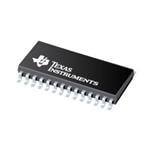
ICGOO电子元器件商城为您提供ADS7824UB由Texas Instruments设计生产,在icgoo商城现货销售,并且可以通过原厂、代理商等渠道进行代购。 ADS7824UB价格参考¥172.74-¥265.52。Texas InstrumentsADS7824UB封装/规格:数据采集 - 模数转换器, 12 Bit Analog to Digital Converter 4 Input 1 SAR 28-SOIC。您可以下载ADS7824UB参考资料、Datasheet数据手册功能说明书,资料中有ADS7824UB 详细功能的应用电路图电压和使用方法及教程。
Texas Instruments 的 ADS7824UB 是一款 12 位、4 通道、采样率为 100kSPS 的模数转换器(ADC),采用 16 引脚 TSSOP 封装。该器件适用于需要中等精度和采样速率的数据采集系统。其典型应用场景包括:

1. 工业自动化与过程控制:用于采集温度、压力、流量等传感器信号,适用于工业监测与控制系统。

2. 电池供电设备:ADS7824UB 具有低功耗特性,适合便携式或低功耗系统,如手持式测量仪器、远程数据采集终端。

3. 电机控制与电源监控:可用于采集电机电流、电压反馈信号,实现精确的控制与保护功能。

4. 医疗设备:适用于便携式医疗监测设备,如血糖仪、心率监测仪等,用于采集生理信号。

5. 测试与测量仪器:如数据记录仪、示波器前端模块,用于多通道信号采集。

6. 消费类电子产品:用于需要多通道模拟信号采集的智能家电、环境监测设备等。

该芯片内置采样保持电路和参考电压,简化了外围设计,适合中精度数据采集需求的应用场合。
| 参数 | 数值 |
| 产品目录 | 集成电路 (IC)半导体 |
| 描述 | IC 12-BIT 4-CH SMPL A/D 28-SOIC模数转换器 - ADC 4-Channel 12-Bit Sampling CMOS |
| 产品分类 | |
| 品牌 | Texas Instruments |
| 产品手册 | |
| 产品图片 |
|
| rohs | 符合RoHS无铅 / 符合限制有害物质指令(RoHS)规范要求 |
| 产品系列 | 数据转换器IC,模数转换器 - ADC,Texas Instruments ADS7824UB- |
| 数据手册 | |
| 产品型号 | ADS7824UB |
| 产品培训模块 | http://www.digikey.cn/PTM/IndividualPTM.page?site=cn&lang=zhs&ptm=13240 |
| 产品目录页面 | |
| 产品种类 | 模数转换器 - ADC |
| 位数 | 12 |
| 供应商器件封装 | 28-SOIC |
| 信噪比 | 73 dB |
| 分辨率 | 12 bit |
| 制造商产品页 | http://www.ti.com/general/docs/suppproductinfo.tsp?distId=10&orderablePartNumber=ADS7824UB |
| 包装 | 管件 |
| 单位重量 | 730.800 mg |
| 商标 | Texas Instruments |
| 安装类型 | 表面贴装 |
| 安装风格 | SMD/SMT |
| 封装 | Tube |
| 封装/外壳 | 28-SOIC(0.295",7.50mm 宽) |
| 封装/箱体 | SOIC-28 |
| 工作温度 | -40°C ~ 85°C |
| 工作电源电压 | 5 V |
| 工厂包装数量 | 20 |
| 接口类型 | Parallel, Serial (SPI) |
| 数据接口 | 串行,并联 |
| 最大功率耗散 | 50 mW |
| 最大工作温度 | + 85 C |
| 最小工作温度 | - 40 C |
| 标准包装 | 20 |
| 特性 | - |
| 电压参考 | Internal, External |
| 电压源 | 单电源 |
| 系列 | ADS7824 |
| 结构 | SAR |
| 转换器数 | 1 |
| 转换器数量 | 1 |
| 转换速率 | 40 kS/s |
| 输入数和类型 | 4 个单端,双极 |
| 输入类型 | Single-Ended |
| 通道数量 | 4 Channel |
| 采样率(每秒) | 40k |


- 商务部:美国ITC正式对集成电路等产品启动337调查
- 曝三星4nm工艺存在良率问题 高通将骁龙8 Gen1或转产台积电
- 太阳诱电将投资9.5亿元在常州建新厂生产MLCC 预计2023年完工
- 英特尔发布欧洲新工厂建设计划 深化IDM 2.0 战略
- 台积电先进制程称霸业界 有大客户加持明年业绩稳了
- 达到5530亿美元!SIA预计今年全球半导体销售额将创下新高
- 英特尔拟将自动驾驶子公司Mobileye上市 估值或超500亿美元
- 三星加码芯片和SET,合并消费电子和移动部门,撤换高东真等 CEO
- 三星电子宣布重大人事变动 还合并消费电子和移动部门
- 海关总署:前11个月进口集成电路产品价值2.52万亿元 增长14.8%


PDF Datasheet 数据手册内容提取
® ADS7824 ADS7824 ADS7824 www.burr-brown.com/databook/ADS7824.html 4 Channel, 12-Bit Sampling CMOS A/D Converter FEATURES DESCRIPTION l 25m s max SAMPLING AND CONVERSION The ADS7824 can acquire and convert 12 bits to l SINGLE +5V SUPPLY OPERATION within – 0.5 LSB in 25m s max while consuming only 50mW max. Laser-trimmed scaling resistors provide l PIN-COMPATIBLE WITH 16-BIT ADS7825 the standard industrial – 10V input range and channel- l PARALLEL AND SERIAL DATA OUTPUT to-channel matching of – 0.1%. The ADS7824 is a l 28-PIN 0.3" PLASTIC DIP AND SOIC low-power 12-bit sampling A/D with a four channel l – 0.5 LSB max INL AND DNL input multiplexer, S/H, clock, reference, and a parallel/serial microprocessor interface. It can be con- l 50mW max POWER DISSIPATION figured in a continuous conversion mode to sequen- l 50m W POWER DOWN MODE tially digitize all four channels. The 28-pin ADS7824 l – 10V INPUT RANGE, FOUR CHANNEL is available in a plastic 0.3" DIP and in a SOIC, both MULTIPLEXER fully specified for operation over the industrial –40(cid:176) C l CONTINUOUS CONVERSION MODE to +85(cid:176) C range. Continuous Conversion Channel CONTC A0 A1 40kW R/C(cid:13) AIN 0 Successive Approximation Register(cid:13) CS(cid:13) Clock and Control Logic (cid:13) 20kW 8kW PWRD 40kW CDAC AIN 1 BUSY(cid:13) 20kW 8kW 40kW Serial(cid:13) DATACLK(cid:13) AIN2 Comparator Data(cid:13) Out(cid:13) SDATA(cid:13) 20kW 8kW or(cid:13) Parallel(cid:13) (cid:13) 40kW AIN Data(cid:13) 8 3 D7-D0(cid:13) Out 20kW 8kW Buffer Internal(cid:13) BYTE CAP +2.5V Ref 6kW REF International Airport Industrial Park • Mailing Address: PO Box 11400, Tucson, AZ 85734 • Street Address: 6730 S. Tucson Blvd., Tucson, AZ 85706 • Tel: (520) 746-1111 • Twx: 910-952-1111 Internet: http://www.burr-brown.com/ • FAXLine: (800) 548-6133 (US/Canada Only) • Cable: BBRCORP • Telex: 066-6491 • FAX: (520) 889-1510 • Immediate Product Info: (800) 548-6132 ® ©1996 Burr-Brown Corporation PDS-11303B APriDnteSd in7 U8.S2.A4. October, 1997 SBAS044
SPECIFICATIONS ELECTRICAL At T = –40(cid:176)C to +85(cid:176)C, f = 40kHz, V = V = V = +5V – 5%, using external reference, CONTC = 0V, unless otherwise specified. A S S1 S2 S ADS7824P, U ADS7824PB, UB PARAMETER CONDITIONS MIN TYP MAX MIN TYP MAX UNITS RESOLUTION 12 [(1) Bits ANALOG INPUT Voltage Range – 10V [ V Impedance Channel On or Off 45.7 [ kW Capacitance 35 [ pF THROUGHPUT SPEED Conversion Time 20 [ m s Acquisition Time 5 [ m s Multiplexer Settling Time Includes Acquisition 5 [ m s Complete Cycle (Acquire and Convert) 25 [ m s Complete Cycle (Acquire and Convert) CONTC = +5V 40 [ m s Throughput Rate 40 [ kHz DC ACCURACY Integral Linearity Error – 0.15 – 1 [ – 0.5 LSB(2) Differential Linearity Error – 0.15 – 1 [ – 0.5 LSB No Missing Codes Guaranteed [ Transition Noise(3) 0.1 [ LSB Full Scale Error(4) Internal Reference – 0.5 – 0.25 % Full Scale Error Drift Internal Reference – 7 – 5 ppm/(cid:176)C Full Scale Error(4) – 0.5 – 0.25 % Full Scale Error Drift – 2 [ ppm/(cid:176)C Bipolar Zero Error – 10 [ mV Bipolar Zero Error Drift – 2 [ ppm/(cid:176)C Channel-to-Channel Mismatch – 0.1 – 0.1 % Power Supply Sensitivity +4.75 < VS < +5.25 – 0.5 [ LSB AC ACCURACY Spurious-Free Dynamic Range(5) fIN = 1kHz 80 90 [ [ dB Total Harmonic Distortion f = 1kHz –90 –80 [ [ dB IN Signal-to-(Noise+Distortion) fIN = 1kHz 70 73 72 [ dB Signal-to-Noise fIN = 1kHz 70 73 72 [ dB Channel Separation(6) f = 1kHz 90 100 [ [ dB IN –3dB Bandwidth 2 [ MHz Useable Bandwidth(7) 90 [ kHz SAMPLING DYNAMICS Aperture Delay 40 [ ns Transient Response(8) FS Step 5 [ m s Overvoltage Recovery(9) 1 [ m s REFERENCE Internal Reference Voltage 2.48 2.5 2.52 [ [ [ V Internal Reference Source Current 1 [ m A (Must use external buffer) External Reference Voltage Range 2.3 2.5 2.7 [ [ [ V for Specified Linearity External Reference Current Drain VREF = +2.5V 100 [ m A DIGITAL INPUTS Logic Levels V –0.3 +0.8 [ [ V IL V +2.4 V +0.3V [ [ V IH S IIL – 10 [ m A I – 10 [ m A IH DIGITAL OUTPUTS Data Format Parallel in two bytes; Serial [ Data Coding Binary Two's Complement [ V I = 1.6mA +0.4 [ V OL SINK V I = 500m A +4 [ V OH SOURCE Leakage Current High-Z State, VOUT = 0V to VS – 5 [ m A Output Capacitance High-Z State 15 [ pF The information provided herein is believed to be reliable; however, BURR-BROWN assumes no responsibility for inaccuracies or omissions. BURR-BROWN assumes no responsibility for the use of this information, and all use of such information shall be entirely at the user’s own risk. Prices and specifications are subject to change without notice. No patent rights or licenses to any of the circuits described herein are implied or granted to any third party. BURR-BROWN does not authorize or warrant any BURR-BROWN product for use in life support devices and/or systems. ® ADS7824 2
SPECIFICATIONS (CONT) ELECTRICAL At T = –40(cid:176)C to +85(cid:176)C, f = 40kHz, V = V = V = +5V – 5%, using external reference, CONTC = 0V, unless otherwise specified. A S S1 S2 S ADS7824P, U ADS7824PB, UB PARAMETER CONDITIONS MIN TYP MAX MIN TYP MAX UNITS DIGITAL TIMING Bus Access Time PAR/SER = +5V 83 [ ns Bus Relinquish Time PAR/SER = +5V 83 [ ns Data Clock PAR/SER = 0V Internal Clock (Output only when EXT/INT LOW 0.5 1.5 [ [ MHz transmitting data) External Clock EXT/INT HIGH 0.1 10 [ [ MHz POWER SUPPLIES V = V = V +4.75 +5 +5.25 [ [ [ V S1 S2 S Power Dissipation f = 40kHz 50 [ mW S PWRD HIGH 50 [ m W TEMPERATURE RANGE Specified Performance –40 +85 [ [ (cid:176)C Storage –65 +150 [ [ (cid:176)C Thermal Resistance (q ) JA Plastic DIP 75 [ (cid:176)C/W SOIC 75 [ (cid:176)C/W NOTES: (1) An asterik ([) specifies same value as grade to the left. (2) LSB means Least Significant Bit. For the 12-bit, – 10V input ADS7824, one LSB is 4.88mV. (3) Typical rms noise at worst case transitions and temperatures. (4) Full scale error is the worst case of –Full Scale or +Full Scale untrimmed deviation from ideal first and last code transitions, divided by the transition voltage (not divided by the full-scale range) and includes the effect of offset error. (5) All specifications in dB are referred to a full-scale – 10V input. (6) A full scale sinewave input on one channel will be attenuated by this amount on the other channels. (7) Useable Bandwidth defined as Full-Scale input frequency at which Signal-to-(Noise+Distortion) degrades to 60dB, or 10 bits of accuracy. (8) The ADS7824 will accurately acquire any input step if given a full acquisition period after the step. (9) Recovers to specified performance after 2 x FS input overvoltage, and normal acquisitions can begin. PACKAGE/ORDERING INFORMATION PACKAGE MINIMUM SIGNAL- DRAWING TEMPERATURE MAXIMUM INTEGRAL TO-(NOISE + DISTORTION) PRODUCT PACKAGE NUMBER(1) RANGE LINEARITY ERROR (LSB) RATIO (dB) ADS7824P Plastic Dip 246 –40(cid:176)C to +85(cid:176)C – 1 70 ADS7824PB Plastic Dip 246 –40(cid:176)C to +85(cid:176)C – 0.5 72 ADS7824U SOIC 217 –40(cid:176)C to +85(cid:176)C – 1 70 ADS7824UB SOIC 217 –40(cid:176)C to +85(cid:176)C – 0.5 72 NOTE: (1) For detailed drawing and dimension table, please see end of data sheet, or Appendix C of Burr-Brown IC Data Book. ABSOLUTE MAXIMUM RATINGS PIN CONFIGURATION Analog Inputs: AIN0, AIN1, AIN2, AIN3 ..............................................– 15V Top View DIP/SOIC REF ...................................(AGND2 –0.3V) to (VS + 0.3V) CAP ........................................Indefinite Short to AGND2, Momentary Short to VS VVS1 taon Vd VS.2.. .t.o.. .A..G...N..D...2...............................................................................................................................................–..0...73VV AGND1(cid:13) 1(cid:13) 28(cid:13) VS1(cid:13) S1 S2 Difference between AGND1, AGND2 and DGND.............................– 0.3V AIN(cid:13) 2(cid:13) 27(cid:13) V (cid:13) 0 S2 Digital Inputs and Outputs..........................................–0.3V to (V + 0.3V) S Maximum Junction Temperature.....................................................150(cid:176)C AIN1(cid:13) 3(cid:13) 26(cid:13) PWRD(cid:13) Internal Power Dissipation.............................................................825mW Lead Temperature (soldering, 10s)................................................+300(cid:176)C AIN2(cid:13) 4(cid:13) 25(cid:13) CONTC(cid:13) Maximum Input Current to Any Pin.................................................100mA AIN(cid:13) 5(cid:13) 24(cid:13) BUSY(cid:13) 3 CAP(cid:13) 6(cid:13) 23(cid:13) CS(cid:13) ELECTROSTATIC REF(cid:13) 7(cid:13) 22(cid:13) R/C(cid:13) DISCHARGE SENSITIVITY ADS7824 (cid:13) AGND2(cid:13) 8(cid:13) 21(cid:13) BYTE(cid:13) (cid:13) This integrated circuit can be damaged by ESD. Burr-Brown TRI-STATE(cid:13) D7(cid:13) 9(cid:13) 20(cid:13) PAR/SER(cid:13) recommends that all integrated circuits be handled with TRI-STATE(cid:13) D6(cid:13) 10(cid:13) 19(cid:13) A0(cid:13) appropriate precautions. Failure to observe proper handling and installation procedures can cause damage. TRI-STATE(cid:13) D5(cid:13) 11(cid:13) 18(cid:13) A1(cid:13) ESD damage can range from subtle performance degrada- EXT/INT(cid:13) D4(cid:13) 12(cid:13) 17(cid:13) D0(cid:13) TAG(cid:13) tion to complete device failure. Precision integrated circuits SYNC D3(cid:13) 13(cid:13) 16(cid:13) D1(cid:13) SDATA(cid:13) may be more susceptible to damage because very small DGND 14 15 D2 DATACLK parametric changes could cause the device not to meet its published specifications. ® 3 ADS7824
PIN ASSIGNMENTS PIN # NAME I/O DESCRIPTION 1 AGND1 Analog Ground. Used internally as ground reference point. 2 AIN Analog Input Channel 0. Full-scale input range is – 10V. 0 3 AIN1 Analog Input Channel 1. Full-scale input range is – 10V. 4 AIN Analog Input Channel 2. Full-scale input range is – 10V. 2 5 AIN Analog Input Channel 3. Full-scale input range is – 10V. 3 6 CAP Internal Reference Output Buffer. 2.2m F Tantalum to ground. 7 REF Reference Input/Output. Outputs +2.5V nominal. If used externally, must be buffered to maintain ADS7825 accuracy. Can also be driven by external system reference. In both cases, bypass to ground with a 2.2m F Tantalum capacitor. 8 AGND2 Analog Ground. 9 D7 O Parallel Data Bit 7 if PAR/SER HIGH; Tri-state if PAR/SER LOW. See Table I. 10 D6 O Parallel Data Bit 6 if PAR/SER HIGH; Tri-state if PAR/SER LOW. See Table I. 11 D5 O Parallel Data Bit 5 if PAR/SER HIGH; Tri-state if PAR/SER LOW. See Table I. 12 D4 I/O Parallel Data Bit 4 if PAR/SER HIGH; if PAR/SER LOW, a LOW level input here will transmit serial data on SDATA from the previous conversion using the internal serial clock; a HIGH input here will transmit serial data using an external serial clock input on DATACLK (D2). See Table I. 13 D3 O Parallel Data Bit 3 if PAR/SER HIGH; SYNC output if PAR/SER LOW. See Table I. 14 DGND Digital Ground. 15 D2 I/O Parallel Data Bit 2 if PAR/SER HIGH; if PAR/SER LOW, this will output the internal serial clock if EXT/INT (D4) is LOW; will be an input for an external serial clock if EXT/INT (D4) is HIGH. See Table I. 16 D1 O Parallel Data Bit 1 if PAR/SER HIGH; SDATA serial data output if PAR/SER LOW. See Table I. 17 D0 I/O Parallel Data Bit 0 if PAR/SER HIGH; TAG data input if PAR/SER LOW. See Table I. 18 A1 I/O Channel Address. Input if CONTC LOW, output if CONTC HIGH. See Table I. 19 A0 I/O Channel Address. Input if CONTC LOW, output if CONTC HIGH. See Table I. 20 PAR/SER I Select Parallel or Serial Output. If HIGH, parallel data will be output on D0 thru D7. If LOW, serial data will be output on SDATA. See Table I and Figure 1. 21 BYTE I Byte Select. Only used with parallel data, when PAR/SER HIGH. Determines which byte is available on D0 thru D7. Changing BYTE with CS LOW and R/C HIGH will cause the data bus to change accordingly. LOW selects the 8 MSBs; HIGH selects the 4 LSBs, see Figures 2 and 3. 22 R/C I Read/Convert Input. With CS LOW, a falling edge on R/C puts the internal sample/hold into the hold state and starts a conversion. With CS LOW, a rising edge on R/C enables the output data bits if PAR/SER HIGH, or starts transmission of serial data if PAR/SER LOW and EXT/INT HIGH. 23 CS I Chip Select. Internally OR'd with R/C. With CONTC LOW and R/C LOW, a falling edge on CS will initiate a conversion. With R/C HIGH, a falling edge on CS will enable the output data bits if PAR/SER HIGH, or starts transmission of serial data if PAR/SER LOW and EXT/INT HIGH. 24 BUSY O Busy Output. Falls when conversion is started; remains LOW until the conversion is completed and the data is latched into the output register. In parallel output mode, output data will be valid when BUSY rises, so that the rising edge can be used to latch the data. 25 CONTC I Continuous Conversion Input. If LOW, conversions will occur normally when initiated using CS and R/C; if HIGH, acquisition and conversions will take place continually, cycling through all four input channels, as long as CS, R/C and PWRD are LOW. See Table I. For serial mode only. 26 PWRD I Power Down Input. If HIGH, conversions are inhibited and power consumption is significantly reduced. Results from the previous conversion are maintained in the output register. In the continuous conversion mode, the multiplexer address channel is reset to channel 0 27 V Supply Input. Nominally +5V. Connect directly to pin 28. Decouple to ground with 0.1m F ceramic and 10m F Tantalum S2 capacitors. 28 VS1 Supply Input. Nominally +5V. Connect directly to pin 27. ® ADS7824 4
TYPICAL PERFORMANCE CURVES At TA = +25(cid:176)C, fS = 40kHz, VS1 = VS2 = +5V, using internal reference, unless otherwise noted. FREQUENCY SPECTRUM(cid:13) ADJACENT CHANNEL CROSSTALK, WORST PAIR(cid:13) (8192 Point FFT; f = 1.02kHz, –0.5dB) (8192 Point FFT; AIN = 1.02kHz, –0.1dB; AIN = AGND) IN 3 2 0(cid:13) 0(cid:13) –10.0(cid:13) –10.0(cid:13) –20.0(cid:13) –20.0(cid:13) –30.0(cid:13) –30.0(cid:13) B) B) d –40.0(cid:13) d –40.0(cid:13) e ( e ( d –50.0(cid:13) d –50.0(cid:13) u u plit –60.0(cid:13) plit –60.0(cid:13) m m A –70.0(cid:13) A –70.0(cid:13) –80.0(cid:13) –80.0(cid:13) –90.0(cid:13) –90.0(cid:13) –100.0(cid:13) –100.0(cid:13) –110.0 –110.0 0 5 10 15 20 0 5 10 15 20 Frequency (kHz) Frequency (kHz) ADJACENT CHANNEL CROSSTALK, WORST PAIR(cid:13) (8192 Point FFT; AIN = 10.1kHz, –0.1dB; AIN = AGND) 3 2 0(cid:13) 0.3(cid:13) dB) ––––12340000....0000(cid:13)(cid:13)(cid:13)(cid:13) 12-Bit LSBs ––0000....21012(cid:13)(cid:13)(cid:13)(cid:13)(cid:13) All Codes INL e ( –0.3 ud –50.0(cid:13) 0 512 1024 1536 2048 2560 3072 3584 4095 plit –60.0(cid:13) Decimal Code m A –70.0(cid:13) 0.3(cid:13) –80.0(cid:13) 0.2(cid:13) All Codes DNL –90.0(cid:13) SBs 0.1(cid:13) ––110100..00(cid:13) 12-Bit L ––00..012(cid:13)(cid:13)(cid:13) 0 5 10 15 20 –0.3 Frequency (kHz) 0 512 1024 1536 2048 2560 3072 3584 4095 Decimal Code ENDPOINT ERRORS 2(cid:13) INL/DNPOL WDEEGRR SAUDPAPTLIOY NR IPPEPRLE L SSBE NOSFI TPI-VPIT RYIP(cid:13) PLE deal 1(cid:13) BPZ Error 1(cid:13) om I 0(cid:13) Fr B) mV –1(cid:13) LS 10–1(cid:13) –2 B/ LS 0.2(cid:13) egradation ( 1100––23(cid:13)(cid:13) INL Percent(cid:13)From Ideal 0(cid:13)(cid:13)(cid:13) +FS Error D y –0.2 nearit 10–4(cid:13) 0.2(cid:13) Li 10–5101 102 103 104 DNL105 106 107 Percent(cid:13)From Ideal 0(cid:13)(cid:13)(cid:13) –FS Error Power Supply Ripple Frequency (Hz) –0.2 –50 –25 0 25 50 75 100 Temperature (°C) ® 5 ADS7824
TYPICAL PERFORMANCE CURVES (CONT) At TA = +25(cid:176)C, fS = 40kHz, VS1 = VS2 = +5V, using internal reference, unless otherwise noted. INTERNAL REFERENCE VOLTAGE(cid:13) vs TEMPERATURE CONVERSION TIME vs TEMPERATURE 2.520(cid:13) 15.7(cid:13) 15.6(cid:13) 2.515(cid:13) 15.5(cid:13) V) 2.510(cid:13) s) nce ( 2.505(cid:13) me (µ 15.4(cid:13) al Refere 22..540905(cid:13)(cid:13) ersion Ti 1155..32(cid:13)(cid:13) n v 15.1(cid:13) Inter 2.490(cid:13) Con 15.0(cid:13) 2.485(cid:13) 14.9(cid:13) 2.480 14.8(cid:13) –50 –25 0 25 50 75 100 –50 –25 0 25 50 75 100 (cid:13) Temperature (°C) Temperature (°C) ® ADS7824 6
BASIC OPERATION PARALLEL OUTPUT SERIAL OUTPUT Figure 1a shows a basic circuit to operate the ADS7824 with Figure 1b shows a basic circuit to operate the ADS7824 with parallel output (Channel 0 selected). Taking R/C (pin 22) serial output (Channel 0 selected). Taking R/C (pin 22) LOW for 40ns (12m s max) will initiate a conversion. BUSY LOW for 40ns (12m s max) will initiate a conversion and (pin 24) will go LOW and stay LOW until the conversion is output valid data from the previous conversion on SDATA completed and the output register is updated. If BYTE (pin (pin 16) synchronized to 12 clock pulses output on 21) is LOW, the 8 most significant bits will be valid when DATACLK (pin 15). BUSY (pin 24) will go LOW and stay pin 24 rises; if BYTE is HIGH, the 4 least significant bits LOW until the conversion is completed and the serial data will be valid when BUSY rises. Data will be output in has been transmitted. Data will be output in Binary Two’s Binary Two’s Complement format. BUSY going HIGH can Complement format, MSB first, and will be valid on both the be used to latch the data. After the first byte has been read, rising and falling edges of the data clock. BUSY going BYTE can be toggled allowing the remaining byte to be HIGH can be used to latch the data. All convert commands read. All convert commands will be ignored while BUSY is will be ignored while BUSY is LOW. LOW. The ADS7824 will begin tracking the input signal at the end The ADS7824 will begin tracking the input signal at the end of the conversion. Allowing 25m s between convert com- of the conversion. Allowing 25m s between convert com- mands assures accurate acquisition of a new signal. mands assures accurate acquisition of a new signal. Parallel Output 1(cid:13) 28(cid:13) 0.1µF 10µF ±10V 2(cid:13) 27(cid:13) + + +5V 3(cid:13) 26(cid:13) 4(cid:13) 25(cid:13) BUSY 5(cid:13) 24(cid:13) + 6(cid:13) 23(cid:13) Convert Pulse 2.2µF R/C + 7(cid:13) 22(cid:13) 2.2µF (cid:13) ADS7824 BYTE 8(cid:13) 21(cid:13) 40ns min 9(cid:13)(cid:13) 20(cid:13) +5V(1) 10(cid:13) 19(cid:13) 11(cid:13) 18(cid:13) 12(cid:13) 17(cid:13) 13(cid:13) 16(cid:13) 14 15 Serial Output Pin 21(cid:13) D11(cid:13) D10 D9 D8 D7 D6 D5 D4 LOW (cid:13) 1(cid:13) 28(cid:13) Pin 21(cid:13) D3 D2 D1 D0 LOW LOWLOWLOW 0.1µF 10µF HIGH ±10V 2(cid:13) 27(cid:13) + + +5V NOTE: (1) PAR/SER = 5V 3(cid:13) 26(cid:13) 4(cid:13) 25(cid:13) 5(cid:13) 24(cid:13) BUSY + 6(cid:13) 23(cid:13) Convert Pulse 2.2µF + 7(cid:13) 22(cid:13) R/C 2.2µF (cid:13) ADS7824 8(cid:13) 21(cid:13) 40ns min NC(2) 9(cid:13)(cid:13) 20(cid:13) (3) NC(2) 10(cid:13) 19(cid:13) NC(2) 11(cid:13) 18(cid:13) EXT/INT 12(cid:13) 17(cid:13) SYNC 13(cid:13) 16(cid:13) SDATA 14 15 DATACLK(1) NOTES: (1) DATACLK (pin 15) is an output when EXT/INT (pin 12) is LOW(cid:13) and an input when EXT/INT is HIGH. (2) NC = no connection. (3) PAR/SER = 0V. FIGURE 1. Basic Connection Diagram, (a) Parallel Output, (b) Serial Output. ® 7 ADS7824
STARTING A CONVERSION The combination of CS (pin 23) and R/C (pin 22) LOW for initiating a conversion. If, however, it is critical that CS or a minimum of 40ns places the sample/hold of the ADS7824 R/C initiates conversion ‘n’, be sure the less critical input is in the hold state and starts conversion ‘n’. BUSY (pin 24) LOW at least 10ns prior to the initiating input. If EXT/INT will go LOW and stay LOW until conversion ‘n’ is com- (pin 12) is LOW when initiating conversion ‘n’, serial data pleted and the internal output register has been updated. All from conversion ‘n – 1’ will be output on SDATA (pin 16) new convert commands during BUSY LOW will be ignored. following the start of conversion ‘n’. See Internal Data CS and/or R/C must go HIGH before BUSY goes HIGH or Clock in the Reading Data section. a new conversion will be initiated without sufficient time to To reduce the number of control pins, CS can be tied LOW acquire a new signal. using R/C to control the read and convert modes. This will The ADS7824 will begin tracking the input signal at the end have no effect when using the internal data clock in the serial of the conversion. Allowing 25m s between convert com- output mode. However, the parallel output and the serial mands assures accurate acquisition of a new signal. Refer to output (only when using an external data clock) will be Tables Ia and Ib for a summary of CS, R/C, and BUSY states affected whenever R/C goes HIGH. Refer to the Reading and Figures 2 through 6 and Table II for timing information. Data section and Figures 2, 3, 5, and 6. CS and R/C are internally OR’d and level triggered. There is not a requirement which input goes LOW first when INPUTS OUTPUTS CS R/C BYTE CONTC PWRD BUSY D7 D6 D5 D4 D3 D2 D1 D0 COMMENTS 1 X X X X X Hi-Z Hi-Z Hi-Z Hi-Z Hi-Z Hi-Z Hi-Z Hi-Z X 0 X X X X Hi-Z Hi-Z Hi-Z Hi-Z Hi-Z Hi-Z Hi-Z Hi-Z 0 1 0 X X X D11 D10 D9 D8 D7 D6 D5 D4 Results from last (MSB) completed conversion. 0 1 1 X X X D3 D2 D1 D0 LOW LOW LOW LOW Results from last (LSB) completed conversion. 0 1 X X X › ›fl fl› fl› ›fl ›fl fl› ›fl ›fl Data will change at the end of a conversion. TABLE Ia. Read Control for Parallel Data (PAR/SER = 5V.) D7, D6, D5 D4 D3 D2 D1 D0 CS R/C CONTC PWRD BUSY LOW EXT/INT SYNC DATACLK SDATA TAG Input Input Input Input Output Output Input Output I/O Output Input COMMENTS 1 X X X 1 Hi-Z LOW LOW Output Hi-Z X X 0 X X 1 Hi-Z LOW LOW Output Hi-Z X 0 fl 0 X 1 Hi-Z LOW LOW Output Output X Starts transmission of data from previous conversion on SDATA synchronized to 12 pulses output on DATACLK. fl 0 0 X 1 Hi-Z LOW LOW Output Output X Starts transmission of data from previous conversion on SDATA synchronized to 12 pulses output on DATACLK. 0 1 0 X X Hi-Z HIGH LOW Input Output Input The level output on SDATA will be the level input on TAG 12 DATACLK input cycles earlier. 0 1 0 X › Hi-Z HIGH LOW Input Output Input At the end of the conversion, when BUSY rises, data from the conversion will be shifted into the output registers. If DATACLK is HIGH, valid data will be lost. 0 › 0 X 1 Hi-Z HIGH LOW Input Output X Initiates transmission of a HIGH pulse on SYNC followed by data from last completed conversion on SDATA synchronized to the input on DATACLK. fl 1 0 X 1 Hi-Z HIGH LOW Input Output X Initiates transmission of a HIGH pulse on SYNC followed by data from last completed conversion on SDATA synchronized to the input on DATACLK. 0 0 1 0 fl Hi-Z LOW LOW Output Output X Starts transmission of data from previous conversion on SDATA synchronized to 12 pulses output on DATACLK fl 1 X X X Hi-Z HIGH Output Input Output X SDATA becomes active. Inputs on DATACLK shift out data. 0 › X X X Hi-Z HIGH Output Input Output X SDATA becomes active. Inputs on DATACLK shift out data. fl 0 1 X X Hi-Z LOW LOW Output Output X Restarts continuous conversion mode (n – 1 data transmitted when BUSY is LOW). 0 fl 1 X X Hi-Z LOW LOW Output Output X Restarts continuous conversion mode (n – 1 data transmitted when BUSY is LOW). TABLE Ib. Read Control for Serial Data (PAR/SER = 0V.) ® ADS7824 8
t t 1 1 R/C t t 3 3 t 4 BUSY t 5 t6 t6 t t 7 8 MODE Acquire Convert Acquire Convert t t 12 t 12 11 t 10 Parallel(cid:13) Previous(cid:13) Previous High(cid:13) Previous Low(cid:13) High Byte(cid:13) Low Byte(cid:13) High Byte(cid:13) Hi-Z Not Valid Hi-Z Data Bus High Byte Valid Byte Valid Byte Valid Valid Valid Valid t t 2 9 t9 t12 t12 t12 t12 BYTE FIGURE 2. Conversion Timing with Parallel Output (CS LOW). t t t t t t 21 21 21 21 21 21 R/C t 1 CS t 3 t BUSY 4 t t t t 21 21 21 21 BYTE DATA(cid:13) Hi-Z State High Byte Hi-Z State Low Byte Hi-Z State BUS t t t t 12 9 12 9 FIGURE 3. Using CS to Control Conversion and Read Timing with Parallel Outputs. CS or R/C(1) t7 + t8 t14 DATACLK t13 1 2 3 11 12 1 2 t16 t15 SDATA MSB Valid Bit 10 Valid Bit 9 Valid Bit 1 Valid LSB Valid MSB Valid Bit 10 Valid Hi-Z Hi-Z t25 (Results from previous conversion.) BUSY t26 NOTE: (1) If controlling with CS, tie R/C LOW. If controlling with R/C, tie CS LOW. FIGURE 4. Serial Data Timing Using Internal Data Clock (TAG LOW). ® 9 ADS7824
t28 t22 Tag 0 Tag 13 14 0 (LSB) ag 12 Bit T 3 1 1 1 1 Bit ag T n. o si r e v n 4 Bit 10 Tag 2 r Co e ft A 3 B) ad Bit 11 (MS Tag 1 GH). Re I 2 t24 ag 0 NT H T I t17 T/ X E ( 1 t20 t23 ck o t17 t19 t21 t27 nal Cl t180 xter E h wit g n mi Ti d a e R t1 t21 t3 nd a n o si r e v n o C 5. TERNAL(cid:13)TACLK CS R/C BUSY SYNC SDATA TAG GURE XA ED FI ® ADS7824 10
t22 t28 ults). s e R ag 0T Tag 13 ersion v n o C Bit 0 (LSB) Tag 12 Previous ( n o si r e v n o C g n t11 MSB) g 1 Duri Bit 11 ( Ta Read ). H G t24 HI T t17 IN T/ ag 0 EX T ( t23 t27 ck o t20 Cl al n r e xt E h t19 t1 wit t17 ng t18 t3 mi Ti t21 ead R d n a n o si r e L(cid:13) S C Y C A G v ERNAACLK C R/ BUS SYN SDAT TA Con EXTDAT E 6. R U G I F ® 11 ADS7824
READING DATA after the start of conversion ‘n’. Do not attempt to read data beyond 12m s after the start of conversion ‘n’ until BUSY PARALLEL OUTPUT (pin 24) goes HIGH; this may result in reading invalid data. To use the parallel output, tie PAR/SER (pin 20) HIGH. The Refer to Table II and Figures 2 and 3 for timing constraints. parallel output will be active when R/C (pin 22) is HIGH and CS (pin 23) is LOW. Any other combination of CS and R/C SERIAL OUTPUT will tri-state the parallel output. Valid conversion data can be When PAR/SER (pin 20) is LOW, data can be clocked out read in two 8-bit bytes on D7-D0 (pins 9-13 and 15-17). When serially with the internal data clock or an external data clock. BYTE (pin 21) is LOW, the 8 most significant bits will be When EXT/INT (pin 12) is LOW, DATACLK (pin 15) is an valid with the MSB on D7. When BYTE is HIGH, the 4 least output and is always active regardless of the state of CS (pin significant bits will be valid with the LSB on D4. BYTE can 23) and R/C (pin 22). The SDATA output is active when be toggled to read both bytes within one conversion cycle. BUSY (pin 24) is LOW. Otherwise, it is in a tri-state Upon initial power up, the parallel output will contain condition. When EXT/INT is HIGH, DATACLK is an input. indeterminate data. The SDATA output is active when CS is LOW and R/C is HIGH. Otherwise, it is in a tri-state condition. Regardless of PARALLEL OUTPUT (After a Conversion) the state of EXT/INT, SYNC (pin 13) is an output and always active, while TAG (pin 17) is always an input. After conversion ‘n’ is completed and the output registers have been updated, BUSY (pin 24) will go HIGH. Valid data from conversion ‘n’ will be available on D7-D0 (pins 9-13 INTERNAL DATA CLOCK (During A Conversion) and 15-17). BUSY going HIGH can be used to latch the To use the internal data clock, tie EXT/INT (pin 12) LOW. data. Refer to Table II and Figures 2 and 3 for timing The combination of R/C (pin 22) and CS (pin 23) LOW will constraints. initiate conversion ‘n’ and activate the internal data clock (typically 900kHz clock rate). The ADS7824 will output 12 PARALLEL OUTPUT (During a Conversion) bits of valid data, MSB first, from conversion ‘n – 1’ on SDATA (pin 16), synchronized to 12 clock pulses output on After conversion ‘n’ has been initiated, valid data from conversion ‘n – 1’ can be read and will be valid up to 12m s DATACLK (pin 15). The data will be valid on both the SYMBOL DESCRIPTION MIN TYP MAX UNITS t1 Convert Pulse Width 0.04 12 m s t Start of Conversion to New Data Valid 15 21 m s 2 t Start of Conversion to BUSY LOW 85 ns 3 t4 BUSY LOW 15 21 m s t End of Conversion to BUSY HIGH 90 ns 5 t6 Aperture Delay 40 ns t Conversion Time 15 21 m s 7 t8 Acquisition Time 3 5 m s t + t Throughput Time 25 m s 7 8 t9 Bus Relinquish Time 10 83 ns t Data Valid to BUSY HIGH 20 60 ns 10 t11 Start of Conversion to Previous Data Not Valid 12 15 m s t Bus Access Time and BYTE Delay 83 ns 12 t13 Start of Conversion to DATACLK Delay 1.4 m s t DATACLK Period 1.1 m s 14 t Data Valid to DATACLK HIGH 20 75 ns 15 t16 DATACLK LOW to Data Not Valid 400 600 ns t External DATACLK Period 100 ns 17 t18 External DATACLK HIGH 50 ns t External DATACLK LOW 40 ns 19 t20 CS LOW and R/C HIGH to External DATACLK HIGH (Enable Clock) 25 ns t R/C to CS Setup Time 10 ns 21 t22 CS HIGH or R/C LOW to External DATACLK HIGH (Disable Clock) 25 ns t DATACLK HIGH to SYNC HIGH 15 35 ns 23 t24 DATACLK HIGH to Valid Data 25 55 ns t Start of Conversion to SDATA Active 83 ns 25 t26 End of Conversion to SDATA Tri-State 83 ns t CS LOW and R/C HIGH to SDATA Active 83 ns 27 t CS HIGH or R/C LOW to SDATA Tri-State 83 ns 28 t29 BUSY HIGH to Address Valid 20 ns t Address Valid to BUSY LOW 500 ns 30 TABLE II. Conversion, Data, and Address Timing. T = –40(cid:176) C to +85(cid:176) C. A ® ADS7824 12
rising and falling edges of the internal data clock. The rising 14th falling edge and the 15th rising edge of DATACLK; the edge of BUSY (pin 24) can be used to latch the data. After second input bit will be valid on the 15th falling edge and the the 12th clock pulse, DATACLK will remain LOW until the 16th rising edge, etc. With a continuous data clock, TAG next conversion is initiated, while SDATA will go to what- data will be output on DATA until the internal output ever logic level was input on TAG (pin 17) during the first registers are updated with the results from the next conver- clock pulse. The SDATA output will tri-state when BUSY sion. Refer to Table II and Figure 5 for timing information. returns HIGH. Refer to Table II and Figure 4 for timing information. EXTERNAL DATA CLOCK (During a Conversion) After conversion ‘n’ has been initiated, valid data from EXTERNAL DATA CLOCK conversion ‘n – 1’ can be read and will be valid up to 12m s To use an external clock, tie EXT/INT (pin 12) HIGH. The after the start of conversion ‘n’. Do not attempt to clock out external clock is not a conversion clock; it can only be used data from 12m s after the start of conversion ‘n’ until BUSY as a data clock. To enable the output mode of the ADS7824, (pin 24) rises; this will result in data loss. CS (pin 23) must be LOW and R/C (pin 22) must be HIGH. NOTE: For the best possible performance when using an DATACLK must be HIGH for 20% to 70% of the total data external data clock, data should not be clocked out during a clock period; the clock rate can be between DC and 10MHz. conversion. The switching noise of the asynchronous data Serial data from conversion ‘n’ can be output on SDATA clock can cause digital feedthrough degrading the converter’s (pin 16) after conversion ‘n’ is completed or during conver- performance. Refer to Table II and Figure 6 for timing sion ‘n + 1’. information. An obvious way to simplify control of the converter is to tie CS LOW while using R/C to initiate conversions. While this TAG FEATURE is perfectly acceptable, there is a possible problem when TAG (pin 17) inputs serial data synchronized to the external using an external data clock. At an indeterminate point from or internal data clock. 12m s after the start of conversion ‘n’ until BUSY rises, the internal logic will shift the results of conversion ‘n’ into the When using an external data clock, the serial bit stream input output register. If CS is LOW, R/C is HIGH and the external on TAG will follow the LSB output on SDATA (pin 16) clock is HIGH at this point, data will be lost. So, with CS until the internal output register is updated with new conver- LOW, either R/C and/or DATACLK must be LOW during sion results. See Table II and Figures 5 and 6. this period to avoid losing valid data. The logic level input on TAG for the first rising edge of the internal data clock will be valid on SDATA after all 12 bits EXTERNAL DATA CLOCK (After a Conversion) of valid data have been output. After conversion ‘n’ is completed and the output registers have been updated, BUSY (pin 24) will go HIGH. With CS MULTIPLEXER TIMING LOW (pin 23) and R/C HIGH (pin 22), valid data from The four channel input multiplexer may be addressed manu- conversion ‘n’ will be output on SDATA (pin 16) synchro- ally or placed in a continuous conversion mode where all nized to the external data clock input on DATACLK (pin four channels are sequentially addressed. 15). Between 15 and 35ns following the rising edge of the first external data clock, the SYNC output pin will go HIGH CONTINUOUS CONVERSION MODE (CONTC= 5V) for one full data clock period (100ns minimum). The MSB To place the ADS7824 in the continuous conversion mode, will be valid between 25 and 55ns after the rising edge of the CONTC (pin 25) must be tied HIGH. In this mode, acquisi- second data clock. The LSB will be valid on the 13th falling tion and conversions will take place continually, cycling edge and the 14th rising edge of the data clock. TAG (pin through all four channels as long as CS, R/C and PWRD are 17) will input a bit of data for every external clock pulse. LOW (See Table III). Whichever address was last loaded The first bit input on TAG will be valid on SDATA on the CONTC CS R/C BUSY PWRD A0 and A1 OPERATION 0 X X X X Inputs Initiating conversion n latches in the levels input on A0 and A1 to select the channel for conversion 'n + 1'. 0 X X 0 0 Inputs Conversion in process. New convert commands ignored. 0 0 fl 1 0 Inputs Initiates conversion on channel selected at start of previous conversion. 0 fl 0 1 0 Inputs Initiates conversion on channel selected at start of previous conversion. 0 X X X 1 Inputs All analog functions powered down. Conversions in process or initiated will yield meaningless data. 1 X X X X Outputs The end of conversion n (when BUSY rises) increments the internal channel latches and outputs the channel address for conversion 'n + 1' on A0 and A1. 1 X X 0 0 Outputs Conversion in process. 1 0 fl 1 0 Outputs Restarts continuous conversion process on next input channel. 1 fl 0 1 0 Outputs Restarts continuous conversion process on next input channel. 1 X X X 1 Outputs All analog functions powered down. Conversions in process or initiated will yield meaningless data. Resets selected input channel for next conversion to AIN. 0 TABLE III. Conversion Control. ® 13 ADS7824
into the A0 and A1 registers (pins 19 and 18, respectively) conversions will proceed through each higher channel, prior to CONTC being raised HIGH, becomes the first cycling back to zero after Channel 3. address in the sequential continuous conversion mode (e.g., If PWRD is held HIGH for a significant period of time, the if Channel 1 was the last address selected then Channel 2 will REF (pin 7) bypass capacitor may discharge (if the internal follow, then Channel 3, and so on). The A0 and A1 address reference is being utilized) and the CAP (pin 6) bypass inputs become outputs when the device is in this mode. capacitor will discharge (for both internal and external When BUSY rises at the end of a conversion, A0 and A1 will references). The continuous conversion mode should not be output the address of the channel that will be converted when enabled until the bypass capacitor(s) have recharged and BUSY goes LOW at the beginning of the next conversion. stabilized (1ms for 2.2m F capacitors recommended). In Data will be valid for the previous channel after BUSY rises. addition, the continuous conversion mode should not be The address lines are updated when BUSY rises. See Table enabled even with a short pulse on PWRD until the mini- IVa and Figure 7 for channel selection timing in continuous mum acquisition time has been met. conversion mode. PWRD (pin 26) can be used to reset the multiplexer address MANUAL CHANNEL SELECTION (CONTC= 0V) to zero. With the ADS7824 configured for no conversion, The channels of the ADS7824 can be selected manually by PWRD can be taken HIGH for a minimum of 200ns. When using the A0 and A1 address pins (pins 19 and 18, respec- PWRD returns LOW, the multiplexer address will be reset to tively). See Table IVb for the multiplexer truth table and zero. When the continuous conversion mode is enabled, the Figure 8 for channel selection timing. first conversion will be done on Channel 0. Subsequent ADS7824 TIMING AND CONTROL DATA AVAILABLE CHANNEL TO BE A1 A0 FROM CHANNEL OR BEING CONVERTED DESCRIPTION OF OPERATION 0 0 AIN3 AIN0 Channel being acquired or converted is output on these 0 1 AIN0 AIN1 address lines. Data is valid for the previous channel. These 1 0 AIN AIN 1 2 lines are updated when BUSY rises. 1 1 AIN2 AIN3 TABLE IVa. A0 and A1 Outputs (CONTC HIGH). CHANNEL SELECTED A1 A0 WHEN BUSY GOES HIGH DESCRIPTION OF OPERATION 0 0 AIN0 Channel to be converted during conversion 'n + 1' is latched 0 1 AIN1 when conversion 'n' is initiated (BUSY goes LOW). The selected 1 0 AIN2 input starts being acquired as soon as conversion 'n' is done 1 1 AIN3 (BUSY goes HIGH). TABLE IVb. A0 and A1 Inputs (CONTC LOW). Conversion Currently in Progress: BUSY n – 2 n – 1 n n + 1 n + 2 n + 3 n + 4 Channel Address for Conversion: A0, A1(cid:13) n – 2 n – 1 n n + 1 n + 2 n + 3 n + 4 n + 5 (Output) t 29 Results from Conversion: D7-D0 n – 3 n – 2 n – 1 n n + 1 n + 2 n + 3 n + 4 FIGURE 7. Channel Addressing in Continuous Conversion Mode (CONTC HIGH, CS and R/C LOW). R/C Conversion Currently in Progress: BUSY n – 2 n – 1 n n + 1 n + 2 n + 3 n + 4 Channel Address for Conversion: A0, A1(cid:13) n – 1 n n + 1 n + 2 n + 3 n + 4 n + 5 (Input) t 30 Results from Conversion: D7-D0 n – 3 n – 2 n – 1 n n + 1 n + 2 n + 3 n + 4 FIGURE 8. Channel Addressing in Normal Conversion Mode (CONTC and CS LOW). ® ADS7824 14
CALIBRATION CDAC. Capacitor values larger than 2.2(F will have little affect on improving performance. The ADS7824 has no internal provision for correcting the The output of the buffer is capable of driving up to 1mA of individual bipolar zero error or full-scale error for each current to a DC load. Using an external buffer will allow the individual channel. Instead, the bipolar zero error of each internal reference to be used for larger DC loads and AC channel is guaranteed to be below a level which is quite loads. Do not attempt to directly drive an AC load with the small for a converter with a – 10V input range (slightly more output voltage on CAP. This will cause performance degra- than – 2 LSBs). In addition, the channel errors should match dation of the converter. each other to within 1 LSB. For the full-scale error, the circuit of Figure 9 can be used. PWRD This will allow the reference to be adjusted such that the PWRD (pin 26) HIGH will power down all of the analog full-scale error for any single channel can be set to zero. circuitry including the reference. Data from the previous Again, the close matching of the channels will ensure that conversion will be maintained in the internal registers and the full-scale errors on the other channels will be small. can still be read. With PWRD HIGH, a convert command yields meaningless data. When PWRD is returned LOW, adequate time must be provided in order for the capacitors AIN2 on REF (pin 7) and CAP (pin 6) to recharge. For 2.2m F capacitors, a minimum recharge/settling time of 1ms is AIN recommended before the conversion results should be con- 3 sidered valid. CAP +5V R(cid:13) (cid:13)+ 1M1W 2.2µF LAYOUT P1(cid:13) REF 50kW + 2.2µF POWER AGND2 The ADS7824 uses 90% of its power for the analog cir- cuitry, and the converter should be considered an analog component. For optimum performance, tie both power pins FIGURE 9. Full Scale Trim. to the same +5V power supply and tie the analog and digital grounds together. The +5V power for the converter should be separate from REFERENCE the +5V used for the system’s digital logic. Connecting V S1 The ADS7824 can operate with its internal 2.5V reference or and VS2 (pins 28 and 27) directly to a digital supply can an external reference. By applying an external reference to reduce converter performance due to switching noise from pin 7, the internal reference can be bypassed. the digital logic. For best performance, the +5V supply can be produced from whatever analog supply is used for the rest of the analog signal conditioning. If +12V or +15V supplies REF are present, a simple +5V regulator can be used. Although it REF (pin 7) is an input for an external reference or the output is not suggested, if the digital supply must be used to power for the internal 2.5V reference. A 2.2m F capacitor should be the converter, be sure to properly filter the supply. Either connected as close to the REF pin as possible. This capacitor using a filtered digital supply or a regulated analog supply, and the output resistance of REF create a low pass filter to both V and V should be tied to the same +5V source. S1 S2 bandlimit noise on the reference. Using a smaller value capacitor will introduce more noise to the reference degrad- GROUNDING ing the SNR and SINAD. The REF pin should not be used to drive external AC or DC loads. Three ground pins are present on the ADS7824. DGND is the digital supply ground. AGND2 is the analog supply The range for the external reference is 2.3V to 2.7V and ground. AGND1 is the ground which all analog signals determines the actual LSB size. Increasing the reference internal to the A/D are referenced. AGND1 is more suscep- voltage will increase the full scale range and the LSB size of tible to current induced voltage drops and must have the path the converter which can improve the SNR. of least resistance back to the power supply. All the ground pins of the A/D should be tied to an analog CAP ground plane, separated from the system’s digital logic CAP (pin 6) is the output of the internal reference buffer. A ground, to achieve optimum performance. Both analog and 2.2m F capacitor should be placed as close to the CAP pin as digital ground planes should be tied to the ‘system’ ground possible to provide optimum switching currents for the as near to the power supplies as possible. This helps to CDAC throughout the conversion cycle. This capacitor also prevent dynamic digital ground currents from modulating provides compensation for the output of the buffer. Using a the analog ground through a common impedance to power capacitor any smaller than 1m F can cause the output buffer ground. to oscillate and may not have sufficient charge for the ® 15 ADS7824
CROSSTALK minimal requirement for the drive capability on the signal With a full-scale 1kHz input signal, worst case crosstalk on conditioning preceding the A/D. Any op amp sufficient for the ADS7824 is better than –95dB. This should be adequate the signal in an application will be sufficient to drive the for even the most demanding applications. However, if ADS7824. crosstalk is a concern, the following items should be kept in The resistive front end of the ADS7824 also provides a mind: guaranteed – 15V overvoltage protection. In most cases, this The worst case crosstalk is generally from Channel 3 to 2. In eliminates the need for external over voltage protection addition, crosstalk from Channel 3 to any other channel is circuitry. worse than from those channels to Channel 3. The reason for this is that channel three is nearer to the reference on the INTERMEDIATE LATCHES ADS7824. This allows two coupling modes: channel-to- The ADS7824 does have tri-state outputs for the parallel channel and Channel 3 to the reference. In general, when port, but intermediate latches should be used if the bus will crosstalk is a concern, avoid placing signals with higher be active during conversions. If the bus is not active during frequency components on Channel 3. conversions, the tri-state outputs can be used to isolate the If a particular channel should be as immune as possible from A/D from other peripherals on the same bus. crosstalk, Channel 0 would be the best channel for the signal Intermediate latches are beneficial on any monolithic A/D and Channel 1 should have the signal with the lowest converter. The ADS7824 has an internal LSB size of 610m V. frequency content. If two signals are to have as little crosstalk Transients from fast switching signals on the parallel port, as possible, they should be placed on Channel 0 and Channel even when the A/D is tri-stated, can be coupled through the 2 with lower frequency, less-sensitive inputs on the other substrate to the analog circuitry causing degradation of channels. converter performance. The effect of this phenomenon will be more obvious when using the pin-compatible ADS7825 SIGNAL CONDITIONING or any of the other 16-bit converters in the ADS Family. This The FET switches used for the sample hold on many CMOS is due to the smaller LSB size of 38m V. A/D converters release a significant amount of charge injec- For an ADS7824 with proper layout, grounding, and bypass- tion which can cause the driving op amp to oscillate. The ing; the effect should only be a few tenths of an LSB at the amount of charge injection due to the sampling FET switch most. In those cases where this is not true, it is possible for on the ADS7824 is approximately 5-10% of the amount on the conversion results to exhibit random errors of many similar ADCs with the charge redistribution DAC (CDAC) LSBs. Poor grounding, poor bypassing, and high-speed architecture. There is also a resistive front end which attenu- digital signals will increase the magnitude of the errors. ates any charge which is released. The end result is a ® ADS7824 16
PACKAGE OPTION ADDENDUM www.ti.com 6-Feb-2020 PACKAGING INFORMATION Orderable Device Status Package Type Package Pins Package Eco Plan Lead/Ball Finish MSL Peak Temp Op Temp (°C) Device Marking Samples (1) Drawing Qty (2) (6) (3) (4/5) ADS7824U ACTIVE SOIC DW 28 20 Green (RoHS NIPDAU-DCC Level-3-260C-168 HR -40 to 85 ADS7824U & no Sb/Br) ADS7824U/1K ACTIVE SOIC DW 28 1000 Green (RoHS NIPDAU-DCC Level-3-260C-168 HR -40 to 85 ADS7824U & no Sb/Br) ADS7824UB ACTIVE SOIC DW 28 20 Green (RoHS NIPDAU-DCC Level-3-260C-168 HR -40 to 85 ADS7824U & no Sb/Br) B ADS7824UBE4 ACTIVE SOIC DW 28 20 Green (RoHS NIPDAU-DCC Level-3-260C-168 HR -40 to 85 ADS7824U & no Sb/Br) B (1) The marketing status values are defined as follows: ACTIVE: Product device recommended for new designs. LIFEBUY: TI has announced that the device will be discontinued, and a lifetime-buy period is in effect. NRND: Not recommended for new designs. Device is in production to support existing customers, but TI does not recommend using this part in a new design. PREVIEW: Device has been announced but is not in production. Samples may or may not be available. OBSOLETE: TI has discontinued the production of the device. (2) RoHS: TI defines "RoHS" to mean semiconductor products that are compliant with the current EU RoHS requirements for all 10 RoHS substances, including the requirement that RoHS substance do not exceed 0.1% by weight in homogeneous materials. Where designed to be soldered at high temperatures, "RoHS" products are suitable for use in specified lead-free processes. TI may reference these types of products as "Pb-Free". RoHS Exempt: TI defines "RoHS Exempt" to mean products that contain lead but are compliant with EU RoHS pursuant to a specific EU RoHS exemption. Green: TI defines "Green" to mean the content of Chlorine (Cl) and Bromine (Br) based flame retardants meet JS709B low halogen requirements of <=1000ppm threshold. Antimony trioxide based flame retardants must also meet the <=1000ppm threshold requirement. (3) MSL, Peak Temp. - The Moisture Sensitivity Level rating according to the JEDEC industry standard classifications, and peak solder temperature. (4) There may be additional marking, which relates to the logo, the lot trace code information, or the environmental category on the device. (5) Multiple Device Markings will be inside parentheses. Only one Device Marking contained in parentheses and separated by a "~" will appear on a device. If a line is indented then it is a continuation of the previous line and the two combined represent the entire Device Marking for that device. (6) Lead/Ball Finish - Orderable Devices may have multiple material finish options. Finish options are separated by a vertical ruled line. Lead/Ball Finish values may wrap to two lines if the finish value exceeds the maximum column width. Important Information and Disclaimer:The information provided on this page represents TI's knowledge and belief as of the date that it is provided. TI bases its knowledge and belief on information provided by third parties, and makes no representation or warranty as to the accuracy of such information. Efforts are underway to better integrate information from third parties. TI has taken and Addendum-Page 1
PACKAGE OPTION ADDENDUM www.ti.com 6-Feb-2020 continues to take reasonable steps to provide representative and accurate information but may not have conducted destructive testing or chemical analysis on incoming materials and chemicals. TI and TI suppliers consider certain information to be proprietary, and thus CAS numbers and other limited information may not be available for release. In no event shall TI's liability arising out of such information exceed the total purchase price of the TI part(s) at issue in this document sold by TI to Customer on an annual basis. Addendum-Page 2
PACKAGE MATERIALS INFORMATION www.ti.com 29-Sep-2017 TAPE AND REEL INFORMATION *Alldimensionsarenominal Device Package Package Pins SPQ Reel Reel A0 B0 K0 P1 W Pin1 Type Drawing Diameter Width (mm) (mm) (mm) (mm) (mm) Quadrant (mm) W1(mm) ADS7824U/1K SOIC DW 28 1000 330.0 32.4 11.35 18.67 3.1 16.0 32.0 Q1 PackMaterials-Page1
PACKAGE MATERIALS INFORMATION www.ti.com 29-Sep-2017 *Alldimensionsarenominal Device PackageType PackageDrawing Pins SPQ Length(mm) Width(mm) Height(mm) ADS7824U/1K SOIC DW 28 1000 367.0 367.0 55.0 PackMaterials-Page2
IMPORTANTNOTICEANDDISCLAIMER TI PROVIDES TECHNICAL AND RELIABILITY DATA (INCLUDING DATASHEETS), DESIGN RESOURCES (INCLUDING REFERENCE DESIGNS), APPLICATION OR OTHER DESIGN ADVICE, WEB TOOLS, SAFETY INFORMATION, AND OTHER RESOURCES “AS IS” AND WITH ALL FAULTS, AND DISCLAIMS ALL WARRANTIES, EXPRESS AND IMPLIED, INCLUDING WITHOUT LIMITATION ANY IMPLIED WARRANTIES OF MERCHANTABILITY, FITNESS FOR A PARTICULAR PURPOSE OR NON-INFRINGEMENT OF THIRD PARTY INTELLECTUAL PROPERTY RIGHTS. These resources are intended for skilled developers designing with TI products. You are solely responsible for (1) selecting the appropriate TI products for your application, (2) designing, validating and testing your application, and (3) ensuring your application meets applicable standards, and any other safety, security, or other requirements. These resources are subject to change without notice. TI grants you permission to use these resources only for development of an application that uses the TI products described in the resource. Other reproduction and display of these resources is prohibited. No license is granted to any other TI intellectual property right or to any third party intellectual property right. TI disclaims responsibility for, and you will fully indemnify TI and its representatives against, any claims, damages, costs, losses, and liabilities arising out of your use of these resources. TI’s products are provided subject to TI’s Terms of Sale (www.ti.com/legal/termsofsale.html) or other applicable terms available either on ti.com or provided in conjunction with such TI products. TI’s provision of these resources does not expand or otherwise alter TI’s applicable warranties or warranty disclaimers for TI products. Mailing Address: Texas Instruments, Post Office Box 655303, Dallas, Texas 75265 Copyright © 2020, Texas Instruments Incorporated