ICGOO在线商城 > 集成电路(IC) > 数据采集 - 模数转换器 > AD7482BSTZ
 Datasheet下载
- 型号: AD7482BSTZ
- 制造商: Analog
- 库位|库存: xxxx|xxxx
- 要求:
| 数量阶梯 | 香港交货 | 国内含税 |
| +xxxx | $xxxx | ¥xxxx |
查看当月历史价格
查看今年历史价格
AD7482BSTZ产品简介:
ICGOO电子元器件商城为您提供AD7482BSTZ由Analog设计生产,在icgoo商城现货销售,并且可以通过原厂、代理商等渠道进行代购。 AD7482BSTZ价格参考¥101.11-¥183.41。AnalogAD7482BSTZ封装/规格:数据采集 - 模数转换器, 12 Bit Analog to Digital Converter 1 Input 1 SAR 48-LQFP (7x7)。您可以下载AD7482BSTZ参考资料、Datasheet数据手册功能说明书,资料中有AD7482BSTZ 详细功能的应用电路图电压和使用方法及教程。
AD7482BSTZ 是由 Analog Devices Inc. 生产的一款 12 位、双通道模数转换器(ADC),属于数据采集系列。其应用场景主要包括以下几个方面:

 1. 工业自动化与控制
   - AD7482BSTZ 可用于工业自动化系统中的信号采集,例如温度、压力、流量等传感器的模拟信号转换为数字信号。
   - 在多通道数据采集系统中,该器件可以同时处理两个独立的输入信号,适合需要快速切换和高精度测量的应用场景。

 2. 医疗设备
   - 在医疗领域,AD7482BSTZ 可应用于心电图(ECG)、脑电图(EEG)和其他生物医学信号的采集。
   - 其低功耗和高分辨率特性非常适合便携式或电池供电的医疗设备。

 3. 通信系统
   - 该 ADC 可用于通信系统的信号接收部分,将射频(RF)或中频(IF)信号经过下变频后的模拟信号转换为数字信号进行处理。
   - 在基站或无线通信设备中,它能够提供稳定的数据采集性能。

 4. 汽车电子
   - 在汽车电子控制系统中,AD7482BSTZ 可用于发动机控制单元(ECU)、底盘控制和安全系统中的信号采集。
   - 它支持快速采样率(最高可达 1 MSPS),适合需要实时监测和控制的汽车应用。

 5. 测试与测量仪器
   - 该器件适用于示波器、万用表和其他测试设备中的信号采集模块。
   - 其双通道设计和高线性度使其成为多路信号同步测量的理想选择。

 6. 航空航天与国防
   - 在航空航天领域,AD7482BSTZ 可用于飞行器上的传感器数据采集,如惯性导航系统、遥测系统等。
   - 其高可靠性和抗干扰能力满足严苛环境下的使用需求。

 特性总结
- 双通道输入:支持同时采集两个独立信号。
- 12 位分辨率:提供高精度的模数转换。
- 高速采样率:最高可达 1 MSPS,满足实时性要求。
- 低功耗设计:适合便携式和低功耗应用。

综上所述,AD7482BSTZ 广泛应用于需要高精度、高速度和低功耗的数据采集场景,特别是在工业、医疗、通信和汽车等领域表现出色。
| 参数 | 数值 |
| 产品目录 | 集成电路 (IC)半导体 |
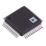
| 描述 | IC ADC 12BIT SAR 3MSPS 48-LQFP模数转换器 - ADC 12-Bit 3 MSPS SAR |
| 产品分类 | |
| 品牌 | Analog Devices |
| 产品手册 | |
| 产品图片 |
|
| rohs | 符合RoHS无铅 / 符合限制有害物质指令(RoHS)规范要求 |
| 产品系列 | 数据转换器IC,模数转换器 - ADC,Analog Devices AD7482BSTZ- |
| 数据手册 | |
| 产品型号 | AD7482BSTZ |
| 产品目录页面 | |
| 产品种类 | 模数转换器 - ADC |
| 位数 | 12 |
| 供应商器件封装 | 48-LQFP(7x7) |
| 分辨率 | 12 bit |
| 包装 | 托盘 |
| 商标 | Analog Devices |
| 安装类型 | 表面贴装 |
| 安装风格 | SMD/SMT |
| 封装 | Tray |
| 封装/外壳 | 48-LQFP |
| 封装/箱体 | LQFP-48 |
| 工作温度 | -40°C ~ 85°C |
| 工作电源电压 | 5 V |
| 工厂包装数量 | 250 |
| 接口类型 | Parallel |
| 数据接口 | 并联 |
| 最大功率耗散 | 90 mW |
| 最大工作温度 | + 85 C |
| 最小工作温度 | - 40 C |
| 标准包装 | 1 |
| 电压参考 | Internal, External |
| 电压源 | 模拟和数字 |
| 系列 | AD7482 |
| 结构 | SAR |
| 转换器数 | 1 |
| 转换器数量 | 1 |
| 转换速率 | 3 MS/s |
| 输入数和类型 | 1 个单端,单极 |
| 输入类型 | Single-Ended |
| 通道数量 | 1 Channel |
| 采样率(每秒) | 3M |


- 商务部:美国ITC正式对集成电路等产品启动337调查
- 曝三星4nm工艺存在良率问题 高通将骁龙8 Gen1或转产台积电
- 太阳诱电将投资9.5亿元在常州建新厂生产MLCC 预计2023年完工
- 英特尔发布欧洲新工厂建设计划 深化IDM 2.0 战略
- 台积电先进制程称霸业界 有大客户加持明年业绩稳了
- 达到5530亿美元!SIA预计今年全球半导体销售额将创下新高
- 英特尔拟将自动驾驶子公司Mobileye上市 估值或超500亿美元
- 三星加码芯片和SET,合并消费电子和移动部门,撤换高东真等 CEO
- 三星电子宣布重大人事变动 还合并消费电子和移动部门
- 海关总署:前11个月进口集成电路产品价值2.52万亿元 增长14.8%


PDF Datasheet 数据手册内容提取
3 MSPS, 12-Bit SAR ADC AD7482 FEATURES FUNCTIONAL BLOCK DIAGRAM Fast throughput rate: 3 MSPS AVDD AGND CBIAS DVDD VDRIVE DGND Wide input bandwidth: 40 MHz No pipeline delays with SAR ADC 2.5V Excellent dc accuracy performance REFERENCE BUF REFOUT 2 parallel interface modes REFSEL REFIN Low power: 90 mW (full power) and 2.5 mW (nap mode) Standby mode: 2 µA maximum 12-BIT Single 5 V supply operation ALGORITHMIC VIN T/H SAR Internal 2.5 V reference Full-scale overrange mode (using 13th bit) AD7482 System offset removal via user access offset register D12 Nominal 0 V to 2.5 V input with shifted range capability MODE1 D11 MODE2 D10 14-bit pin compatible upgrade AD7484 available CLIP CONTROL NAP LOGIC AND I/O D9 STBY REGISTERS D8 D7 RESET D6 CONVST D5 CSRDWRITEBUSYD0D1D2D3D4 02638-001 Figure 1. GENERAL DESCRIPTION The AD7482 is a 12-bit, high speed, low power, successive alive for a quick power-up while consuming 2.5 mW, and a approximation ADC. The part features a parallel interface with standby mode that reduces power consumption to a mere 10 μW. throughput rates up to 3 MSPS. The part contains a low noise, The AD7482 features an on-board 2.5 V reference but can also wide bandwidth track-and-hold that can handle input frequencies accommodate an externally provided 2.5 V reference source. in excess of 40 MHz. The nominal analog input range is 0 V to 2.5 V, but an offset The conversion process is a proprietary algorithmic successive shift capability allows this nominal range to be offset by ±200 mV. approximation technique that results in no pipeline delays. The This allows the user considerable flexibility in setting the bottom input signal is sampled, and a conversion is initiated on the falling end reference point of the signal range, a useful feature when edge of the CONVST signal. The conversion process is controlled using single-supply op amps. via an internally trimmed oscillator. Interfacing is via standard The AD7482 also provides an 8% overrange capability via a parallel signal lines, making the part directly compatible with 13th bit. Therefore, if the analog input range strays outside the microcontrollers and DSPs. nominal by up to 8%, the user can still accurately resolve the The AD7482 provides excellent ac and dc performance specifica- signal by using the 13th bit. tions. Factory trimming ensures high dc accuracy, resulting in The AD7482 is powered by a 4.75 V to 5.25 V supply. The part very low INL, offset, and gain errors. also provides a V pin that allows the user to set the voltage DRIVE The part uses advanced design techniques to achieve very low levels for the digital interface lines. The range for this VDRIVE pin power dissipation at high throughput rates. Power consumption is 2.7 V to 5.25 V. The part is housed in a 48-lead LQFP package in the normal mode of operation is 90 mW. There are two power and is specified over a −40°C to +85°C temperature range. saving modes: a nap mode, which keeps the reference circuitry Rev. B Information furnished by Analog Devices is believed to be accurate and reliable. However, no responsibility is assumed by Analog Devices for its use, nor for any infringements of patents or other One Technology Way, P.O. Box 9106, Norwood, MA 02062-9106, U.S.A. rights of third parties that may result from its use. Specifications subject to change without notice. No license is granted by implication or otherwise under any patent or patent rights of Analog Devices. Tel: 781.329.4700 www.analog.com Trademarks and registered trademarks are the property of their respective owners. Fax: 781.461.3113 ©2002–2009 Analog Devices, Inc. All rights reserved.
AD7482 TABLE OF CONTENTS Features .............................................................................................. 1 Circuit Description......................................................................... 12 Functional Block Diagram .............................................................. 1 Converter Operation .................................................................. 12 General Description ......................................................................... 1 Analog Input ............................................................................... 12 Revision History ............................................................................... 2 ADC Transfer Function ............................................................. 13 Specifications ..................................................................................... 3 Power Saving ............................................................................... 13 Timing Characteristics ................................................................ 5 Offset/Overrange ........................................................................ 14 Absolute Maximum Ratings ............................................................ 6 Parallel Interface ......................................................................... 15 ESD Caution .................................................................................. 6 Board Layout and Grounding ................................................... 17 Pin Configuration and Function Descriptions ............................. 7 Outline Dimensions ....................................................................... 19 Typical Performance Characteristics ............................................. 9 Ordering Guide .......................................................................... 19 Terminology .................................................................................... 11 REVISION HISTORY 12/09—Rev. A to Rev. B Changes to Table 1, Power Requirements Section ....................... 4 Changes to Ordering Guide .......................................................... 19 9/08—Rev. 0 to Rev. A Changes to Table 4 ............................................................................ 7 Changes to Offset/Overrange Section ......................................... 14 Changes to Table 5, Table 6, Table 7 ............................................. 15 Changes to Ordering Guide .......................................................... 19 8/02—Revision 0: Initial Version Rev. B | Page 2 of 20
AD7482 SPECIFICATIONS AV /DV = 5 V ± 5%, AGND = DGND = 0 V, V = external, f = 3 MSPS; all specifications T to T and valid for V = 2.7 V DD DD REF SAMPLE MIN MAX DRIVE to 5.25 V, unless otherwise noted. The operating temperature range is −40°C to +85°C. Table 1. Parameter Min Typ Max Unit Test Conditions/Comments DYNAMIC PERFORMANCE1, 2 Signal-to-Noise + Distortion (SINAD)3 71 dB f = 1 MHz IN 72 dB f = 1 MHz IN 71 dB f = 1 MHz, internal reference IN Total Harmonic Distortion (THD)3 −86 dB −90 dB −88 dB Internal reference Peak Harmonic or Spurious Noise (SFDR)3 −87 dB Intermodulation Distortion (IMD)3 Second Order Terms −96 dB f = 95.053 kHz, IN1 f = 105.329 kHz IN2 Third Order Terms −94 dB Aperture Delay 10 ns Full Power Bandwidth 40 MHz @ 3 dB 3.5 MHz @ 0.1 dB DC ACCURACY Resolution 12 Bits Integral Nonlinearity3 ±0.5 LSB B Grade ±0.25 ±1 LSB A Grade Differential Nonlinearity3 ±0.25 ±0.5 LSB Guaranteed no missed codes to 12 bits Offset Error3 ±1.5 LSB 0.036 %FSR Gain Error3 ±1.5 LSB 0.036 %FSR ANALOG INPUT Input Voltage −200 mV +2.7 V DC Leakage Current ±1 μA V from 0 V to 2.7 V IN ±2 μA V = −200 mV IN Input Capacitance4 35 pF REFERENCE INPUT/OUTPUT Input Voltage, V +2.5 V ±1% for specified performance REFIN Input DC Leakage Current, V ±1 μA REFIN Input Capacitance, V 4 25 pF REFIN Input Current, V 220 μA External reference REFIN Output Voltage, V +2.5 V REFOUT Error @ 25°C, V ±50 mV REFOUT Error T to T , V ±100 mV MIN MAX REFOUT Output Impedance, V 1 Ω REFOUT Rev. B | Page 3 of 20
AD7482 Parameter Min Typ Max Unit Test Conditions/Comments LOGIC INPUTS Input High Voltage, V V − 1 V INH DRIVE Input Low Voltage, V 0.4 V INL Input Current, I ±1 μA IN Input Capacitance, C 4 10 pF IN LOGIC OUTPUTS Output High Voltage, V 0.7 × V V OH DRIVE Output Low Voltage, V 0.4 V OL Floating State Leakage Current ±10 μA Floating State Output Capacitance4 10 pF Output Coding Straight (Natural) Binary CONVERSION RATE Conversion Time 300 ns Track-and-Hold Acquisition Time (t ) 70 ns Sine wave input ACQ 70 ns Full-scale step input Throughput Rate 2.5 MSPS Parallel Mode 1 3 MSPS Parallel Mode 2 POWER REQUIREMENTS AV 5 V ±5% DD DV 5 V ±5% DD V 2.7 5.25 V DRIVE I DD Normal Mode (Static) 13 mA CS and RD = Logic 1 Normal Mode (Operational) 20 mA Nap Mode 0.5 mA Standby Mode 0.5 2 μA Power Dissipation Normal Mode (Operational) 100 mW Nap Mode 2.5 mW Standby Mode5 10 μW 1 SINAD figures quoted include external analog input circuit noise contribution of approximately 1 dB. 2 See the Typical Performance Characteristics section for analog input circuits used. 3 See the Terminology section. 4 Sample tested @ 25°C to ensure compliance. 5 Digital input levels at DGND or VDRIVE. Rev. B | Page 4 of 20
AD7482 TIMING CHARACTERISTICS AV /DV = 5 V ± 5%, AGND = DGND = 0 V, V = external; all specifications T to T and valid for V = 2.7 V to 5.25 V, DD DD REF MIN MAX DRIVE unless otherwise noted. Table 2. Parameter1 Symbol Min Typ Max Unit DATA READ Conversion Time t 300 ns CONV Quiet Time Before Conversion Start t 100 ns QUIET CONVST Pulse width t 5 100 ns 1 CONVST Falling Edge to BUSY Falling Edge t 20 ns 2 CS Falling Edge to RD Falling Edge t 0 ns 3 Data Access Time t 25 ns 4 CONVST Falling Edge to New Data Valid t 30 ns 5 BUSY Rising Edge to New Data Valid t 5 ns 6 Bus Relinquish Time t 10 ns 7 RD Rising Edge to CS Rising Edge t 0 ns 8 CS Pulse width t 30 ns 14 RD Pulse width t 30 ns 15 DATA WRITE WRITE Pulse Width t 5 ns 9 Data Setup Time t 2 ns 10 Data Hold Time t 6 ns 11 CS Falling Edge to WRITE Falling Edge t 5 ns 12 WRITE Falling Edge to CS Rising Edge t 0 ns 13 1 All timing specifications given are with a 25 pF load capacitance. With a load capacitance greater than this value, a digital buffer or latch must be used. Rev. B | Page 5 of 20
AD7482 ABSOLUTE MAXIMUM RATINGS Stresses above those listed under Absolute Maximum Ratings T = 25°C, unless otherwise noted. A may cause permanent damage to the device. This is a stress Table 3. rating only; functional operation of the device at these or any Parameter Rating other conditions above those indicated in the operational AV to AGND −0.3 V to +7 V section of this specification is not implied. Exposure to absolute DD DV to DGND −0.3 V to +7 V maximum rating conditions for extended periods may affect DD V to DGND −0.3 V to +7 V device reliability. DRIVE Analog Input Voltage to AGND −0.3 V to AV + 0.3 V DD Digital Input Voltage to DGND −0.3 V to V + 0.3 V DRIVE ESD CAUTION REFIN to AGND −0.3 V to AV + 0.3 V DD Input Current to Any Pin Except ±10 mA Supply Pins Operating Temperature Range −40°C to +85°C Commercial Storage Temperature Range −65°C to +150°C Junction Temperature 150°C Thermal Impedance, θ 50°C/W JA Thermal Impedance, θ 10°C/W JC Lead Temperature, Soldering Vapor Phase (60 sec) 215°C Infrared (15 sec) 220°C ESD 1 kV Rev. B | Page 6 of 20
AD7482 PIN CONFIGURATION AND FUNCTION DESCRIPTIONS T AGND AGNDAVDDCLIP MODE1 MODE2 RESET CONVSD12 D11 D10 D9 48 47 46 45 44 43 42 41 40 39 38 37 AVDD 1 PIN 1 36 D8 CBIAS 2 IDENTIFIER 35 D7 AGND 3 34 D6 AGND 4 33 D5 AVDD 5 AD7482 32 VDRIVE AGND 6 TOP VIEW 31 DGND VIN 7 (Not to Scale) 30 DGND REFOUT 8 29 DVDD REFIN 9 28 D4 REFSEL 10 27 D3 AGND 11 26 D2 AGND 12 25 D1 13 14 15 16 17 18 19 20 21 22 23 24 AVDDAGND AGND STBY NAP CS RDWRITE BUSYR1 R2 D0 02638-002 Figure 2. Pin Configuration Table 4. Pin Function Descriptions Pin No. Mnemonic Description 1, 5, 13, 46 AV Positive Power Supply for Analog Circuitry. DD 2 C Decoupling Pin for Internal Bias Voltage. A 1 nF capacitor should be placed between this pin and AGND. BIAS 3, 4, 6, 11, 12, AGND Power Supply Ground for Analog Circuitry. 14, 15, 47, 48 7 VIN Analog Input. Single ended analog input channel. 8 REFOUT Reference Output. REFOUT connects to the output of the internal 2.5 V reference buffer. A 470 nF capacitor must be placed between this pin and AGND. 9 REFIN Reference Input. A 470 nF capacitor must be placed between this pin and AGND. When using an external voltage reference source, the reference voltage should be applied to this pin. 10 REFSEL Reference Decoupling Pin. When using the internal reference, a 1 nF capacitor must be connected from this pin to AGND. When using an external reference source, this pin should be connected directly to AGND. 16 STBY Standby Logic Input. When this pin is logic high, the device is placed in standby mode. See the Power Saving section for further details. 17 NAP Nap Logic Input. When this pin is logic high, the device is placed in a very low power mode. See the Power Saving section for further details. 18 CS Chip Select Logic Input. This pin is used in conjunction with RD to access the conversion result. The data bus is brought out of three-state and the current contents of the output register driven onto the data lines following the falling edge of both CS and RD. CS is also used in conjunction with WRITE to perform a write to the offset register. CS can be hardwired permanently low. 19 RD Read Logic Input. Used in conjunction with CS to access the conversion result. 20 WRITE Write Logic Input. Used in conjunction with CS to write data to the offset register. When the desired offset word has been placed on the data bus, the WRITE line should be pulsed high. It is the falling edge of this pulse that latches the word into the offset register. 21 BUSY Busy Logic Output. This pin indicates the status of the conversion process. The BUSY signal goes low after the falling edge of CONVST and stays low for the duration of the conversion. In Parallel Mode 1, the BUSY signal returns high when the conversion result has been latched into the output register. In Parallel Mode 2, the BUSY signal returns high as soon as the conversion has been completed, but the conversion result does not get latched into the output register until the falling edge of the next CONVST pulse. 22, 23 R1, R2 No Connect. These pins should be pulled to ground via 100 kΩ resistors. 24 to 28, D0 to D11 Data I/O Bits. D11 is MSB. These are three-state pins that are controlled by CS, RD, and WRITE. The operating 33 to 39 voltage level for these pins is determined by the V input. DRIVE 29 DV Positive Power Supply for Digital Circuitry. DD Rev. B | Page 7 of 20
AD7482 Pin No. Mnemonic Description 30, 31 DGND Ground Reference for Digital Circuitry. 32 V Logic Power Supply Input. The voltage supplied at this pin determines at what voltage the interface logic of DRIVE the device operates. 40 D12 Data Output Bit for Overranging. If the overrange feature is not used, this pin should be pulled to DGND via a 100 kΩ resistor. 41 CONVST Convert Start Logic Input. A conversion is initiated on the falling edge of the CONVST signal. The input track- and-hold amplifier goes from track mode to hold mode, and the conversion process commences. 42 RESET Reset Logic Input. An active low reset pulse must be applied to this pin after power-up to ensure correct operation. A falling edge on this pin resets the internal state machine and terminates a conversion that may be in progress. The contents of the offset register are also cleared on this edge. Holding this pin low keeps the part in a reset state. 43 MODE2 Operating Mode Logic Input. See Table 8 for details. 44 MODE1 Operating Mode Logic Input. See Table 8 for details. 45 CLIP Logic Input. A logic high on this pin enables output clipping. In this mode, any input voltage that is greater than positive full scale or less than negative full scale is clipped to all 1s or all 0s, respectively. Further details are given in the Offset/Overrange section. Rev. B | Page 8 of 20
AD7482 TYPICAL PERFORMANCE CHARACTERISTICS 0 0.5 fIN = 10.7kHz SNR = 72.97dB 0.4 SNR + D = 72.94dB –20 THD = –91.5dB 0.3 0.2 –40 0.1 B) SB) (d –60 L (L 0 N I–0.1 –80 –0.2 –0.3 –100 –0.4 –1200 200 400 FR6E0Q0UENC80Y0 (kHz)1000 1200 1400 02638-003 –0.50 1024 ADC2 0(4C8ode) 3072 4096 02638-006 Figure 3. 64k FFT Plot With 10 kHz Input Tone Figure 6. Typical INL 0 80 fIN = 1.013MHz SNR = 72.58dB SNR + D = 72.57dB –20 THD = –94.0dB –40 75 B) (dB) –60 AD (d N SI –80 70 –100 –1200 200 400 FR60E0QUEN8C0Y0 (kHz1)000 1200 1400 02638-004 6510 IN10P0UT FREQUENCY (1k0H0z0) 10000 02638-007 Figure 4. 64k FFT Plot With 1 MHz Input Tone Figure 7. SINAD vs. Input Tone (AD8021 Input Circuit) 0.5 –40 0.4 200Ω 100Ω 0.3 –50 0.2 –60 B) 0.1 B) DNL (LS–0.10 THD (d –70 10Ω 51Ω –0.2 –80 0Ω –0.3 –90 –0.4 –0.50 1024 ADC2 0(4C8ode) 3072 4096 02638-005 –100100 INPUT FRE1Q0U00ENCY (kHz) 10000 02638-008 Figure 5. Typical DNL Figure 8. THD vs. Input Tone for Different Input Resistances Rev. B | Page 9 of 20
AD7482 0 0.0004 100mV p-p SINE WAVE ON SUPPLY PINS –10 0 –20 –0.0004 –30 B) V) RR (d–40 OUT (–0.0008 S F P E –50 R –0.0012 –60 –0.0016 –70 –8010 FREQUE1N00CY (kHz) 1000 02638-009 –0.0020–55 –25 5TEMPER3A5TURE (°C6)5 95 125 02638-010 Figure 9. PSRR Without Decoupling Figure 10. Reference Out Error Rev. B | Page 10 of 20
AD7482 TERMINOLOGY Integral Nonlinearity Total Harmonic Distortion (THD) The integral nonlinearity is the maximum deviation from a The THD is the ratio of the rms sum of the harmonics to the straight line passing through the endpoints of the ADC transfer fundamental. It is defined as function. The endpoints of the transfer function are zero scale, a V 2+V 2+V 2+V 2+V 2 point 1/2 LSB below the first code transition, and full scale, a THD(dB)=20log 2 3 4 5 6 point 1/2 LSB above the last code transition. V 1 Differential Nonlinearity where V is the rms amplitude of the fundamental and V, V, 1 2 3 The differential nonlinearity is the difference between the V, V, and V are the rms amplitudes of the second through the 4 5 6 measured and ideal 1 LSB change between any two adjacent sixth harmonics. codes in the ADC. Peak Harmonic or Spurious Noise Offset Error The peak harmonic or spurious noise is the ratio of the rms The offset error is the deviation of the first code transition value of the next largest component in the ADC output spectrum (00...000) to (00...001) from the ideal, that is, AGND + 0.5 LSB. (up to f/2 and excluding dc) to the rms value of the fundamental. S The value of this specification is usually determined by the largest Gain Error harmonic in the spectrum, but for ADCs where the harmonics The gain error is the deviation of the last code transition are buried in the noise floor, it is a noise peak. (111...110) to (111...111) from the ideal, that is, V − 1.5 LSB REF after the offset error is adjusted out. Intermodulation Distortion With inputs consisting of sine waves at two frequencies, fa and Track-and-Hold Acquisition Time fb, any active device with nonlinearities creates distortion products Track-and-hold acquisition time is the time required for the at sum and difference frequencies of mfa ± nfb, where m and n = 0, output of the track-and-hold amplifier to reach its final value, 1, 2, 3, and so on. Intermodulation distortion terms are those for within ±1/2 LSB, after the end of conversion (the point at which which neither m nor n is equal to zero. For example, the second the track-and-hold returns to track mode). order terms include (fa + fb) and (fa − fb), wehreas the third order Signal-to-Noise + Distortion (SINAD) Ratio terms include (2fa + fb), (2fa − fb), (fa + 2fb), and (fa − 2fb ). The SINAD ratio is the measured ratio of signal-to-noise + The AD7482 is tested using the CCIF standard, where two input distortion at the output of the ADC. The signal is the rms frequencies near the top end of the input bandwidth are used. In amplitude of the fundamental. Noise is the sum of all nonfunda- this case, the second order terms are usually distanced in frequency mental signals up to half the sampling frequency (f/2), excluding S from the original sine waves, whereas the third order terms are dc. The ratio is dependent on the number of quantization levels usually at a frequency close to the input frequencies. As a result, in the digitization process; the more levels, the smaller the the second order and third order terms are specified separately. quantization noise. The theoretical SINAD ratio for an ideal N-bit The calculation of the intermodulation distortion is as per the converter with a sine wave input is given by: THD specification, where it is the ratio of the rms sum of the Signal-to-Noise + Distortion = (6.02N +1.76)dB individual distortion products to the rms amplitude of the sum Therefore, this is 74 dB for a 12-bit converter. of the fundamentals expressed in dBs. Rev. B | Page 11 of 20
AD7482 CIRCUIT DESCRIPTION CONVERTER OPERATION At the end of conversion, the track-and-hold returns to track mode and the acquisition time begins. The track-and-hold The AD7482 is a 12-bit algorithmic successive approximation acquisition time is 40 ns. Figure 13 shows the ADC during its ADC based around a capacitive DAC. It provides the user with acquisition phase. SW2 is closed and SW1 is in Position A. The track-and-hold, reference, an ADC, and versatile interface logic comparator is held in a balanced condition and the sampling functions on a single chip. The normal analog input signal range capacitor acquires the signal on V . that the AD7482 can convert is 0 V to 2.5 V. By using the offset IN and overrange features on the ADC, the AD7482 can convert CAPACITIVE analog input signals from −200 mV to +2.7 V while operating DAC from a single 5 V supply. The part requires a 2.5 V reference, which can be provided from the internal reference or an external A reference source. Figure 11 shows a simplified schematic of the VIN + ADC. The control logic, SAR, and capacitive DAC are used to SW1 B CONTROL LOGIC add and subtract fixed amounts of charge from the sampling SW2 – COMPARATOR capacitor to bring the comparator bacCkO MtoP AaR AbTaOlaRnced condition. AGND 02638-015 Figure 13. ADC Acquisition Phase CAPACITIVE DAC ANALOG INPUT +VS VIN 8 VREF SWITCHES SIGNAACL 1kΩ 100Ω 3 + 7 BIAS 1kΩ AD829 6 VIN SAR VOLTAGE 2 – 4 5 1 –VS COINNTPRUOTSL COLNOTGRICOL 12O-BUITTP PUATR DAALTLAEL 02638-013 Figure 14. Analog Input Ci1r5c0uΩit Used f2o2r0 1p0F kHz Input Tone02638-011 Figure 11. Simplified Block Diagram of the AD7482 Conversion is initiated on the AD7482 by pulsing the CONVST input. On the falling edge of CONVST, the track-and-hold goes +VS from track mode to hold mode and the conversion sequence is 8 started. Conversion time for the part is 300 ns. Figure 12 shows SIGNAACL 50Ω 2 + 7 the ADC during conversion. When conversion starts, SW2 AD8021 6 VIN opens and SW1 moves to Position B, causing the comparator to VOLTBAIGASE 220Ω 3 – 4 become unbalanced. The ADC then runs through its successive- 5 1 approximation routine and brings the comparator back into a 10pF balanced condition. When the comparator is rebalanced, the –VS 220Ω conversion result is available in the SAR register. CAPACITIVE 10pF 02638-012 DAC Figure 15. Analog Input Circuit Used for 1 MHz Input Tone Figure 14 shows the analog input circuit used to obtain the data A for the fast fourier transfer (FFT) plot shown in Figure 3. The VIN + circuit uses an AD829 op amp as the input buffer. A bipolar analog SW1 CONTROL LOGIC B signal is applied and biased up with a stable, low noise dc voltage SW2 – COMPARATOR connected to the labeled terminal, as shown in Figure 11. A 220 pF AGND 02638-014 caonmd tpheen asantaiolong cgarpoaucnitdo rp ilsa nceo.n Tnheec tAedD b8e2t9w iese snu Pppinli e5d a nwdit hth +e 1A2D V8 29 Figure 12. ADC Conversion Phase and −12 V supplies. The supply pins are decoupled as close to the device as possible with both a 0.1 µF and a 10 µF capacitor connected to each pin. In each case, 0.1 µF capacitor should be the closer of the two caps to the device. More information on the AD829 is available at www.analog.com. Rev. B | Page 12 of 20
AD7482 For higher input bandwidth applications, the AD8021 op amp For the remaining 700 ns of the cycle, the AD7482 dissipates (also available as a dual AD8022 op amp) is the recommended 42 mW of power. choice to drive the AD7482. Figure 15 shows the analog input (700 ns/1 μs) × (5 V × 12 mA) = 42 mW circuit used to obtain the data for the FFT plot shown in Figure 4. A Therefore, the power dissipated during each cycle is bipolar analog signal is applied to the terminal and biased up with a stable, low noise dc voltage connected, as shown in Figure 12. A 27 mW + 42 mW = 69 mW 10 pF compensation capacitor is connected between Pin 5 of the Figure 17 shows the AD7482 conversion sequence operating in AD8021 and the negative supply. The AD8021 is supplied with normal mode. +12 V and −12 V supplies. The supply pins are decoupled as close 1µs to the device as possible, with both a 0.1 μF an ad 10 μF capacitor connected to each pin. In each case, the 0.1 μF capacitor should CONVST be the closer of the two caps to the device. The AD8021 logic reference pin is tied to analog ground and the DISABLE Pin is BUSY tiniefdo rtom tahteio pno sointi vteh esu ApDply8,0 a2s1 s hiso awvna iilna bFlieg uatr ew 1w2.w D.aentaaliolegd.c om. 300ns 700ns 02638-017 Figure 17. Normal Mode Power Dissipation ADC TRANSFER FUNCTION In nap mode, almost all the internal circuitry is powered down. The output coding of the AD7482 is straight binary. The designed In this mode, the power dissipation is reduced to 2.5 mW. When code transitions occur midway between the successive integer using an external reference, there must be a minimum of 300 ns LSB values, that is, 1/2 LSB, 3/2 LSB, and so on. The LSB size is from exiting nap mode to initiating a conversion. This is necessary V /4096. The nominal transfer characteristic for the AD7482 is REF to allow the internal circuitry to settle after power-up and for shown in Figure 16. This transfer characteristic may be shifted the track-and-hold to properly acquire the analog input signal. as detailed in the Offset/Overrange section. The internal reference cannot be used in conjunction with the nap mode. 111...111 111...110 If the AD7482 is put into nap mode after each conversion, the average power dissipation is reduced, but the throughput rate is E OD111...000 limited by the power-up time. Using the AD7482 with a through- C C011...111 1LSB = VREF/4096 put rate of 500 kSPS while placing the part in nap mode after D A each conversion results in average power dissipation as follows: 000...010 000...001 The power-up phase contributes 000...000 0V 0.5LSB ANALOG INPUT+VREF – 1.5LSB 02638-016 (300 ns/2 μs) × (5 V × 12 mA) = 9 mW Figure 16. AD7482 Transfer Characteristic The conversion phase contributes POWER SAVING (300 ns/2 μs) × (5 V × 18 mA) = 13.5 mA The AD7482 uses advanced design techniques to achieve very While in nap mode for the rest of the cycle, the AD7482 low power dissipation at high throughput rates. In addition, the dissipates only 1.75 mW of power. AD7482 features two power saving modes, nap and standby. These (1400 ns/2 μs) × (5 V × 0.5 mA) = 1.75 mW modes are selected by bringing either the NAP pin or STBY pin Therefore, the power dissipated during each cycle is to a logic high, respectively. 9 mW + 13.5 mW + 1.75 mW = 24.25 mW When operating the AD7482 in normal fully powered mode, the current consumption is 18 mA during conversion and the quiescent current is 12 mA. Operating at a throughput rate of 1 MSPS, the conversion time of 300 ns contributes 27 mW to the overall power dissipation. (300 ns/1 μs) × (5 V × 18 mA) = 27 mW Rev. B | Page 13 of 20
AD7482 Figure 18 shows the AD7482 conversion sequence when the reference source is used and kept powered up while the AD7482 is part is put into nap mode after each conversion. in standby mode, the power-up time required is reduced to 80 µs. 600ns 1400ns OFFSET/OVERRANGE NAP The AD7482 provides a ±8% overrange capability as well as a 300ns programmable offset register. The overrange capability is achieved by the use of a 13th bit (D12) and the CLIP input. If the CLIP input CONVST is at logic high and the contents of the offset register are 0, then the AD7482 operates as a normal 12-bit ADC. If the input voltage is BUSY 2µs 02638-018 gavrlolel t1aatsge. erS ,t ithmhaein ld atrahlteya , f oiuful ltt-hpsuec ati lnferp ovumotl tvtahogelet ,Aa tghDee C ids ialsto aaw lole u0rts pt. huInat n ftrh otihmse c atzhseeer, o AD-Ds1c2Ca l eis Figure 18. Nap Mode Power Dissipation acts as an overrange indicator. It is set to 1 if the analog input Figure 19 and Figure 20 show a typical graphical representation voltage is outside the nominal 0 V to 2.5 V range. of power vs. throughput for the AD7482 when in normal mode The default contents of the offset register are 0. If the offset register and nap mode, respectively. contains any value other than 0, the contents of the register are 90 added to the SAR result at the end of conversion. This has the effect of shifting the transfer function of the ADC as shown in Figure 21 85 and Figure 22. Note that with the CLIP input set to logic high, the maximum and minimum codes that the AD7482 can output are 80 W) 0xFFF and 0x000, respectively. Further details are given in Table 5 m ER (75 and Table 6. W O Figure 21 shows the effect of writing a positive value to the P 70 offset register. For example, if the contents of the offset register contained the value 256, then the value of the analog input 65 voltage for which the ADC transitions from reading all 0s to 000...001 (the bottom reference point) is 600 500 10T0H0ROUG1H5P0U0T (kSP2S0)00 2500 3000 02638-019 In th0is. 5e xLaSmB p−le (,2 t5h6e LaSnBal)o =g i−n1p5u5t. 9v4o4lt amgVe f or which the ADC Figure 19. Normal Mode, Power vs. Throughput reads full-scale (0xFFF) is 90 2.5 V − 1.5 LSB − (256 LSB) = 2.3428 V 80 70 111...111 60 111...110 BET WER (mW)4500 C CODE011111......101010 0.5LS–OFFS 1LSB = VREF/4096 PO AD 30 000...010 +VREF – 1.5LSB –OFFSET 000...001 2100 000...000 0V ANALOG INPUT 02638-021 Figure 21. Transfer Characteristic with Positive Offset 00 250 500 TH75R0OUG1H0P0U0T (k1S2P5S0) 1500 1750 2000 02638-020 The effect of writing a negative value to the offset register is shown in Figure 22. If a value of −128 is written to the offset Figure 20. Nap Mode, Power vs. Throughput register, the bottom end reference point occurs at In standby mode, all the internal circuitry is powered down and the 0.5 LSB − (−128 LSB) = 78.43 mV power consumption of the AD7482 is reduced to 10 μW. The power-up time necessary before a conversion can be initiated is Following this, the analog input voltage needed to produce a longer because more of the internal circuitry has been powered full-scale (0xFFF) result from the ADC is down. In using the internal reference of the AD7482, the ADC 2.5 V − 1.5 LSB − (−128 LSB) = 2.5772 V must be brought out of standby mode 500 ms before a conversion is initiated. Initiating a conversion before the required power-up time has elapsed results in incorrect conversion data. If an external Rev. B | Page 14 of 20
AD7482 Logic 0, the ADC is outside the nominal range on the positive side 111...111 and the output code is a 13-bit straight binary code, see Table 7. 111...110 Table 7. DB14, DB13 Decoding, CLIP = 0 ODE111...000 1LSB = VREF/4096 DB12 DB11 Output Coding C C 011...111 0 0 Straight binary – inside nominal range D A 0 1 Straight binary – inside nominal range 000...010 1 0 Straight binary – outside nominal range 000...001 000...000 1 1 Twos complement – outside nominal range 0V –O0.F5LFSSBEATNALOG INPUT+VR–EOFF –F 1S.E5TLSB 02638-022 Values from −327 to +327 can be written to the offset register. Figure 22. Transfer Characteristic with Negative Offset These values correspond to an offset of ±200 mV. A write to the offset register is performed by writing a 13-bit word to the part Table 5 shows the expected ADC result for a given analog input as detailed in the Parallel Interface section. The 10 LSBs of the voltage with different offset values and with CLIP tied to logic high. 13-bit word contain the offset value, whereas the 3 MSBs must The combined advantages of the offset and overrange features of be set to 0. Failure to write 0s to the 3 MSBs may result in the the AD7482 are shown in Table 6. Table 6 shows the same range of incorrect operation of the device. analog input and offset values as Table 5 but with the clipping feature disabled. PARALLEL INTERFACE The AD7482 features two parallel interfacing modes. These Table 5. Clipping Enabled (CLIP = 1) modes are selected by the mode pins (see Table 8). −128 0 +256 Offset VIN ADC DATA, D[0:11] D12 Table 8. Operating Modes −200 mV 0 0 0 1 1 1 Operating Mode Mode 2 Mode 1 −156.25 mV 0 0 0 1 1 0 Do Not Use 0 0 0 V 0 0 256 1 0 0 Parallel Mode 1 0 1 +78.125 mV 0 128 384 0 0 0 Parallel Mode 2 1 0 +2.3431 V 3711 3839 4095 0 0 0 Do Not Use 1 1 +2.5 V 3967 4095 4095 0 0 1 In Parallel Mode 1, the data in the output register is updated on +2.5775 V 4095 4095 4095 0 1 1 the rising edge of BUSY at the end of a conversion and is available +2.7 V 4095 4095 4095 1 1 1 for reading almost immediately afterward. Using this mode, Table 6. Clipping Disabled (CLIP = 0) throughput rates of up to 2.5 MSPS can be achieved. This mode −128 0 +256 is to be used if the conversion data is required immediately after Offset VIN ADC DATA, D[0:12] the conversion is completed. An example where this may be of use is if the AD7482 is operating at much lower throughput rates in −200 mV −456 −328 −72 conjunction with the nap mode (for power saving reasons), and −156.25 mV −384 −256 0 the input signal is being compared with set limits within the DSP or 0 V −128 0 256 other controller. If the limits are exceeded, the ADC is brought +78.125 mV 0 128 384 immediately into full power operation and commences sampling at +2.3431 V 3711 3839 4095 full speed. Figure 31 shows a timing diagram for the AD7482 +2.5 V 3967 4095 4351 operating in Parallel Mode 1 with both CS and RD tied low. +2.5775 V 4095 4223 4479 +2.7 V 4296 4424 4680 In Parallel Mode 2, the data in the output register is not updated until the next falling edge of CONVST. This mode can be used If the CLIP input is at logic low, the overrange indicator is disabled where a single sample delay is not vital to the system operation, and the AD7482 is able to achieve output codes outside the and conversion speeds of greater than 2.5 MSPS are desired. For nominal 12-bit range of 0 to 4095 (see Figure 6). D12 acts as an example, this may occur in a system where a large amount of indicator that the ADC is outside this nominal range. If the ADC is samples are taken at high speed before an FFT is performed for outside this nominal range on the negative side, the ADC outputs a frequency analysis of the input signal. Figure 32 shows a timing twos complement code and if the ADC is outside the range on the diagram for the AD7482 operating in Parallel Mode 2 with both positive side, the ADC outputs a straight binary code as normal. CS and RD tied low. If D12 is Logic 1, D11 indicates if the ADC is out of range on the positive or negative side. If D11 is Logic 1, the ADC is outside the nominal range on the negative side and the output code is a 13-bit twos complement number (a negative number). If D11 is Rev. B | Page 15 of 20
AD7482 Data must not be read from the AD7482 while a conversion is Driving the CONVST Pin taking place. For this reason, if operating the AD7482 at through- To achieve the specified performance from the AD7482, the put speeds greater than 2.5 MSPS, it is necessary to tie both the CONVST pin must be driven from a low jitter source. Because CS pin and RD pins on the AD7482 low and use a buffer on the the falling edge on the CONVST pin determines the sampling data lines. This situation may also arise in the case where a read instant, any jitter that may exist on this edge appears as noise operation cannot be completed in the time after the end of one when the analog input signal contains high frequency components. conversion and the start of the quiet period before the next The relationship between the analog input frequency (f ), timing IN conversion. jitter (t), and resulting SNR is given by j The maximum slew rate at the input of the ADC must be limited to 500 V/µs while BUSY is low to avoid corrupting the ongoing SNR (dB)=10log 1 conversion. In any multiplexed application where the channel is JITTER (2π×fIN×tj)2 switched during conversion, this is to happen as soon as possible For example, if the desired SNR due to jitter was 100 dB with a after the BUSY falling edge. maximum full-scale analog input frequency of 1.5 MHz, ignoring Reading Data from the AD7482 all other noise sources, the result is an allowable jitter on the Data is read from the part via a 13-bit parallel data bus with the CONVST falling edge of 1.06 ps. For a 12-bit converter (ideal standard CS signal and RD signal. The CS signal and RD signal are SNR = 74 dB), the allowable jitter is greater than 1.06 ps, but internally gated to enable the conversion result onto the data bus. due consideration must be given to the design of the CONVST circuitry to achieve 12-bit performance with large analog input The data lines D0 to D12 leave their high impedance state when frequencies. both the CS and RD are logic low. Therefore, CS may be perma- Typical Connection nently tied logic low if required, and the RD signal may be used to access the conversion result. Figure 29 shows a timing specifica- Figure 23 shows a typical connection diagram for the AD7482 tion called t . This is the amount of time that must be left operating in Parallel Mode 1. Conversion is initiated by a falling QUIET after any data bus activity before the next conversion is initiated. edge on CONVST. When CONVST goes low, the BUSY signal Writing to the AD7482 goes low, and at the end of conversion, the rising edge of BUSY is used to activate an interrupt service routine. The CS and RD The AD7482 features a user accessible offset register. This allows lines are then activated to read the 12 data bits (13 bits if using the bottom of the transfer function to be shifted by ±200 mV. This the overrange feature). feature is explained in more detail in the Offset/Overrange section. In Figure 23, the V pin is tied to DV , which results in To write to the offset register, a 13-bit word is written to the DRIVE DD logic output levels being either 0 V or DV . The voltage applied to AD7482 with the 10 LSBs containing the offset value in twos DD V controls the voltage value of the output logic signals. For complement format. The 3 MSBs must be set to 0. The offset DRIVE example, if DV is supplied by a 5 V supply and V is supplied value must be within the range −327 to +327, corresponding to DD DRIVE by a 3 V supply, the logic output levels are either 0 V or 3 V. This an offset from −200 mV to +200 mV. The value written to the feature allows the AD7482 to interface to 3 V devices, while still offset register is stored and used until power is removed from enabling the ADC to process signals at a 5 V supply. the device, or the device is reset. The value stored can be updated at any time between conversions by another write to the device. DIGITAL ANALOG SUPPLY SUPPLY Table 9 shows examples of offset register values and their effective 4.75V TO 5.25V 4.75V TO 5.25V offset voltage. Figure 30 shows a timing diagram for writing to 10µF+ 1nF 0.1µF 0.1µF + 47µF the AD7482. 0.1µF Table 9. Offset Register Examples VDRIVE DVDDAVDD Code D9 to D0 (Twos Offset ADM809 RESET CBIAS (Decimal) D12 to D10 Complement) (mV) MODE1 1nF −327 000 1010111001 −200 MODE2 REFSEL WRITE −128 000 1110000000 −78.12 CLIP AD780 2.5V +64 000 0001000000 +39.06 NAP REFIN REFERENCE + 327 000 0101000111 +200 MICROCONTROLLER/MICROPROCESSOR IPNATREARLFLAECLE SDCCRBT0SODU BSNTYYOVAS DTD12748R2EFOVUINT 0.004.V74 µ7TFµOF 2.5V 02638-023 Figure 23. Typical Connection Diagram Rev. B | Page 16 of 20
AD7482 BOARD LAYOUT AND GROUNDING layer where the power traces exist. The ground plane between the top and bottom planes provides excellent shielding. For optimum performance from the AD7482, it is recommended that a PCB with a minimum of three layers be used. One of Figure 24 to Figure 28 show a sample layout of the board area these layers, preferably the middle layer, should be as complete a immediately surrounding the AD7482. Pin 1 is the bottom left ground plane as possible to give the best shielding. The board corner of the device. The black area in each figure indicates the should be designed in such a way that the analog and digital ground plane present on the middle layer Figure 24 shows the circuitry is separated and confined to certain areas of the board. top layer where the AD7482 is mounted with vias to the bottom This practice, along with not running digital and analog lines close routing layer highlighted. Figure 25 shows the bottom layer together, helps to avoid coupling digital noise onto analog lines. silkscreen where the decoupling components are soldered directly beneath the device. Figure 26 shows the top and bottom The power supply lines to the AD7482 should be approximately routing layers overlaid Figure 27 shows the bottom layer where 3 mm wide to provide low impedance paths and reduce the effects the power routing is with the same vias highlighted. Figure 28 of glitches on the power supply lines. It is vital that good decoupling shows the silkscreen overlaid on the solder pads for the decoupling also be present. A combination of ferrites and decoupling capa- components, which are C1 to C6: 100 nF, C7 to C8: 470 nF, C9: citors should be used as shown in Figure 23. The decoupling 1 nF, and L1 to L4: Meggit-Sigma Chip Ferrite Beads capacitors are to be as close to the supply pins as possible. This (BMB2A0600RS2). is made easier by the use of multilayer boards. The signal traces from the AD7482 pins can be run on the top layer, while the decoupling capacitors and ferrites can be mounted on the bottom 02638-024 02638-025 Figure 24. Top Layer Routing Figure 27. Bottom Layer Routing 02638-026 02638-027 Figure 25. Bottom Layer Silkscreen Figure 28. Silkscreen and Bottom Layer Routing 02638-028 Figure 26. Top and Bottom Routing Layers Rev. B | Page 17 of 20
AD7482 tCONV tACQ t1 tQUIET CONVST t2 BUSY t14 WRITE t3 t15 t8 RD t4 t7 D[12:0] DATAVALID 02638-029 Figure 29. Parallel Mode Read Cycle CONVST t12 t13 CS RD t9 WRITE D[12:0] OtF10FSET tD11ATA 02638-030 Figure 30. Parallel Mode Write Cycle tCONV t1 CONVST N N + 1 t2 BUSY D[12:0] DATA N – 1 t6 DATA N 02638-031 Figure 31. Parallel Mode 1 Read Cycle tCONV t1 CONVST N N + 1 t2 BUSY t5 D[12:0] DATA N – 1 DATA N 02638-032 Figure 32. Parallel Mode 2 Read Cycle Rev. B | Page 18 of 20
AD7482 OUTLINE DIMENSIONS 9.20 0.75 9.00 SQ 1.60 0.60 MAX 8.80 0.45 48 37 1 36 PIN 1 7.20 1.45 TOP VIEW 7.00 SQ 1.40 0.20 (PINS DOWN) 6.80 0.09 1.35 7° 3.5° 12 25 0.15 0° 13 24 0.05 SPELAANTEING 0C.O08PLANARITY VIEW A 0.50 0.27 BSC 0.22 LEAD PITCH 0.17 VIEW A ROTATED 90° CCW COMPLIANTTO JEDEC STANDARDS MS-026-BBC 051706-A Figure 33. 48-Lead Plastic Quad Flatpack [LQFP] (ST-48) Dimensions shown in millimeters ORDERING GUIDE Integral Package Model1 Temperature Range Nonlinearity (INL) Package Description Option AD7482ASTZ −40°C to +85°C ±1 LSB Maximum 48-Lead Plastic Quad Flatpack Package (LQFP) ST-48 AD7482BSTZ −40°C to +85°C ±0.5 LSB Maximum 48-Lead Plastic Quad Flatpack Package (LQFP) ST-48 EVAL-AD7482CB Evaluation Board 2 EVAL-CONTROLBRD2Z Controller Board3 1 Z = RoHS Compliant Part. 2 This can be used either as a standalone evaluation board or in conjunction with the controller board for evaluation/demonstration purposes. 3 This board is a complete unit allowing a PC to control and communicate with all Analog Devices evaluation boards ending in the CB designators. Rev. B | Page 19 of 20
AD7482 NOTES ©2002–2009 Analog Devices, Inc. All rights reserved. Trademarks and registered trademarks are the property of their respective owners. D02638-0-12/09(B) Rev. B | Page 20 of 20
Mouser Electronics Authorized Distributor Click to View Pricing, Inventory, Delivery & Lifecycle Information: A nalog Devices Inc.: AD7482BSTZ