ICGOO在线商城 > 集成电路(IC) > 数据采集 - 模数转换器 > ADS1100A0IDBVT
 Datasheet下载
- 型号: ADS1100A0IDBVT
- 制造商: Texas Instruments
- 库位|库存: xxxx|xxxx
- 要求:
| 数量阶梯 | 香港交货 | 国内含税 |
| +xxxx | $xxxx | ¥xxxx |
查看当月历史价格
查看今年历史价格
ADS1100A0IDBVT产品简介:
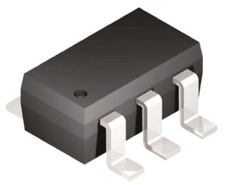
ICGOO电子元器件商城为您提供ADS1100A0IDBVT由Texas Instruments设计生产,在icgoo商城现货销售,并且可以通过原厂、代理商等渠道进行代购。 ADS1100A0IDBVT价格参考。Texas InstrumentsADS1100A0IDBVT封装/规格:数据采集 - 模数转换器, 16 Bit Analog to Digital Converter 1 Input 1 Sigma-Delta SOT-23-6。您可以下载ADS1100A0IDBVT参考资料、Datasheet数据手册功能说明书,资料中有ADS1100A0IDBVT 详细功能的应用电路图电压和使用方法及教程。
ADS1100A0IDBVT是德州仪器(Texas Instruments)推出的一款高精度、低功耗的16位模数转换器(ADC),属于数据采集类产品。该器件采用小型DBV封装(SOT-23-6),适用于对空间和功耗敏感的应用场景。

其典型应用场景包括便携式设备和电池供电系统,如手持式测量仪器、工业传感器信号调理模块以及医疗监测设备(如血糖仪、体温计等)。由于具备内置增益放大器(可编程增益达8V/V),它能够精确采集微弱模拟信号,适合用于桥式传感器(如压力传感器、称重传感器)的信号采集。

此外,ADS1100A0IDBVT支持I²C通信接口,便于与微控制器连接,广泛应用于工业自动化中的远程监控系统、环境监测设备(如温湿度、气体传感)以及智能楼宇控制系统中。其自校准功能和高信噪比特性确保了测量的准确性和稳定性。

综上,该芯片适用于需要高精度、小尺寸和低功耗的模拟信号采集场合,尤其适合在工业、医疗和消费类电子产品中实现可靠的传感器数据采集。
| 参数 | 数值 |
| 产品目录 | 集成电路 (IC)半导体 |
| 描述 | IC ADC 16-BIT I2C PROGBL SOT23-6模数转换器 - ADC Self-Calibrating 16-Bit |
| 产品分类 | |
| 品牌 | Texas Instruments |
| 产品手册 | http://www.ti.com/litv/sbas239b |
| 产品图片 |
|
| rohs | 符合RoHS无铅 / 符合限制有害物质指令(RoHS)规范要求 |
| 产品系列 | 数据转换器IC,模数转换器 - ADC,Texas Instruments ADS1100A0IDBVT- |
| 数据手册 | |
| 产品型号 | ADS1100A0IDBVT |
| 产品培训模块 | http://www.digikey.cn/PTM/IndividualPTM.page?site=cn&lang=zhs&ptm=13240 |
| 产品目录页面 | |
| 产品种类 | 模数转换器 - ADC |
| 位数 | 16 |
| 供应商器件封装 | SOT-23-6 |
| 信噪比 | Yes |
| 其它名称 | 296-12966-2 |
| 分辨率 | 16 bit |
| 制造商产品页 | http://www.ti.com/general/docs/suppproductinfo.tsp?distId=10&orderablePartNumber=ADS1100A0IDBVT |
| 包装 | Digi-Reel® |
| 商标 | Texas Instruments |
| 安装类型 | 表面贴装 |
| 安装风格 | SMD/SMT |
| 封装 | Reel |
| 封装/外壳 | SOT-23-6 |
| 封装/箱体 | SOT-23-6 |
| 工作温度 | -40°C ~ 85°C |
| 工作电源电压 | 2.7 V to 5.5 V |
| 工厂包装数量 | 250 |
| 接口类型 | Serial I2C |
| 数据接口 | I²C, 串行 |
| 最大功率耗散 | 0.75 mW |
| 最大工作温度 | + 85 C |
| 最小工作温度 | - 40 C |
| 标准包装 | 250 |
| 特性 | PGA |
| 电压参考 | 2.7 V to 5.5 V |
| 电压源 | 单电源 |
| 系列 | ADS1100 |
| 结构 | Sigma-Delta |
| 转换器数 | 1 |
| 转换器数量 | 1 |
| 转换速率 | 128 S/s |
| 输入数和类型 | 2 个单端,双极1 个差分,双极 |
| 输入类型 | Differential |
| 通道数量 | 1 Channel |
| 配用 | /product-detail/zh/ADS1100EVM/296-19903-ND/562100 |
| 采样率(每秒) | 8 ~ 128 |


- 商务部:美国ITC正式对集成电路等产品启动337调查
- 曝三星4nm工艺存在良率问题 高通将骁龙8 Gen1或转产台积电
- 太阳诱电将投资9.5亿元在常州建新厂生产MLCC 预计2023年完工
- 英特尔发布欧洲新工厂建设计划 深化IDM 2.0 战略
- 台积电先进制程称霸业界 有大客户加持明年业绩稳了
- 达到5530亿美元!SIA预计今年全球半导体销售额将创下新高
- 英特尔拟将自动驾驶子公司Mobileye上市 估值或超500亿美元
- 三星加码芯片和SET,合并消费电子和移动部门,撤换高东真等 CEO
- 三星电子宣布重大人事变动 还合并消费电子和移动部门
- 海关总署:前11个月进口集成电路产品价值2.52万亿元 增长14.8%


PDF Datasheet 数据手册内容提取
ADS1100 AD0 SBAS239B – MAY 2002 – REVISED NOVEMBER 2003 Self-Calibrating, 16-Bit ANALOG-TO-DIGITAL CONVERTER FEATURES DESCRIPTION (cid:1) COMPLETE DATA ACQUISITION SYSTEM IN A The ADS1100 is a precision, continuously self-calibrating TINY SOT23-6 PACKAGE Analog-to-Digital (A/D) converter with differential inputs and (cid:1) 16-BITS NO MISSING CODES up to 16 bits of resolution in a small SOT23-6 package. Conversions are performed ratiometrically, using the power (cid:1) INL: 0.0125% of FSR MAX supply as the reference voltage. The ADS1100 uses an (cid:1) CONTINUOUS SELF-CALIBRATION I2C-compatible serial interface and operates from a single (cid:1) SINGLE-CYCLE CONVERSION power supply ranging from 2.7V to 5.5V. The ADS1100 can perform conversions at rates of 8, 16, 32, (cid:1) PROGRAMMABLE GAIN AMPLIFIER or 128 samples per second. The onboard Programmable GAIN = 1, 2, 4, OR 8 Gain Amplifier (PGA), which offers gains of up to 8, allows (cid:1) LOW NOISE: 4µVp-p smaller signals to be measured with high resolution. In (cid:1) PROGRAMMABLE DATA RATE: 8SPS to 128SPS single-conversion mode, the ADS1100 automatically powers down after a conversion, greatly reducing current consump- (cid:1) INTERNAL SYSTEM CLOCK tion during idle periods. (cid:1) I2CTM INTERFACE The ADS1100 is designed for applications requiring high- (cid:1) POWER SUPPLY: 2.7V to 5.5V resolution measurement, where space and power consump- (cid:1) LOW CURRENT CONSUMPTION: 90µA tion are major considerations. Typical applications include portable instrumentation, industrial process control, and smart (cid:1) AVAILABLE IN EIGHT DIFFERENT ADDRESSES transmitters. APPLICATIONS A = 1, 2, 4, or 8 (cid:1) PORTABLE INSTRUMENTATION V SCL IN+ ∆Σ A/D I2C (cid:1) INDUSTRIAL PROCESS CONTROL PGA Converter Interface V SDA (cid:1) SMART TRANSMITTERS IN– (cid:1) CONSUMER GOODS VDD (cid:1) FACTORY AUTOMATION Clock GND (cid:1) TEMPERATURE MEASUREMENT Oscillator I2C is a registered trademark of Philips Incorporated. Please be aware that an important notice concerning availability, standard warranty, and use in critical applications of Texas Instruments semiconductor products and disclaimers thereto appears at the end of this data sheet. All trademarks are the property of their respective owners. PRODUCTION DATA information is current as of publication date. Copyright © 2002-2003, Texas Instruments Incorporated Products conform to specifications per the terms of Texas Instruments standard warranty. Production processing does not necessarily include testing of all parameters. www.ti.com
ABSOLUTE MAXIMUM RATINGS ELECTROSTATIC VDD to GND...........................................................................–0.3V to +6V DISCHARGE SENSITIVITY Input Current...............................................................100mA, Momentary Input Current.................................................................10mA, Continuous This integrated circuit can be damaged by ESD. Texas Voltage to GND, VIN+, VIN–..........................................................–0.3V to VDD + 0.3V Voltage to GND, SDA, SCL.....................................................–0.5V to 6V Instruments recommends that all integrated circuits be handled Maximum Junction Temperature...................................................+150°C with appropriate precautions. Failure to observe proper han- Operating Temperature..................................................–40°C to +125°C dling and installation procedures can cause damage. Storage Temperature......................................................–60°C to +150°C Lead Temperature (soldering, 10s) ...............................................+300°C ESD damage can range from subtle performance degrada- tion to complete device failure. Precision integrated circuits NOTE: (1) Stresses above those listed under “Absolute Maximum Ratings” may cause permanent damage to the device. Exposure to absolute maximum may be more susceptible to damage because very small conditions for extended periods may affect device reliability. parametric changes could cause the device not to meet its published specifications. PACKAGE/ORDERING INFORMATION SPECIFIED PACKAGE TEMPERATURE PACKAGE ORDERING TRANSPORT PRODUCT I2C ADDRESS PACKAGE-LEAD DESIGNATOR(1) RANGE MARKING NUMBER MEDIA, QUANTITY ADS1100 1001 000 SOT23-6 DBV –40°C to +85°C AD0 ADS1100A0IDBVT Tape and Reel, 250 " " " " " " ADS1100A0IDBVR Tape and Reel, 3000 ADS1100 1001 001 SOT23-6 DBV –40°C to +85°C AD1 ADS1100A1IDBVT Tape and Reel, 250 " " " " " " ADS1100A1IDBVR Tape and Reel, 3000 ADS1100 1001 010 SOT23-6 DBV –40°C to +85°C AD2 ADS1100A2IDBVT Tape and Reel, 250 " " " " " " ADS1100A2IDBVR Tape and Reel, 3000 ADS1100 1001 011 SOT23-6 DBV –40°C to +85°C AD3 ADS1100A3IDBVT Tape and Reel, 250 " " " " " " ADS1100A3IDBVR Tape and Reel, 3000 ADS1100 1001 100 SOT23-6 DBV –40°C to +85°C AD4 ADS1100A4IDBVT Tape and Reel, 250 " " " " " " ADS1100A4IDBVR Tape and Reel, 3000 ADS1100 1001 101 SOT23-6 DBV –40°C to +85°C AD5 ADS1100A5IDBVT Tape and Reel, 250 " " " " " " ADS1100A5IDBVR Tape and Reel, 3000 ADS1100 1001 110 SOT23-6 DBV –40°C to +85°C AD6 ADS1100A6IDBVT Tape and Reel, 250 " " " " " " ADS1100A6IDBVR Tape and Reel, 3000 ADS1100 1001 111 SOT23-6 DBV –40°C to +85°C AD7 ADS1100A7IDBVT Tape and Reel, 250 " " " " " " ADS1100A7IDBVR Tape and Reel, 3000 NOTE: (1) For the most current specifications and package information, refer to our web site at www.ti.com. PIN CONFIGURATION Top View SOT23 VIN– VDD SDA 6 5 4 AD0 1 2 3 V GND SCL IN+ NOTE: Marking text direction indicates pin 1. Marking text depends on I2C address; see ordering table. Marking for I2C address 1001000 shown. ADS1100 2 www.ti.com SBAS239B
ELECTRICAL CHARACTERISTICS All specifications at –40°C to +85°C, V = 5V, GND = 0V, and all PGAs, unless otherwise noted. DD ADS1100 PARAMETER CONDITIONS MIN TYP MAX UNITS ANALOG INPUT Full-Scale Input Voltage (V ) – (V ) ±V /PGA V IN+ IN– DD Analog Input Voltage V , V to GND GND – 0.2 V + 0.2 V IN+ IN– DD Differential Input Impedance 2.4/PGA MΩ Common-Mode Input Impedance 8 MΩ SYSTEM PERFORMANCE Resolution and No Missing Codes DR = 00 12 12 Bits DR = 01 14 14 Bits DR = 10 15 15 Bits DR = 11 16 16 Bits Conversion Rate DR = 00 104 128 184 SPS DR = 01 26 32 46 SPS DR = 10 13 16 23 SPS DR = 11 6.5 8 11.5 SPS Output Noise See Typical Characteristic Curves Integral Nonlinearity DR = 11, PGA = 1, End Point Fit(1) ±0.003 ±0.0125 % of FSR(2) Offset Error ±2.5/PGA ±5/PGA mV Offset Drift PGA = 1 1.5 8 µV/°C PGA = 2 1.0 4 µV/°C PGA = 4 0.7 2 µV/°C PGA = 8 0.6 2 µV/°C Gain Error 0.01 0.1 % Gain Error Drift 2 ppm/°C Common-Mode Rejection At DC, PGA = 8 94 100 dB At DC, PGA = 1 85 dB DIGITAL INPUT/OUTPUT Logic Level V 0.7 • V 6 V IH DD V GND – 0.5 0.3 • V V IL DD V I = 3mA GND 0.4 V OL OL Input Leakage I V = 5.5V 10 µA IH IH I V = GND –10 µA IL IL POWER-SUPPLY REQUIREMENTS Power-Supply Voltage V 2.7 5.5 V DD Supply Current Power Down 0.05 2 µA Active Mode 90 150 µA Power Dissipation V = 5.0V 450 750 µW DD V = 3.0V 210 µW DD NOTES: (1) 99% of full-scale. (2) FSR = Full-Scale Range = 2 • V /PGA. DD ADS1100 3 SBAS239B www.ti.com
TYPICAL CHARACTERISTICS At T = 25°C and V = 5V, unless otherwise noted. A DD SUPPLY CURRENT vs TEMPERATURE SUPPLY CURRENT vs I2C BUS FREQUENCY 120 250 225 V = 5V 100 DD 200 25°C 175 µI (A)VDD 80 µI (A)VDD 115205 125°C 60 100 VDD = 2.7V –40°C 75 40 50 –60 –40 –20 0 20 40 60 80 100 120 140 10 100 1k 10k Temperature (°C) I2C Bus Frequency (kHz) OFFSET ERROR vs TEMPERATURE OFFSET ERROR vs TEMPERATURE 2.0 2.0 V = 5V V = 2.7V DD DD 1.0 1.0 V) PGA = 8 PGA = 4 PGA = 2 PGA = 1 V) PGA = 8 PGA = 4 PGA = 2 PGA = 1 m m or ( or ( Err 0.0 Err 0.0 et et s s Off Off –1.0 –1.0 –2.0 –2.0 –60 –40 –20 0 20 40 60 80 100 120 140 –60 –40 –20 0 20 40 60 80 100 120 140 Temperature (°C) Temperature (°C) GAIN ERROR vs TEMPERATURE GAIN ERROR vs TEMPERATURE 0.04 0.010 0.03 VDD = 5V VDD = 2.7V 0.005 PGA = 8 PGA = 4 PGA = 4 0.02 PGA = 1 PGA = 8 %) 0.01 %) 0.000 or ( or ( Err 0.00 Err –0.005 n n ai –0.01 ai PGA = 1 G G –0.010 PGA = 2 –0.02 PGA = 2 –0.015 –0.03 –0.04 –0.020 –60 –40 –20 0 20 40 60 80 100 120 140 –60 –40 –20 0 20 40 60 80 100 120 140 Temperature (°C) Temperature (°C) ADS1100 4 www.ti.com SBAS239B
TYPICAL CHARACTERISTICS (Cont.) At T = 25°C and V = 5V, unless otherwise noted. A DD TOTAL ERROR vs INPUT SIGNAL INTEGRAL NONLINEARITY vs SUPPLY VOLTAGE 0.0 0.016 PGA = 8 PGA = 8 R) 0.014 PGA = 4 –0.5 S PGA = 2 F 0.012 PGA = 4 of PGA = 1 Error (mV) –1.0 PGA = 2 nearity (% 00..001008 al –1.5 nli 0.006 Tot No al 0.004 –2.0 gr e nt 0.002 PGA = 1 Data Rate = 8SPS I –2.5 0.000 –100 –75 –50 –25 0 25 50 75 100 2.5 3.0 3.5 4.0 4.5 5.0 5.5 Input Signal (% of Full-Scale) V (V) DD INTEGRAL NONLINEARITY vs TEMPERATURE NOISE vs INPUT SIGNAL 0.05 20 PGA =1 Data Rate = 8SPS R) PGA = 8 FS 0.04 % of LSB) 15 PGA = 4 y ( 0.03 of egral Nonlinearit 00..0021 VDD = V3D.5DV = 2.7V VDD = 5V Noise (p-p, % 105 PPGGAA == 21 nt I 0.00 0 –60 –40 –20 0 20 40 60 80 100 120 140 0 20 40 60 80 100 Temperature (°C) Input Signal (% of Full-Scale) NOISE vs SUPPLY VOLTAGE NOISE vs TEMPERATURE 30 25 Data Rate = 8SPS PGA = 8 25 B) PGA = 8 B) 20 % of LS 20 PGA = 4 % of LS Noise (p-p, 1150 PGA = 2 Noise (p-p, 1150 5 Data Rate = 8SPS PGA = 1 0 5 2.5 3.0 3.5 4.0 4.5 5.0 5.5 –60 –40 –20 0 20 40 60 80 100 120 140 V (V) Temperature (°C) DD ADS1100 5 SBAS239B www.ti.com
TYPICAL CHARACTERISTICS (Cont.) At T = 25°C and V = 5V, unless otherwise noted. A DD DATA RATE vs TEMPERATURE FREQUENCY RESPONSE 10 0 Data Rate = 8SPS VDD = 2.7V –20 9 S) P ate (S 8 n (dB) –40 a R Gai –60 Dat VDD = 5V 7 –80 Data Rate = 8SPS 6 –100 –60 –40 –20 0 20 40 60 80 100 120 140 0.1 1 10 100 1k Temperature (°C) Input Frequency (Hz) THEORY OF OPERATION For a minimum output code of Min Code, gain setting of PGA, positive and negative input voltages of V and V , IN+ IN– The ADS1100 is a fully differential, 16-bit, self-calibrating, and power supply of V , the output code is given by the DD delta-sigma A/D converter. Extremely easy to design with expression: and configure, the ADS1100 allows you to obtain precise ( ) ( ) measurements with a minimum of effort. V – V Output Code=–1•Min Code•PGA• IN+ IN– The ADS1100 consists of a delta-sigma A/D converter core with V DD adjustable gain, a clock generator, and an I2C interface. Each of In the previous expression, it is important to note that the negated these blocks are described in detail in the sections that follow. minimum output code is used. The ADS1100 outputs codes in binary two’s complement format, so the absolute values of the ANALOG-TO-DIGITAL CONVERTER minima and maxima are not the same; the maximum n-bit code The ADS1100 A/D converter core consists of a differential is 2n-1 – 1, while the minimum n-bit code is –1 • 2n-1. switched-capacitor delta-sigma modulator followed by a digital For example, the ideal expression for output codes with a filter. The modulator measures the voltage difference between data rate of 16SPS and PGA = 2 is: the positive and negative analog inputs and compares it to a ( ) ( ) reference voltage, which, in the ADS1100, is the power V – V supply. The digital filter receives a high-speed bitstream from Output Code=16384•2• IN+ IN– V the modulator and outputs a code, which is a number DD proportional to the input voltage. The ADS1100 outputs all codes right-justified and sign- extended. This makes it possible to perform averaging on the OUTPUT CODE CALCULATION higher data rate codes using only a 16-bit accumulator. The output code is a scalar value that is (except for clipping) See Table II for output codes for various input levels. proportional to the voltage difference between the two analog inputs. The output code is confined to a finite range of numbers; SELF-CALIBRATION this range depends on the number of bits needed to represent the code. The number of bits needed to represent the output code for The previous expressions for the ADS1100’s output code do the ADS1100 depends on the data rate, as shown in Table I. not account for the gain and offset errors in the modulator. To compensate for these, the ADS1100 incorporates self-cali- bration circuitry. DATA RATE NUMBER OF BITS MINIMUM CODE MAXIMUM CODE The self-calibration system operates continuously, and re- 8SPS 16 –32,768 32,767 quires no user intervention. No adjustments can be made to 16SPS 15 –16,384 16,383 the self-calibration system, and none need to be made. The 32SPS 14 –8192 8191 128SPS 12 –2048 2047 self-calibration system cannot be deactivated. TABLE I. Minimum and Maximum Codes. The offset and gain error figures shown in the Electrical Characteristics include the effects of calibration. ADS1100 6 www.ti.com SBAS239B
INPUT SIGNAL DATA RATE NEGATIVE FULL-SCALE –1LSB ZERO +1LSB POSITIVE FULL-SCALE 8SPS 8000 FFFF 0000 0001 7FFF H H H H H 16SPS C000 FFFF 0000 0001 3FFF H H H H H 32SPS E000 FFFF 0000 0001 1FFF H H H H H 128SPS F800 FFFF 0000 0001 07FF H H H H H TABLE II. Output Codes for Different Input Signals. CLOCK GENERATOR When designing an input filter circuit, remember to take into The ADS1100 features an onboard clock generator, which account the interaction between the filter network and the input impedance of the ADS1100. drives the operation of the modulator and digital filter. The Typical Characteristics show varieties in data rate over supply voltage and temperature. USING THE ADS1100 It is not possible to operate the ADS1100 with an external modulator clock. OPERATING MODES The ADS1100 operates in one of two modes: continuous INPUT IMPEDANCE conversion and single conversion. The ADS1100 uses a switched-capacitor input stage. To In continuous conversion mode, the ADS1100 continuously external circuitry, it looks roughly like a resistance. The performs conversions. Once a conversion has been com- resistance value depends on the capacitor values and the pleted, the ADS1100 places the result in the output register, rate at which they are switched. The switching frequency is and immediately begins another conversion. When the the same as the modulator frequency; the capacitor values ADS1100 is in continuous conversion mode, the ST/BSY bit depend on the PGA setting. The switching clock is generated in the configuration register always reads 1. by the onboard clock generator, so its frequency, nominally In single conversion mode, the ADS1100 waits until the 275kHz, is dependent on supply voltage and temperature. ST/BSY bit in the conversion register is set to 1. When this The common-mode and differential input impedances are happens, the ADS1100 powers up and performs a single different. For a gain setting of PGA, the differential input conversion. After the conversion completes, the ADS1100 impedance is typically: places the result in the output register, resets the ST/BSY bit to 0 and powers down. Writing a 1 to ST/BSY while a 2.4MΩ/PGA conversion is in progress has no effect. The common-mode impedance is typically 8MΩ. When switching from continuous conversion mode to single The typical value of the input impedance often cannot be conversion mode, the ADS1100 will complete the current neglected. Unless the input source has a low impedance, the conversion, reset the ST/BSY bit to 0 and power down. ADS1100’s input impedance may affect the measurement accu- racy. For sources with high output impedance, buffering may be RESET AND POWER-UP necessary. Bear in mind, however, that active buffers introduce When the ADS1100 powers up, it automatically performs a noise, and also introduce offset and gain errors. All of these reset. As part of the reset, the ADS1100 sets all of the bits factors should be considered in high-accuracy applications. in the configuration register to their default setting. Because the clock generator frequency drifts slightly with The ADS1100 responds to the I2C General Call Reset temperature, the input impedances will also drift. For many command. When the ADS1100 receives a General Call applications, this input impedance drift can be neglected, and Reset, it performs an internal reset, exactly as though it had the typical impedance values above can be used. just been powered on. ALIASING I2C INTERFACE If frequencies are input to the ADS1100 that exceed half the The ADS1100 communicates through an I2C (Inter-Inte- data rate, aliasing will occur. To prevent aliasing, the input grated Circuit) interface. The I2C interface is a 2-wire open- signal must be bandlimited. Some signals are inherently drain interface supporting multiple devices and masters on a bandlimited. For example, a thermocouple’s output, which single bus. Devices on the I2C bus only drive the bus lines has a limited rate of change, may nevertheless contain noise LOW, by connecting them to ground; they never drive the and interference components. These can fold back into the bus lines HIGH. Instead, the bus wires are pulled HIGH by sampling band just as any other signal can. pull-up resistors, so the bus wires are HIGH when no device The ADS1100’s digital filter provides some attenuation of is driving them LOW. This way, two devices cannot conflict; high-frequency noise, but the filter’s sinc1 frequency re- if two devices drive the bus simultaneously, there is no driver sponse cannot completely replace an anti-aliasing filter; contention. some external filtering may still be needed. For many appli- cations, a simple RC filter will suffice. ADS1100 7 SBAS239B www.ti.com
Communication on the I2C bus always takes place between Every byte transmitted on the I2C bus, whether it be address two devices, one acting as the master and the other acting or data, is acknowledged with an acknowledge bit. When a as the slave. Both masters and slaves can read and write, master has finished sending a byte, eight data bits, to a but slaves can only do so under the direction of the master. slave, it stops driving SDA and waits for the slave to acknowl- Some I2C devices can act as masters or slaves, but the edge the byte. The slave acknowledges the byte by pulling ADS1100 can only act as a slave device. SDA LOW. The master then sends a clock pulse to clock the An I2C bus consists of two lines, SDA and SCL. SDA carries acknowledge bit. Similarly, when a master has finished reading a byte, it pulls SDA LOW to acknowledge this to the data; SCL provides the clock. All data is transmitted across the I2C bus in groups of eight bits. To send a bit on the I2C slave. It then sends a clock pulse to clock the bit. (Remember that the master always drives the clock line.) bus, the SDA line is driven to the bit’s level while SCL is LOW (a LOW on SDA indicates the bit is zero; a HIGH indicates A not-acknowledge is performed by simply leaving SDA the bit is one). Once the SDA line has settled, the SCL line HIGH during an acknowledge cycle. If a device is not present is brought HIGH, then LOW. This pulse on SCL clocks the on the bus, and the master attempts to address it, it will SDA bit into the receiver’s shift register. receive a not-acknowledge because no device is present at The I2C bus is bidirectional: the SDA line is used both for that address to pull the line LOW. transmitting and receiving data. When a master reads from When a master has finished communicating with a slave, it a slave, the slave drives the data line; when a master sends may issue a stop condition. When a stop condition is issued, to a slave, the master drives the data line. The master always the bus becomes idle again. A master may also issue drives the clock line. The ADS1100 never drives SCL, another start condition. When a start condition is issued while because it cannot act as a master. On the ADS1100, SCL is the bus is active, it is called a repeated start condition. an input only. A timing diagram for an ADS1100 I2C transaction is shown in Most of the time the bus is idle, no communication is taking Figure 1. Table III gives the parameters for this diagram. place, and both lines are HIGH. When communication is taking place, the bus is active. Only master devices can start ADS1100 I2C ADDRESSES a communication. They do this by causing a start condition The ADS1100 I2C address is 1001aaa, where “aaa” are bits on the bus. Normally, the data line is only allowed to change set at the factory. The ADS1100 is available in eight different state while the clock line is LOW. If the data line changes verisons, each having a different I2C address. For example, state while the clock line is HIGH, it is either a start condition the ADS1100A0 has address 1001000, and the ADS1100A3 or its counterpart, a stop condition. A start condition is when has address 1001011. See the Package/Ordering Informa- the clock line is HIGH and the data line goes from HIGH to tion table for a complete listing. LOW. A stop condition is when the clock line is HIGH and the data line goes from LOW to HIGH. The I2C address is the only difference between the eight variants. In all other repsects, they operate identically. After the master issues a start condition, it sends a byte that indicates which slave device it wants to communicate with. Each variant of the ADS1100 is marked with “ADx,” where x This byte is called the address byte. Each device on an I2C identifies the address variant. For example, the ADS1100A0 is marked “AD0”, and the ADS1100A3 is marked “AD3”. See the bus has a unique 7-bit address to which it responds. (Slaves can also have 10-bit addresses; see the I2C specification for Package/Ordering Information table for a complete listing. details.) The master sends an address in the address byte, When the ADS1100 was first introduced, it was shipped with together with a bit that indicates whether it wishes to read only one address, 1001000, and was marked “BAAI.” That from or write to the slave device. device is identical to the currently shipping ADS1100A0 variant marked “AD0”. t (LOW) tR tF t(HDSTA) SCL t(HDSTA) t(HIGH) t(SUSTA) t(SUSTO) t t (HDDAT) (SUDAT) SDA t (BUF) P S S P FIGURE 1. I2C Timing Diagram. ADS1100 8 www.ti.com SBAS239B
FAST MODE HIGH-SPEED MODE PARAMETER MIN MAX MIN MAX UNITS SCLK Operating Frequency f 0.4 3.4 MHz (SCLK) Bus Free Time Between STOP and START Condition t 600 160 ns (BUF) Hold Time After Repeated START Condition. t 600 160 ns (HDSTA) After this period, the first clock is generated. Repeated START Condition Setup Time t 600 160 ns (SUSTA) STOP Condition Setup Time t 600 160 ns (SUSTO) Data Hold Time t 0 0 ns (HDDAT) Data Setup Time t 100 10 ns (SUDAT) SCLK Clock LOW Period t 1300 160 ns (LOW) SCLK Clock HIGH Period t 600 60 ns (HIGH) Clock/Data Fall Time t 300 160 ns F Clock/Data Rise Time t 300 160 ns R TABLE III. Timing Diagram Definitions. I2C GENERAL CALL REGISTERS The ADS1100 responds to General Call Reset, which is an The ADS1100 has two registers that are accessible via its I2C address byte of 00 followed by a data byte of 06 . The port. The output register contains the result of the last conver- H H ADS1100 acknowledges both bytes. sion; the configuration register allows you to change the ADS1100’s operating mode and query the status of the device. On receiving a General Call Reset, the ADS1100 performs a full internal reset, just as though it had been powered off and then on. If a conversion is in process, it is interrupted; the OUTPUT REGISTER output register is set to zero, and the configuration register is The 16-bit output register contains the result of the last set to its default setting. conversion in binary two’s complement format. Following The ADS1100 always acknowledges the General Call ad- reset or power-up, the output register is cleared to zero; it dress byte of 00 , but it does not acknowledge any General remains zero until the first conversion is completed. There- H Call data bytes other than 04 or 06 . fore, if you read the ADS1100 just after reset or power-up, H H you will read zero from the output register. I2C DATA RATES The output register’s format is shown in Table IV. The I2C bus operates in one of three speed modes: Stan- dard, which allows a clock frequency of up to 100kHz; Fast, CONFIGURATION REGISTER which allows a clock frequency of up to 400kHz; and High- You can use the 8-bit configuration register to control the speed mode (also called Hs mode), which allows a clock ADS1100’s operating mode, data rate, and PGA settings. frequency of up to 3.4MHz. The ADS1100 is fully compatible The configuration register’s format is shown in Table V. The with all three modes. default setting is 8CH. No special action needs to be taken to use the ADS1100 in Standard or Fast modes, but High-speed mode must be BIT 7 6 5 4 3 2 1 0 activated. To activate High-speed mode, send a special NAME ST/BSY 0 0 SC DR1 DR0 PGA1 PGA0 address byte of 00001XXX following the start condition, where the XXX bits are unique to the Hs-capable master. TABLE V. Configuration Register. This byte is called the Hs master code. (Note that this is different from normal address bytes: the low bit does not Bit 7: ST/BSY indicate read/write status.) The ADS1100 will not acknowl- The meaning of the ST/BSY bit depends on whether it is edge this byte; the I2C specification prohibits acknowledg- being written to or read from. ment of the Hs master code. On receiving a master code, the In single conversion mode, writing a 1 to the ST/BSY bit ADS1100 will switch on its High-speed mode filters, and will causes a conversion to start, and writing a 0 has no effect. communicate at up to 3.4MHz. The ADS1100 switches out of In continuous conversion mode, the ADS1100 ignores the Hs mode with the next stop condition. value written to ST/BSY. For more information on High-speed mode, consult the I2C specification. BIT 15 14 13 12 11 10 9 8 7 6 5 4 3 2 1 0 NAME D15 D14 D13 D12 D11 D10 D9 D8 D7 D6 D5 D4 D3 D2 D1 D0 TABLE IV. Output Register. ADS1100 9 SBAS239B www.ti.com
When read in single conversion mode, ST/BSY indicates whether READING FROM THE ADS1100 the A/D converter is busy taking a conversion. If ST/BSY is read You can read the output register and the contents of the as 1, the A/D converter is busy, and a conversion is taking configuration register from the ADS1100. To do this, address place; if 0, no conversion is taking place, and the result of the the ADS1100 for reading, and read three bytes from the last conversion is available in the output register. device. The first two bytes are the output register’s contents; In continuous mode, ST/BSY is always read as 1. the third byte is the configuration register’s contents. Bits 6-5: Reserved You do not always have to read three bytes from the ADS1100. If you want only the contents of the output regis- Bits 6 and 5 must be set to zero. ter, read only two bytes. Bit 4: SC Reading more than three bytes from the ADS1100 has no SC controls whether the ADS1100 is in continuous conver- effect. All of the bytes beginning with the fourth will be FF . sion or single conversion mode. When SC is 1, the ADS1100 H is in single conversion mode; when SC is 0, the ADS1100 is See Figure 2 for a timing diagram of an ADS1100 read in continuous conversion mode. The default setting is 0. operation. Bits 3-2: DR WRITING TO THE ADS1100 Bits 3 and 2 control the ADS1100’s data rate, as shown in Table VI. You can write new contents into the configuration register (you cannot change the contents of the output register). To do this, address the ADS1100 for writing, and write one byte DR1 DR0 DATA RATE to it. This byte is written into the configuration register. 0 0 128SPS Writing more than one byte to the ADS1100 has no effect. 0 1 32SPS 1 0 16SPS The ADS1100 will ignore any bytes sent to it after the first 1(1) 1(1) 8SPS(1) one, and it will only acknowledge the first byte. NOTE: (1) Default Setting. See Figure 3 for a timing diagram of an ADS1100 write TABLE VI. DR Bits. operation. Bits 1-0: PGA Bits 1 and 0 control the ADS1100’s gain setting, as shown in Table VII. PGA1 PGA0 GAIN 0(1) 0(1) 1(1) 0 1 2 1 0 4 1 1 8 NOTE: (1) Default Setting. TABLE VII. PGA Bits. ADS1100 10 www.ti.com SBAS239B
1 9 1 9 SCL … SDA … 1 0 0 1 A2 A1 A0 R/W D15 D14 D13 D12 D11 D10 D9 D8 Start By ACK By From ACK By Master ADS1100 ADS1100 Master Frame 1: I2C Slave Address Byte Frame 2: Output Register Upper Byte 1 9 1 9 SCL … (Continued) SDA … ST/ D7 D6 D5 D4 D3 D2 D1 D0 0 0 SC DR1 DR0 PGA1 PGA0 (Continued) BSY From ACK By From ACK By Stop By ADS1100 Master ADS1100 Master Master Frame 3: Output Register Lower Byte Frame 4: Configuration Register (Optional) FIGURE 2. Timing Diagram for Reading From the ADS1100. 1 9 1 9 SCL ST/ SDA 1 0 0 1 A2 A1 A0 R/W 0 0 SC DR1 DR0 PGA1 PGA0 Stop By BSY Master Start By ACK By ACK By Master ADS1100 ADS1100 Frame 1: I2C Slave Address Byte Frame 2: Configuration Register FIGURE 3. Timing Diagram for Writing to the ADS1100. ADS1100 11 SBAS239B www.ti.com
APPLICATIONS INFORMATION non-multiiple-master I2C peripherals, will work with the ADS1100. The ADS1100 does not perform clock-stretching The sections that follow give example circuits and tips for (i.e., it never pulls the clock line low), so it is not necessary using the ADS1100 in various situations. to provide for this unless other devices are on the same I2C An evaluation board, the ADS1100EVM, is available. This bus. small, simple board connects to an RS-232 serial port on Pull-up resistors are necessary on both the SDA and SCL almost any PC. The supplied software simulates a digital lines because I2C bus drivers are open-drain. The size of voltmeter, and also displays raw output codes in hex and these resistors depends on the bus operating speed and decimal. All features of the ADS1100 can be controlled from capacitance of the bus lines. Higher-value resistors consume the main window. For more information, contact TI or your less power, but increase the transition times on the bus, local TI representative, or visit the Texas Instruments website limiting the bus speed. Lower-value resistors allow higher at http://www.ti.com/. speed at the expense of higher power consumption. Long bus lines have higher capacitance and require smaller pull- BASIC CONNECTIONS up resistors to compensate. The resistors should not be too small; if they are, the bus drivers may not be able to pull the For many applications, connecting the ADS1100 is extremely bus lines low. simple. A basic connection diagram for the ADS1100 is shown in Figure 4. CONNECTING MULTIPLE DEVICES The fully differential voltage input of the ADS1100 is ideal for connection to differential sources with moderately low source Connecting multiple ADS1100s to a single bus is almost impedance, such as bridge sensors and thermistors. Al- trivial. The ADS1100 is available in eight different ver- though the ADS1100 can read bipolar differential signals, it sions, each of which has a different I2C address. An cannot accept negative voltages on either input. It may be example showing three ADS1100s connected on a single helpful to think of the ADS1100 positive voltage input as non- bus is shown in Figure 5. Up to eight ADS1100s (provided inverting, and of the negative input as inverting. their addresses are different) can be connected to a single When the ADS1100 is converting, it draws current in short bus. spikes. The 0.1µF bypass capacitor supplies the momentary Note that only one set of pull-up resistors is needed per bus. bursts of extra current needed from the supply. You might find that you need to lower the pull-up resistor The ADS1100 interfaces directly to standard mode, fast values slightly to compensate for the additional bus capaci- mode, and high-speed mode I2C controllers. Any tance presented by multiple devices and increased line microcontroller’s I2C peripheral, including master-only and length. Positive Input Negative Input (0V to 5V) (0V to 5V) I2C Pull-Up Resistors V 1kΩ to 10kΩ (typ.) DD ADS1100 V DD Microcontroller or 1 VIN+ VIN– 6 Microprocessor with I2C Port 2 GND VDD 5 SCL 3 SCL SDA 4 4.7µF (typ.) SDA FIGURE 4. Typical Connections of the ADS1100. ADS1100 12 www.ti.com SBAS239B
Note that no pull-up resistor is shown on the SCL line. In this I2C Pull-Up Resistors 1kΩ to 10kΩ (typ.) VDD simple case, the resistor is not needed; the microcontroller can simply leave the line on output, and set it to one or zero ADS1100A0 as appropriate. It can do this because the ADS1100 never Microcontroller or 1 VIN+ VIN– 6 drives its clock line low. This technique can also be used with Microprocessor with I2C Port 2 GND VDD 5 multiple devices, and has the advantage of lower current consumption due to the absence of a resistive pull-up. SCL 3 SCL SDA 4 If there are any devices on the bus that may drive their clock SDA lines low, the above method should not be used; the SCL line should be high-Z or zero and a pull-up resistor provided as ADS1100A1 usual. Note also that this cannot be done on the SDA line in 1 VIN+ VIN– 6 any case, because the ADS1100 does drive the SDA line low 2 GND VDD 5 from time to time, as all I2C devices do. Some microcontrollers have selectable strong pull-up circuits 3 SCL SDA 4 built in to their GPIO ports. In some cases, these can be switched on and used in place of an external pull-up resistor. Weak pull-ups are also provided on some microcontrollers, NOTE: ADS1100 power ADS1100A2 but usually these are too weak for I2C communication. If aonmdit tiendp ufot rc ocnlanreityc.tions 1 VIN+ VIN– 6 there is any doubt about the matter, test the circuit before 2 GND VDD 5 committing it to production. 3 SCL SDA 4 SINGLE-ENDED INPUTS Although the ADS1100 has a fully differential input, it can FIGURE 5. Connecting Multiple ADS1100s. easily measure single-ended signals. A simple single-ended connection scheme is shown in Figure 7. The ADS1100 is USING GPIO PORTS FOR I2C configured for single-ended measurement by grounding ei- ther of its input pins, usually V –, and applying the input Most microcontrollers have programmable input/output pins IN signal to V +. The single-ended signal can range from –0.2V that can be set in software to act as inputs or outputs. If an IN to V + 0.3V. The ADS1100 loses no linearity anywhere in I2C controller is not available, the ADS1100 can be con- DD its input range. Negative voltages cannot be applied to this nected to GPIO pins, and the I2C bus protocol simulated, or circuit because the ADS1100 inputs can only accept positive bit-banged, in software. An example of this for a single voltages. ADS1100 is shown in Figure 6. V DD ADS1100 Microcontroller or 1 VIN+ VIN– 6 VDD Microprocessor with I2C Port 2 GND VDD 5 0V - V DD ADS1100 Single-Ended SCL 3 SCL SDA 4 1 VIN+ VIN– 6 SDA 2 GND VDD 5 Filter Capacitor 3 SCL SDA 4 Output NOTE: ADS1100 power 33pF to 100pF Codes and input connections (typ.) 0-32767 omitted for clarity. FIGURE 6. Using GPIO with a Single ADS1100. FIGURE 7. Measuring Single-Ended Inputs. Bit-banging I2C with GPIO pins can be done by setting the The ADS1100 input range is bipolar differential with respect GPIO line to zero and toggling it between input and output to the reference, i.e. ±V . The single-ended circuit shown in DD modes to apply the proper bus states. To drive the line low, Figure 7 covers only half the ADS1100 input scale because the pin is set to output a zero; to let the line go high, the pin it does not produce differentially negative inputs; therefore, is set to input. When the pin is set to input, the state of the one bit of resolution is lost. The Burr-Brown DRV134 bal- pin can be read; if another device is pulling the line low, this anced line driver from Texas Instruments can be employed will read as a zero in the port’s input register. to regain this bit for single-ended signals. ADS1100 13 SBAS239B www.ti.com
Negative input voltages must be level-shifted. A good candi- WHEATSTONE BRIDGE SENSOR date for this function is the Texas Instruments THS4130 The ADS1100 has a fully differential high-impedance input differential amplifier, which can output fully differential sig- stage and internal gain circuitry, which makes it a good nals. This device can also help recover the lost bit noted candidate for bridge-sensor measurement. An example is previously for single-ended positive signals. Level shifting shown in Figure 9. can also be performed using the DRV134. LOW-SIDE CURRENT MONITOR V DD Figure 8 shows a circuit for a low-side shunt-type current Bridge monitor. The circuit reads the voltage across a shunt resistor, Sensor E+ which is sized as small as possible while still giving a readable output voltage. This voltage is amplified by an OPA335 low- drift op-amp, and the result is read by the ADS1100. V– V+ E– 11.5kΩ V 5V 5V ADS1100 V DD 1 VIN+ VIN– 6 FS = 0.63V Load OPA335 2 GND VDD 5 R493.(19)kΩ ADS1100 I2C 3 SCL SDA 4 4.7µF R (2) 1kΩ S G = 12.5 –5V (PGA Gain = 8) 5V FS NOTE: (1) Pull-down resistor to allow accurate swing to 0V. I2C I/O (2) R is sized for a 50mV drop at full-scale current. S FIGURE 9. Measuring a Wheatstone Bridge Sensor. FIGURE 8. Low-Side Current Measurement. The Wheatstone bridge sensor is connected directly to the ADS1100 without intervening instrumentation amplifiers; a It is suggested that the ADS1100 be operated at a gain of 8. The single, small input capacitor provides rejection of high-fre- gain of the OPA335 can then be set lower. For a gain of 8, the quency interference. The excitation voltage of the bridge is op amp should be set up to give a maximum output voltage of the power supply, which is also the ADS1100 reference no greater than 0.75V. If the shunt resistor is sized to provide voltage. The measurement is, therefore, ratiometric. In this a maximum voltage drop of 50mV at full-scale current, the circuit, the ADS1100 would typically be operated at a gain of full-scale input to the ADS1100 is 0.63V. 8. The input range in this case is ±0.75 volts. ADS1100 14 www.ti.com SBAS239B
Many resistive bridge sensors, such as strain gauges, have If the ADS1100 is driven by an op amp with high voltage very small full-scale output ranges. For these sensors, the supplies, such as ±12V, protection should be provided, even measurement resolution obtainable without additional ampli- if the op amp is configured so that it will not output out-of- fication can be low. For example, if the bridge sensor output range voltages. Many op amps seek to one of the supply rails is ±20mV, the ADS1100 outputs codes from approximately immediately when power is applied, usually before the input –873 to +873, resulting in a best-case resolution of around 11 has stabilized; this momentary spike can damage the ADS1100. bits. If higher resolution is required, it is best to supply an Sometimes this damage is incremental and results in slow, external instrumentation amplifier to bring the signal to full long-term failure—which can be distastrous for permanently scale. installed, low-maintenance systems. If you use an op amp or other front-end circuitry with the ADVICE ADS1100, be sure to take the performance characteristics of this circuitry into account. A chain is only as strong as its weakest link. The ADS1100 is fabricated in a small-geometry low-voltage process. The analog inputs feature protection diodes to the supply rails. However, the current-handling ability of these LAYOUT TIPS diodes is limited, and the ADS1100 can be permanently PCB layout for the ADS1100 is relatively undemanding. damaged by analog input voltages that remain more than 16-bit performance is not difficult to achieve. approximately 300mV beyond the rails for extended periods. Any data converter is only as good as its reference. For the One way to protect against overvoltage is to place current- ADS1100, the reference is the power supply, and the power limiting resistors on the input lines. The ADS1100 analog supply must be clean enough to achieve the desired perfor- inputs can withstand momentary currents of as large as mance. If a power-supply filter capacitor is used, it should be 10mA. placed close to the V pin, with no vias placed between the DD The previous paragraph does not apply to the I2C ports, capacitor and the pin. The trace leading to the pin should be as which can both be driven to 6V regardless of the supply. wide as possible, even if it must be necked down at the device. ADS1100 15 SBAS239B www.ti.com
PACKAGE OPTION ADDENDUM www.ti.com 14-Sep-2018 PACKAGING INFORMATION Orderable Device Status Package Type Package Pins Package Eco Plan Lead/Ball Finish MSL Peak Temp Op Temp (°C) Device Marking Samples (1) Drawing Qty (2) (6) (3) (4/5) ADS1100A0IDBVR ACTIVE SOT-23 DBV 6 3000 Green (RoHS CU NIPDAU Level-1-260C-UNLIM -40 to 85 AD0 & no Sb/Br) ADS1100A0IDBVRG4 ACTIVE SOT-23 DBV 6 3000 Green (RoHS CU NIPDAU Level-1-260C-UNLIM -40 to 85 AD0 & no Sb/Br) ADS1100A0IDBVT ACTIVE SOT-23 DBV 6 250 Green (RoHS CU NIPDAU Level-1-260C-UNLIM -40 to 85 AD0 & no Sb/Br) ADS1100A0IDBVTG4 ACTIVE SOT-23 DBV 6 250 Green (RoHS CU NIPDAU Level-1-260C-UNLIM -40 to 85 AD0 & no Sb/Br) ADS1100A1IDBVR ACTIVE SOT-23 DBV 6 3000 Green (RoHS CU NIPDAU Level-1-260C-UNLIM -40 to 85 AD1 & no Sb/Br) ADS1100A1IDBVT ACTIVE SOT-23 DBV 6 250 Green (RoHS CU NIPDAU Level-1-260C-UNLIM -40 to 85 AD1 & no Sb/Br) ADS1100A1IDBVTG4 ACTIVE SOT-23 DBV 6 250 Green (RoHS CU NIPDAU Level-1-260C-UNLIM -40 to 85 AD1 & no Sb/Br) ADS1100A2IDBVR ACTIVE SOT-23 DBV 6 3000 Green (RoHS CU NIPDAU Level-1-260C-UNLIM -40 to 85 AD2 & no Sb/Br) ADS1100A2IDBVT ACTIVE SOT-23 DBV 6 250 Green (RoHS CU NIPDAU Level-1-260C-UNLIM -40 to 85 AD2 & no Sb/Br) ADS1100A2IDBVTG4 ACTIVE SOT-23 DBV 6 250 Green (RoHS CU NIPDAU Level-1-260C-UNLIM -40 to 85 AD2 & no Sb/Br) ADS1100A3IDBVT ACTIVE SOT-23 DBV 6 250 Green (RoHS CU NIPDAU Level-1-260C-UNLIM -40 to 85 AD3 & no Sb/Br) ADS1100A3IDBVTG4 ACTIVE SOT-23 DBV 6 250 Green (RoHS CU NIPDAU Level-1-260C-UNLIM -40 to 85 AD3 & no Sb/Br) ADS1100A4IDBVR ACTIVE SOT-23 DBV 6 3000 Green (RoHS CU NIPDAU Level-1-260C-UNLIM -40 to 85 AD4 & no Sb/Br) ADS1100A4IDBVRG4 ACTIVE SOT-23 DBV 6 3000 Green (RoHS CU NIPDAU Level-1-260C-UNLIM -40 to 85 AD4 & no Sb/Br) ADS1100A4IDBVT ACTIVE SOT-23 DBV 6 250 Green (RoHS CU NIPDAU Level-1-260C-UNLIM -40 to 85 AD4 & no Sb/Br) ADS1100A5IDBVT ACTIVE SOT-23 DBV 6 250 Green (RoHS CU NIPDAU Level-1-260C-UNLIM -40 to 85 AD5 & no Sb/Br) ADS1100A5IDBVTG4 ACTIVE SOT-23 DBV 6 250 Green (RoHS CU NIPDAU Level-1-260C-UNLIM -40 to 85 AD5 & no Sb/Br) Addendum-Page 1
PACKAGE OPTION ADDENDUM www.ti.com 14-Sep-2018 Orderable Device Status Package Type Package Pins Package Eco Plan Lead/Ball Finish MSL Peak Temp Op Temp (°C) Device Marking Samples (1) Drawing Qty (2) (6) (3) (4/5) ADS1100A6IDBVT ACTIVE SOT-23 DBV 6 250 Green (RoHS CU NIPDAU Level-1-260C-UNLIM -40 to 85 AD6 & no Sb/Br) ADS1100A7IDBVT ACTIVE SOT-23 DBV 6 250 Green (RoHS CU NIPDAU Level-1-260C-UNLIM -40 to 85 AD7 & no Sb/Br) (1) The marketing status values are defined as follows: ACTIVE: Product device recommended for new designs. LIFEBUY: TI has announced that the device will be discontinued, and a lifetime-buy period is in effect. NRND: Not recommended for new designs. Device is in production to support existing customers, but TI does not recommend using this part in a new design. PREVIEW: Device has been announced but is not in production. Samples may or may not be available. OBSOLETE: TI has discontinued the production of the device. (2) RoHS: TI defines "RoHS" to mean semiconductor products that are compliant with the current EU RoHS requirements for all 10 RoHS substances, including the requirement that RoHS substance do not exceed 0.1% by weight in homogeneous materials. Where designed to be soldered at high temperatures, "RoHS" products are suitable for use in specified lead-free processes. TI may reference these types of products as "Pb-Free". RoHS Exempt: TI defines "RoHS Exempt" to mean products that contain lead but are compliant with EU RoHS pursuant to a specific EU RoHS exemption. Green: TI defines "Green" to mean the content of Chlorine (Cl) and Bromine (Br) based flame retardants meet JS709B low halogen requirements of <=1000ppm threshold. Antimony trioxide based flame retardants must also meet the <=1000ppm threshold requirement. (3) MSL, Peak Temp. - The Moisture Sensitivity Level rating according to the JEDEC industry standard classifications, and peak solder temperature. (4) There may be additional marking, which relates to the logo, the lot trace code information, or the environmental category on the device. (5) Multiple Device Markings will be inside parentheses. Only one Device Marking contained in parentheses and separated by a "~" will appear on a device. If a line is indented then it is a continuation of the previous line and the two combined represent the entire Device Marking for that device. (6) Lead/Ball Finish - Orderable Devices may have multiple material finish options. Finish options are separated by a vertical ruled line. Lead/Ball Finish values may wrap to two lines if the finish value exceeds the maximum column width. Important Information and Disclaimer:The information provided on this page represents TI's knowledge and belief as of the date that it is provided. TI bases its knowledge and belief on information provided by third parties, and makes no representation or warranty as to the accuracy of such information. Efforts are underway to better integrate information from third parties. TI has taken and continues to take reasonable steps to provide representative and accurate information but may not have conducted destructive testing or chemical analysis on incoming materials and chemicals. TI and TI suppliers consider certain information to be proprietary, and thus CAS numbers and other limited information may not be available for release. In no event shall TI's liability arising out of such information exceed the total purchase price of the TI part(s) at issue in this document sold by TI to Customer on an annual basis. Addendum-Page 2
PACKAGE MATERIALS INFORMATION www.ti.com 15-Sep-2018 TAPE AND REEL INFORMATION *Alldimensionsarenominal Device Package Package Pins SPQ Reel Reel A0 B0 K0 P1 W Pin1 Type Drawing Diameter Width (mm) (mm) (mm) (mm) (mm) Quadrant (mm) W1(mm) ADS1100A0IDBVR SOT-23 DBV 6 3000 178.0 9.0 3.23 3.17 1.37 4.0 8.0 Q3 ADS1100A0IDBVT SOT-23 DBV 6 250 178.0 9.0 3.23 3.17 1.37 4.0 8.0 Q3 ADS1100A1IDBVR SOT-23 DBV 6 3000 178.0 9.0 3.23 3.17 1.37 4.0 8.0 Q3 ADS1100A1IDBVT SOT-23 DBV 6 250 178.0 9.0 3.23 3.17 1.37 4.0 8.0 Q3 ADS1100A2IDBVR SOT-23 DBV 6 3000 178.0 9.0 3.23 3.17 1.37 4.0 8.0 Q3 ADS1100A2IDBVT SOT-23 DBV 6 250 178.0 9.0 3.23 3.17 1.37 4.0 8.0 Q3 ADS1100A3IDBVT SOT-23 DBV 6 250 178.0 9.0 3.23 3.17 1.37 4.0 8.0 Q3 ADS1100A4IDBVR SOT-23 DBV 6 3000 178.0 9.0 3.23 3.17 1.37 4.0 8.0 Q3 ADS1100A4IDBVT SOT-23 DBV 6 250 178.0 9.0 3.23 3.17 1.37 4.0 8.0 Q3 ADS1100A5IDBVT SOT-23 DBV 6 250 178.0 9.0 3.23 3.17 1.37 4.0 8.0 Q3 ADS1100A6IDBVT SOT-23 DBV 6 250 178.0 9.0 3.23 3.17 1.37 4.0 8.0 Q3 ADS1100A7IDBVT SOT-23 DBV 6 250 178.0 9.0 3.23 3.17 1.37 4.0 8.0 Q3 PackMaterials-Page1
PACKAGE MATERIALS INFORMATION www.ti.com 15-Sep-2018 *Alldimensionsarenominal Device PackageType PackageDrawing Pins SPQ Length(mm) Width(mm) Height(mm) ADS1100A0IDBVR SOT-23 DBV 6 3000 180.0 180.0 18.0 ADS1100A0IDBVT SOT-23 DBV 6 250 180.0 180.0 18.0 ADS1100A1IDBVR SOT-23 DBV 6 3000 180.0 180.0 18.0 ADS1100A1IDBVT SOT-23 DBV 6 250 180.0 180.0 18.0 ADS1100A2IDBVR SOT-23 DBV 6 3000 180.0 180.0 18.0 ADS1100A2IDBVT SOT-23 DBV 6 250 180.0 180.0 18.0 ADS1100A3IDBVT SOT-23 DBV 6 250 180.0 180.0 18.0 ADS1100A4IDBVR SOT-23 DBV 6 3000 180.0 180.0 18.0 ADS1100A4IDBVT SOT-23 DBV 6 250 180.0 180.0 18.0 ADS1100A5IDBVT SOT-23 DBV 6 250 180.0 180.0 18.0 ADS1100A6IDBVT SOT-23 DBV 6 250 180.0 180.0 18.0 ADS1100A7IDBVT SOT-23 DBV 6 250 180.0 180.0 18.0 PackMaterials-Page2
PACKAGE OUTLINE DBV0006A SOT-23 - 1.45 mm max height SCALE 4.000 SMALL OUTLINE TRANSISTOR C 3.0 2.6 0.1 C 1.75 1.45 B A 1.45 MAX PIN 1 INDEX AREA 1 6 2X 0.95 3.05 2.75 1.9 5 2 4 3 0.50 6X 0.25 0.15 0.2 C A B (1.1) TYP 0.00 0.25 GAGE PLANE 0.22 TYP 0.08 8 TYP 0.6 0 0.3 TYP SEATING PLANE 4214840/B 03/2018 NOTES: 1. All linear dimensions are in millimeters. Any dimensions in parenthesis are for reference only. Dimensioning and tolerancing per ASME Y14.5M. 2. This drawing is subject to change without notice. 3. Body dimensions do not include mold flash or protrusion. Mold flash and protrusion shall not exceed 0.15 per side. 4. Leads 1,2,3 may be wider than leads 4,5,6 for package orientation. 5. Refernce JEDEC MO-178. www.ti.com
EXAMPLE BOARD LAYOUT DBV0006A SOT-23 - 1.45 mm max height SMALL OUTLINE TRANSISTOR PKG 6X (1.1) 1 6X (0.6) 6 SYMM 2 5 2X (0.95) 3 4 (R0.05) TYP (2.6) LAND PATTERN EXAMPLE EXPOSED METAL SHOWN SCALE:15X SOLDER MASK SOLDER MASK METAL UNDER METAL OPENING OPENING SOLDER MASK EXPOSED METAL EXPOSED METAL 0.07 MAX 0.07 MIN ARROUND ARROUND NON SOLDER MASK SOLDER MASK DEFINED DEFINED (PREFERRED) SOLDER MASK DETAILS 4214840/B 03/2018 NOTES: (continued) 6. Publication IPC-7351 may have alternate designs. 7. Solder mask tolerances between and around signal pads can vary based on board fabrication site. www.ti.com
EXAMPLE STENCIL DESIGN DBV0006A SOT-23 - 1.45 mm max height SMALL OUTLINE TRANSISTOR PKG 6X (1.1) 1 6X (0.6) 6 SYMM 2 5 2X(0.95) 3 4 (R0.05) TYP (2.6) SOLDER PASTE EXAMPLE BASED ON 0.125 mm THICK STENCIL SCALE:15X 4214840/B 03/2018 NOTES: (continued) 8. Laser cutting apertures with trapezoidal walls and rounded corners may offer better paste release. IPC-7525 may have alternate design recommendations. 9. Board assembly site may have different recommendations for stencil design. www.ti.com
IMPORTANTNOTICEANDDISCLAIMER TIPROVIDESTECHNICALANDRELIABILITYDATA(INCLUDINGDATASHEETS),DESIGNRESOURCES(INCLUDINGREFERENCE DESIGNS),APPLICATIONOROTHERDESIGNADVICE,WEBTOOLS,SAFETYINFORMATION,ANDOTHERRESOURCES“ASIS” ANDWITHALLFAULTS,ANDDISCLAIMSALLWARRANTIES,EXPRESSANDIMPLIED,INCLUDINGWITHOUTLIMITATIONANY IMPLIEDWARRANTIESOFMERCHANTABILITY,FITNESSFORAPARTICULARPURPOSEORNON-INFRINGEMENTOFTHIRD PARTYINTELLECTUALPROPERTYRIGHTS. TheseresourcesareintendedforskilleddevelopersdesigningwithTIproducts.Youaresolelyresponsiblefor(1)selectingtheappropriate TIproductsforyourapplication,(2)designing,validatingandtestingyourapplication,and(3)ensuringyourapplicationmeetsapplicable standards,andanyothersafety,security,orotherrequirements.Theseresourcesaresubjecttochangewithoutnotice.TIgrantsyou permissiontousetheseresourcesonlyfordevelopmentofanapplicationthatusestheTIproductsdescribedintheresource.Other reproductionanddisplayoftheseresourcesisprohibited.NolicenseisgrantedtoanyotherTIintellectualpropertyrightortoanythird partyintellectualpropertyright.TIdisclaimsresponsibilityfor,andyouwillfullyindemnifyTIanditsrepresentativesagainst,anyclaims, damages,costs,losses,andliabilitiesarisingoutofyouruseoftheseresources. TI’sproductsareprovidedsubjecttoTI’sTermsofSale(www.ti.com/legal/termsofsale.html)orotherapplicabletermsavailableeitheron ti.comorprovidedinconjunctionwithsuchTIproducts.TI’sprovisionoftheseresourcesdoesnotexpandorotherwisealterTI’sapplicable warrantiesorwarrantydisclaimersforTIproducts. MailingAddress:TexasInstruments,PostOfficeBox655303,Dallas,Texas75265 Copyright©2019,TexasInstrumentsIncorporated