ICGOO在线商城 > 集成电路(IC) > 数据采集 - 模数转换器 > AD7705BRZ
 Datasheet下载
- 型号: AD7705BRZ
- 制造商: Analog
- 库位|库存: xxxx|xxxx
- 要求:
| 数量阶梯 | 香港交货 | 国内含税 |
| +xxxx | $xxxx | ¥xxxx |
查看当月历史价格
查看今年历史价格
AD7705BRZ产品简介:
ICGOO电子元器件商城为您提供AD7705BRZ由Analog设计生产,在icgoo商城现货销售,并且可以通过原厂、代理商等渠道进行代购。 AD7705BRZ价格参考¥52.00-¥62.40。AnalogAD7705BRZ封装/规格:数据采集 - 模数转换器, 16 Bit Analog to Digital Converter 2 Input 1 Sigma-Delta 16-SOIC。您可以下载AD7705BRZ参考资料、Datasheet数据手册功能说明书,资料中有AD7705BRZ 详细功能的应用电路图电压和使用方法及教程。
AD7705BRZ 是由 Analog Devices Inc.(亚德诺半导体公司)生产的一款高精度、低功耗的16位模数转换器(ADC),属于数据采集系统中的核心组件。它广泛应用于需要高分辨率和稳定性的测量与控制系统中,特别适合用于工业自动化、医疗设备、环境监测以及各种传感器接口等领域。

 应用场景

1. 工业自动化与过程控制:
   AD7705BRZ 可以用于工业自动化中的精密测量,例如温度、压力、流量等参数的采集。其高精度和稳定性使得它非常适合用于对数据准确性要求极高的场合,如化工、石油、天然气等行业的过程控制系统。

2. 医疗设备:
   在医疗设备中,AD7705BRZ 能够用于心电图(ECG)、血压计、血糖仪等设备的数据采集。它的低功耗特性使得它可以应用于便携式医疗设备,确保长时间稳定工作,同时提供高精度的测量结果。

3. 环境监测:
   AD7705BRZ 可以用于环境监测系统,如空气质量监测、水质分析等。它能够精确地采集来自各种传感器的信号,如温度、湿度、气体浓度等,并将这些模拟信号转换为数字信号,以便进一步处理和分析。

4. 农业与气象监测:
   在农业和气象监测领域,AD7705BRZ 可以用于土壤湿度、空气温湿度、风速风向等参数的采集。它能够帮助农民和气象学家更准确地了解环境变化,从而做出更科学的决策。

5. 智能家居与物联网:
   AD7705BRZ 还可以应用于智能家居系统中,用于采集各种传感器的数据,如温度、湿度、光照强度等。它能够与物联网平台结合,实现远程监控和智能控制,提升家庭生活的舒适度和安全性。

总之,AD7705BRZ 凭借其高精度、低功耗和稳定性,适用于多种需要精确数据采集的应用场景,尤其在工业、医疗、环境监测等领域表现出色。
| 参数 | 数值 |
| 产品目录 | 集成电路 (IC)半导体 |
| 描述 | IC ADC 16BIT 2CH 16-SOIC模数转换器 - ADC 3V/5V 1mW 2-Ch Diff 16-Bit |
| DevelopmentKit | EVAL-AD7705EBZ |
| 产品分类 | |
| 品牌 | Analog Devices Inc |
| 产品手册 | |
| 产品图片 |
|
| rohs | 符合RoHS无铅 / 符合限制有害物质指令(RoHS)规范要求 |
| 产品系列 | 数据转换器IC,模数转换器 - ADC,Analog Devices AD7705BRZ- |
| 数据手册 | |
| 产品型号 | AD7705BRZ |
| 产品目录页面 | |
| 产品种类 | 模数转换器 - ADC |
| 位数 | 16 |
| 供应商器件封装 | 16-SOIC W |
| 信噪比 | 116 dB |
| 分辨率 | 16 bit |
| 包装 | 管件 |
| 商标 | Analog Devices |
| 安装类型 | 表面贴装 |
| 安装风格 | SMD/SMT |
| 封装 | Tube |
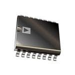
| 封装/外壳 | 16-SOIC(0.295",7.50mm 宽) |
| 封装/箱体 | SOIC-16 |
| 工作温度 | -40°C ~ 85°C |
| 工作电源电压 | 5 V |
| 工厂包装数量 | 47 |
| 接口类型 | Serial (3-Wire, SPI, QSPI, Microwire) |
| 数据接口 | DSP,MICROWIRE™,QSPI™,串行,SPI™ |
| 最大功率耗散 | 6.5 mW |
| 最大工作温度 | + 85 C |
| 最小工作温度 | - 40 C |
| 标准包装 | 47 |
| 特性 | PGA |
| 电压参考 | External |
| 电压源 | 单电源 |
| 系列 | AD7705 |
| 结构 | Sigma-Delta |
| 转换器数 | 1 |
| 转换器数量 | 1 |
| 转换速率 | 500 S/s |
| 输入数和类型 | 2 个差分,单极2 个差分,双极 |
| 输入类型 | Differential |
| 通道数量 | 2 Channel |
| 配用 | /product-detail/zh/EVAL-AD7705EBZ/EVAL-AD7705EBZ-ND/1551307 |
| 采样率(每秒) | 500 |


- 商务部:美国ITC正式对集成电路等产品启动337调查
- 曝三星4nm工艺存在良率问题 高通将骁龙8 Gen1或转产台积电
- 太阳诱电将投资9.5亿元在常州建新厂生产MLCC 预计2023年完工
- 英特尔发布欧洲新工厂建设计划 深化IDM 2.0 战略
- 台积电先进制程称霸业界 有大客户加持明年业绩稳了
- 达到5530亿美元!SIA预计今年全球半导体销售额将创下新高
- 英特尔拟将自动驾驶子公司Mobileye上市 估值或超500亿美元
- 三星加码芯片和SET,合并消费电子和移动部门,撤换高东真等 CEO
- 三星电子宣布重大人事变动 还合并消费电子和移动部门
- 海关总署:前11个月进口集成电路产品价值2.52万亿元 增长14.8%


PDF Datasheet 数据手册内容提取
3 V/5 V, 1 mW, 2-/3-Channel, 16-Bit, Sigma-Delta ADCs AD7705/AD7706 FEATURES FUNCTIONAL BLOCK DIAGRAM AD7705: 2 fully differential input channel ADCs VDD REF IN(–) REF IN(+) AD7706: 3 pseudo differential input channel ADCs AD7705/AD7706 16 bits no missing codes CHARGE 0.003% nonlinearity BALANCING A/D CONVERTER Programmable gain front end: gains from 1 to 128 ANALOG Σ -Δ 3-wire serial interface INPUT MAX BUFFER PGA MODULATOR CHANNELS SPI®-, QSPI™-, MICROWIRE™-, and DSP-compatible A = 1≈128 Schmitt-trigger input on SCLK DIGITAL FILTER Ability to buffer the analog input 2.7 V to 3.3 V or 4.75 V to 5.25 V operation Power dissipation 1 mW maximum @ 3 V Standby current 8 μA maximum SERIAL INTERFACE 16-lead PDIP, 16-lead SOIC, and 16-lead TSSOP packages REGISTER BANK MCLK IN CLOCK SCLK GENERAL DESCRIPTION MCLK OUT GENERATION CS DIN The AD7705/AD7706 are complete analog front ends for low DOUT frequency measurement applications. These 2-/3-channel devices cparnod aucccee pste rloiawl dleigvietla iln opuuttp suitg. nTahlse ddierveicctelys fermompl oay t raa Σn-sΔdu cer and GND DRDY RESET 01166-001 Figure 1. conversion technique to realize up to 16 bits of no missing codes performance. The selected input signal is applied to a The AD7705/AD7706 devices, with a 3 V supply and a 1.225 V proprietary, programmable-gain front end based around an reference, can handle unipolar input signal ranges of 0 mV to analog modulator. The modulator output is processed by an on- 10 mV through 0 V to 1.225 V. The devices can accept bipolar chip digital filter. The first notch of this digital filter can be pro- input ranges of ±10 mV through ±1.225 V. Therefore, the grammed via an on-chip control register, allowing adjustment of AD7705/AD7706 devices perform all signal conditioning and the filter cutoff and output update rate. conversion for a 2-channel or 3-channel system. The AD7705/AD7706 devices operate from a single 2.7 V to The AD7705/AD7706 are ideal for use in smart, microcontroller, 3.3 V or 4.75 V to 5.25 V supply. The AD7705 features two fully or DSP-based systems. The devices feature a serial interface that differential analog input channels; the AD7706 features three can be configured for 3-wire operation. Gain settings, signal pseudo differential input channels. polarity, and update rate selection can be configured in software using the input serial port. The parts contains self-calibration and Both devices feature a differential reference input. Input signal system calibration options to eliminate gain and offset errors on ranges of 0 mV to 20 mV through 0 V to 2.5 V can be the part itself or in the system. CMOS construction ensures very incorporated on both devices when operating with a V of 5 V DD low power dissipation, and the power-down mode reduces the and a reference of 2.5 V. They can also handle bipolar input standby power consumption to 20 μW typ. signal ranges of ±20 mV through ±2.5 V, which are referenced to the AIN(−) inputs on the AD7705 and to the COMMON input These parts are available in a 16-lead, wide body (0.3 inch), on the AD7706. plastic dual in-line package (DIP); a 16-lead, wide body (0.3 inch), standard small outline (SOIC) package; and a low profile, 16-lead, thin shrink small outline package (TSSOP). Rev. C Information furnished by Analog Devices is believed to be accurate and reliable. However, no responsibility is assumed by Analog Devices for its use, nor for any infringements of patents or other One Technology Way, P.O. Box 9106, Norwood, MA 02062-9106, U.S.A. rights of third parties that may result from its use. Specifications subject to change without notice. No license is granted by implication or otherwise under any patent or patent rights of Analog Devices. Tel: 781.329.4700 www.analog.com Trademarks and registered trademarks are the property of their respective owners. Fax: 781.461.3113 ©2006 Analog Devices, Inc. All rights reserved.
AD7705/AD7706 TABLE OF CONTENTS Features..............................................................................................1 Reference Input...........................................................................23 General Description.........................................................................1 Digital Filtering...........................................................................23 Functional Block Diagram..............................................................1 Analog Filtering..........................................................................25 Revision History...............................................................................3 Calibration...................................................................................25 Product Highlights...........................................................................4 Theory of Operation......................................................................28 Specifications.....................................................................................5 Clocking and Oscillator Circuit...............................................28 Timing Characteristics................................................................8 System Synchronization............................................................28 Absolute Maximum Ratings............................................................9 RESET Input...............................................................................29 ESD Caution..................................................................................9 Standby Mode.............................................................................29 Pin Configurations and Function Descriptions.........................10 Accuracy......................................................................................29 Output Noise (5 V Operation)......................................................12 Drift Considerations..................................................................29 Output Noise (3 V Operation)......................................................13 Power Supplies............................................................................30 Typical Performance Characteristics...........................................14 Supply Current............................................................................30 On-Chip Registers..........................................................................16 Grounding and Layout..............................................................30 Communication Register (RS2, RS1, RS0 = 0, 0, 0)...............16 Evaluating the Performance......................................................31 Setup Register (RS2, RS1, RS0 = 0, 0, 1); Power-On/Reset Digital Interface..........................................................................31 Status: 01 Hexadecimal..............................................................17 Configuring the AD7705/AD7706..........................................33 Clock Register (RS2, RS1, RS0 = 0, 1, 0); Power-On/Reset Status: 05 Hexadecimal..............................................................19 Microcomputer/Microprocessor Interfacing.........................34 Data Register (RS2, RS1, RS0 = 0, 1, 1)...................................20 Code For Setting Up the AD7705/AD7706............................35 Applications.....................................................................................38 Test Register (RS2, RS1, RS0 = 1, 0, 0); Power-On/Reset Status: 00 Hexadecimal..............................................................20 Pressure Measurement...............................................................38 Zero-Scale Calibration Register (RS2, RS1, RS0 = 1, 1, 0); Temperature Measurement.......................................................39 Power-On/Reset Status: 1F4000 Hexadecimal...........................20 Smart Transmitters.....................................................................40 Full-Scale Calibration Register (RS2, RS1, RS0 = 1, 1, 1); Power-On/Reset Status: 5761AB HexaDecimal.........................20 Battery Monitoring....................................................................41 Circuit Description.........................................................................21 Outline Dimensions.......................................................................42 Analog Input...............................................................................22 Ordering Guide..........................................................................43 Bipolar/Unipolar Input..............................................................22 Rev. C | Page 2 of 44
AD7705/AD7706 REVISION HISTORY 5/06—Rev. B to Rev. C Updated Format..................................................................Universal Changes to Table 1............................................................................3 Updated Outline Dimensions........................................................42 Changes to Ordering Guide...........................................................43 6/05—Rev. A to Rev. B Updated Format..................................................................Universal Changed Range of Absolute Voltage on Analog InputsUniversal Changes to Table 19........................................................................21 Updated Outline Dimensions........................................................42 Changes to Ordering Guide...........................................................43 11/98—Rev. 0 to Rev. A Revision 0: Initial Version Rev. C | Page 3 of 44
AD7705/AD7706 PRODUCT HIGHLIGHTS 1. The AD7705/AD7706 devices consume less than 1 mW at 3. The AD7705/AD7706 are ideal for microcontroller or DSP 3 V supplies and 1 MHz master clock, making them ideal processor applications with a 3-wire serial interface, for use in low power systems. Standby current is less than 8 reducing the number of interconnect lines and reducing μA. the number of opto-couplers required in isolated systems. 2. The programmable gain input allows the AD7705/AD7706 4. The parts feature excellent static performance to accept input signals directly from a strain gage or specifications with 16 bits, no missing codes, ±0.003% transducer, removing a considerable amount of signal accuracy, and low rms noise (<600 nV). Endpoint errors conditioning. and the effects of temperature drift are eliminated by on- chip calibration options, which remove zero-scale and full- scale errors. Rev. C | Page 4 of 44
AD7705/AD7706 SPECIFICATIONS V = 3 V or 5 V, REF IN(+) = 1.225 V with V = 3 V, and 2.5 V with V = 5 V; REF IN(−) = GND; MCLK IN = 2.4576 MHz, unless DD DD DD otherwise noted. All specifications T to T , unless otherwise noted. MIN MAX Table 1. Parameter B Version1 Unit Conditions/Comments STATIC PERFORMANCE No Missing Codes 16 Bits min Guaranteed by design, filter notch < 60 Hz Output Noise See Table 5 and Depends on filter cutoffs and selected gain Table 7 Integral Nonlinearity2 ±0.003 % of FSR max Filter notch < 60 Hz, typically ±0.0003% Unipolar Offset Error3 Unipolar Offset Drift4 0.5 μV/°C typ Bipolar Zero Error3 Bipolar Zero Drift4 0.5 μV/°C typ For gains 1, 2, and 4 0.1 μV/°C typ For gains 8, 16, 32, 64, and 128 Positive Full-Scale Error3, 5 Full-Scale Drift4, 6 0.5 μV/°C typ Gain Error3, 7 Gain Drift4, 8 0.5 ppm of FSR/°C typ Bipolar Negative Full-Scale Error2 ±0.003 % of FSR typ Typically ±0.001% Bipolar Negative Full-Scale Drift4 1 μV/°C typ For gains of 1 to 4 0.6 μV/°C typ For gains of 8 to 128 ANALOG INPUTS/REFERENCE INPUTS Specifications for AIN and REF IN, unless otherwise noted Common-Mode Rejection (CMR)2 V = 5 V DD Gain = 1 96 dB typ Gain = 2 105 dB typ Gain = 4 110 dB typ Gain = 8 to 128 130 dB typ V = 3 V DD Gain = 1 105 dB typ Gain = 2 110 dB typ Gain = 4 120 dB typ Gain = 8 to 128 130 dB typ Normal-Mode 50 Hz Rejection2 98 dB typ For filter notches of 25 Hz, 50 Hz, ±0.02 × f NOTCH Normal-Mode 60 Hz Rejection2 98 dB typ For filter notches of 20 Hz, 60 Hz, ±0.02 × f NOTCH Common-Mode 50 Hz Rejection2 150 dB typ For filter notches of 25 Hz, 50 Hz, ±0.02 × f NOTCH Common-Mode 60 Hz Rejection2 150 dB typ For filter notches of 20 Hz, 60 Hz, ±0.02 × f NOTCH Absolute/Common-Mode REF IN GND to V V min to V max DD Voltage2 Absolute/Common-Mode AIN GND − 100 mV V min BUF bit of setup register = 0 Voltage2, 9, 10 V + 30 mV V max DD Absolute/Common-Mode AIN GND + 50 mV V min BUF bit of setup register = 1 Voltage2, 9 V − 1.5 V V max DD AIN DC Input Current2 1 nA max AIN Sampling Capacitance2 10 pF max AIN Differential Voltage Range11 0 to +V /gain12 nom Unipolar input range (B/U bit of setup register = 1) REF ±V /gain nom Bipolar input range (B/U bit of setup register = 0) REF Rev. C | Page 5 of 44
AD7705/AD7706 Parameter B Version1 Unit Conditions/Comments AIN Input Sampling Rate, f Gain × f /64 For gains of 1 to 4 S CLKIN f /8 For gains of 8 to 128 CLKIN Reference Input Range REF IN(+) − REF IN(−) Voltage 1/1.75 V min/V max V = 2.7 V to 3.3 V DD V = 1.225 ± 1% for specified performance REF REF IN(+) − REF IN(−) Voltage 1/3.5 V min/V max V = 4.75 V to 5.25 V DD V = 2.5 ± 1% for specified performance REF REF IN Input Sampling Rate, f f /64 S CLKIN LOGIC INPUTS Input Current All Inputs, Except MCLK IN ±1 μA max Typically ±20 nA MCLK IN ±10 μA max Typically ±2 μA All Inputs, Except SCLK and MCLK IN Input Low Voltage, V 0.8 V max V = 5 V INL DD 0.4 V max V = 3 V DD Input High Voltage, V 2.0 V min V = 3 V and 5 V INH DD SCLK Only (Schmitt-Triggered Input) V = 5 V nominal DD V 1.4/3 V min/V max T+ V 0.8/1.4 V min/V max T− V − V 0.4/0.8 V min/V max T+ T− SCLK Only (Schmitt-Triggered Input) V = 3 V nominal DD V 1/2 V min/V max T+ V 0.4/1.1 V min/V max T− V − V 0.375/0.8 V min/V max T+ T− MCLK IN Only V = 5 V nominal DD Input Low Voltage, V 0.8 V max INL Input High Voltage, V 3.5 V min INH MCLK IN Only V = 3 V nominal DD Input Low Voltage, V 0.4 V max INL Input High Voltage, V 2.5 V min INH LOGIC OUTPUTS (Including MCLK OUT) Output Low Voltage, V 0.4 V max I = 800 μA, except for MCLK OUT;13 V = 5 V OL SINK DD Output Low Voltage, V 0.4 V max I = 100 μA, except for MCLK OUT;13 V = 3 V OL SINK DD Output High Voltage, V 4 V min I = 200 μA, except for MCLK OUT;13 V = 5 V OH SOURCE DD Output High Voltage, V V − 0.6 V min I = 100 μA, except for MCLK OUT;13 V = 3 V OH DD SOURCE DD Floating State Leakage Current ±10 μA max Floating State Output Capacitance14 9 pF typ Data Output Coding Binary Unipolar mode Offset binary Bipolar mode SYSTEM CALIBRATION Positive Full-Scale Limit15 (1.05 × V )/gain V max Gain is the selected PGA gain (1 to 128) REF Negative Full-Scale Limit15 −(1.05 × V )/gain V max Gain is the selected PGA gain (1 to 128) REF Offset Limit15 −(1.05 × V )/gain V max Gain is the selected PGA gain (1 to 128) REF Input Span16 (0.8 × V )/gain V min Gain is the selected PGA gain (1 to 128) REF (2.1 × V )/gain V max Gain is the selected PGA gain (1 to 128) REF Rev. C | Page 6 of 44
AD7705/AD7706 Parameter B Version1 Unit Conditions/Comments POWER REQUIREMENTS V Voltage 2.7 to 3.3 V min to V max For specified performance DD Power Supply Currents17 Digital I/Ps = 0 V or V , external MCLK IN and CLKDIS = 1 DD 0.32 mA max BUF bit = 0, f = 1 MHz, gains of 1 to 128 CLKIN 0.6 mA max BUF bit = 1, f = 1 MHz, gains of 1 to 128 CLKIN 0.4 mA max BUF bit = 0, f = 2.4576 MHz, gains of 1 to 4 CLKIN 0.6 mA max BUF bit = 0, f = 2.4576 MHz, gains of 8 to 128 CLKIN 0.7 mA max BUF bit = 1, f = 2.4576 MHz, gains of 1 to 4 CLKIN 1.1 mA max BUF bit = 1, f = 2.4576 MHz, gains of 8 to 128 CLKIN V Voltage 4.75 to 5.25 V min to V max For specified performance DD Power Supply Currents17 Digital I/Ps = 0 V or V , external MCLK IN and CLKDIS = 1 DD 0.45 mA max BUF bit = 0, f = 1 MHz, gains of 1 to 128 CLKIN 0.7 mA max BUF bit = 1, f = 1 MHz, gains of 1 to 128 CLKIN 0.6 mA max BUF bit = 0, f = 2.4576 MHz, gains of 1 to 4 CLKIN 0.85 mA max BUF bit = 0, f = 2.4576 MHz, gains of 8 to 128 CLKIN 0.9 mA max BUF bit = 1, f = 2.4576 MHz, gains of 1 to 4 CLKIN 1.3 mA max BUF bit = 1, f = 2.4576 MHz, gains of 8 to 128 CLKIN Standby (Power-Down) Current18 16 μA max External MCLK IN = 0 V or V , V = 5 V, see Figure 12 DD DD 8 μA max External MCLK IN = 0 V or V , V = 3 V DD DD Power Supply Rejection19, 20 dB typ 1 Temperature range is −40°C to +85°C. 2 These numbers are established from characterization or design data at initial product release. 3 A calibration is effectively a conversion; therefore, these errors are of the order of the conversion noise shown in Table 5 and Table 7. This applies after calibration at the temperature of interest. 4 Recalibration at any temperature removes these drift errors. 5 Positive full-scale error includes zero-scale errors (unipolar offset error or bipolar zero error) and applies to both unipolar and bipolar input ranges. 6 Full-scale drift includes zero-scale drift (unipolar offset drift or bipolar zero drift) and applies to both unipolar and bipolar input ranges. 7 Gain error does not include zero-scale errors. It is calculated as (full-scale error – unipolar offset error) for unipolar ranges and (full-scale error - bipolar zero error) for bipolar ranges. 8 Gain drift does not include unipolar offset drift or bipolar zero drift. It is effectively the drift of the part if only zero-scale calibrations are performed. 9 This common-mode voltage range is allowed, provided that the input voltage on analog inputs is not more positive than VDD + 30 mV or more negative than GND − 100 mV. Parts are functional with voltages down to GND − 200 mV, but with increased leakage at high temperatures. 10 The AD7705/AD7706 can tolerate absolute analog input voltages down to GND − 200 mV, but the leakage current increases. 11 The analog input voltage range on AIN(+) is given with respect to the voltage on AIN(−) on the AD7705, and with respect to the voltage of the COMMON input on the AD7706. The absolute voltage on the analog inputs should not be more positive than VDD + 30 mV, or more negative than GND − 100 mV for specified performance. Input voltages of GND − 200 mV can be accommodated, but with increased leakage at high temperatures. 12 VREF = REFIN(+) − REFIN(−). 13 These logic output levels apply to the MCLK OUT only when it is loaded with one CMOS load. 14 Sample tested at 25°C to ensure compliance. 15 After calibration, if the analog input exceeds positive full scale, the converter outputs all 1s. If the analog input is less than negative full scale, the device outputs all 0s. 16 These calibration and span limits apply, provided that the absolute voltage on the analog inputs does not exceed VDD + 30 mV or go more negative than GND − 100 mV. The offset calibration limit applies to both the unipolar zero point and the bipolar zero point. 17 When using a crystal or ceramic resonator across the MCLK pins as the clock source for the device, the VDD current and power dissipation varies depending on the crystal or resonator type (see Clocking and Oscillator Circuit section). 18 If the external master clock continues to run in standby mode, the standby current increases to 150 μA typical at 5 V and 75 μA at 3 V. When using a crystal or ceramic resonator across the MCLK pins as the clock source for the device, the internal oscillator continues to run in standby mode, and the power dissipation depends on the crystal or resonator type (see Standby Mode section). 19 Measured at dc and applies in the selected pass band. PSRR at 50 Hz exceeds 120 dB, with filter notches of 25 Hz or 50 Hz. PSRR at 60 Hz exceeds 120 dB, with filter notches of 20 Hz or 60 Hz. 20 PSRR depends on both gain and VDD, as follows: Gain 1 2 4 8 to 128 VDD = 3 V 86 78 85 93 VDD = 5 V 90 78 84 91 Rev. C | Page 7 of 44
AD7705/AD7706 TIMING CHARACTERISTICS V = 2.7 V to 5.25 V; GND = 0 V; f = 2.4576 MHz; Input Logic 0 = 0 V, Logic 1 = V , unless otherwise noted. DD CLKIN DD Table 2. Timing Characteristics1, 2 Limit at T , T MIN MAX Parameter (B Version) Unit Conditions/Comments f 3, 4 400 kHz min Master clock frequency (crystal oscillator or externally supplied) CLKIN 2.5 MHz max For specified performance t 0.4 × t ns min Master clock input low time, t = 1/f CLKIN LO CLKIN CLKIN CLKIN t 0.4 × t ns min Master clock input high time CLKIN HI CLKIN t 500 × t ns nom DRDY high time 1 CLKIN t 100 ns min RESET pulse width 2 Read Operation t 0 ns min DRDY to CS setup time 3 t 120 ns min CS falling edge to SCLK rising edge setup time 4 t 5 0 ns min SCLK falling edge to data valid delay 5 80 ns max V = 5 V DD 100 ns max V = 3.0 V DD t 100 ns min SCLK high pulse width 6 t 100 ns min SCLK low pulse width 7 t 0 ns min CS rising edge to SCLK rising edge hold time 8 t 6 10 ns min Bus relinquish time after SCLK rising edge 9 60 ns max V = 5 V DD 100 ns max V = 3.0 V DD t 100 ns max SCLK falling edge to DRDY high7 10 Write Operation t 120 ns min CS falling edge to SCLK rising edge setup time 11 t 30 ns min Data valid to SCLK rising edge setup time 12 t 20 ns min Data valid to SCLK rising edge hold time 13 t 100 ns min SCLK high pulse width 14 t 100 ns min SCLK low pulse width 15 t 0 ns min CS rising edge to SCLK rising edge hold time 16 1 Sample tested at 25°C to ensure compliance. All input signals are specified with tR = tF = 5 ns (10% to 90% of VDD) and timed from a voltage level of 1.6 V. 2 See Figure 19 and Figure 20. 3 The fCLKIN duty cycle range is 45% to 55%. fCLKIN must be supplied whenever the AD7705/AD7706 are not in standby mode. If no clock is present, the devices can draw higher current than specified, and possibly become uncalibrated. 4 The AD7705/AD7706 are production tested with fCLKIN at 2.4576 MHz (1 MHz for some IDD tests). They are guaranteed by characterization to operate at 400 kHz. 5 These numbers are measured with the load circuit of Figure 2 and defined as the time required for the output to cross the VOL or VOH limits. 6 These numbers are derived from the measured time taken by the data output to change 0.5 V when loaded with the circuit of Figure 2. The measured number is then extrapolated back to remove effects of charging or discharging the 50 pF capacitor. This means that the times quoted in the timing characteristics are the true bus relinquish times of the part and as such are independent of external bus loading capacitances. 7 DRDY returns high upon completion of the first read from the device after an output update. The same data can be reread while DRDY is high, but care should be taken that subsequent reads do not occur close to the next output update. ISINK (800μA AT VDD = 5V 100μA AT VDD = 3V) TO OUTPUT 1.6V PIN 50pF ISOURCE1 (0200m0μAA A ATT V VDDDD = = 3 5VV) 01166-002 Figure 2. Load Circuit for Access Time and Bus Relinquish Time Rev. C | Page 8 of 44
AD7705/AD7706 ABSOLUTE MAXIMUM RATINGS T = 25°C, unless otherwise noted. A Table 3. Stresses above those listed under Absolute Maximum Ratings Parameters Ratings may cause permanent damage to the device. This is a stress VDD to GND −0.3 V to +7 V rating only; functional operation of the device at these or any Analog Input Voltage to GND −0.3 V to VDD + 0.3 V other conditions above those indicated in the operational Reference Input Voltage to GND −0.3 V to VDD + 0.3 V section of this specification is not implied. Exposure to absolute Digital Input Voltage to GND −0.3 V to VDD + 0.3 V maximum rating conditions for extended periods may affect Digital Output Voltage to GND −0.3 V to VDD + 0.3 V device reliability. Operating Temperature Range Commercial (B Version) −40°C to + 85°C Storage Temperature Range −65°C to + 150°C Junction Temperature 150°C PDIP Package, Power Dissipation 450 mW θ Thermal Impedance 105°C/W JA Lead Temperature (Soldering, 10 sec) 260°C SOIC Package, Power Dissipation 450 mW θ Thermal Impedance 75°C/W JA Lead Temperature, Soldering Vapor Phase (60 sec) 215°C Infrared (15 sec) 220°C SSOP Package, Power Dissipation 450 mW θ Thermal Impedance 139°C/W JA Lead Temperature, Soldering Vapor Phase (60 sec) 215°C Infrared (15 sec) 220°C ESD Rating >4000 V ESD CAUTION ESD (electrostatic discharge) sensitive device. Electrostatic charges as high as 4000 V readily accumulate on the human body and test equipment and can discharge without detection. Although this product features proprietary ESD protection circuitry, permanent damage may occur on devices subjected to high energy electrostatic discharges. Therefore, proper ESD precautions are recommended to avoid performance degradation or loss of functionality. Rev. C | Page 9 of 44
AD7705/AD7706 PIN CONFIGURATIONS AND FUNCTION DESCRIPTIONS SCLK 1 16 GND SCLK 1 16 GND MCLK IN 2 15 VDD MCLK IN 2 15 VDD MCLK OUT 3 AD7705 14 DIN MCLK OUT 3 AD7706 14 DIN CS 4 TOP VIEW 13 DOUT CS 4 (NToOt Pto V SIEcaWle) 13 DOUT RESET 5 (Not to Scale) 12 DRDY RESET 5 12 DRDY AIN2(+) 6 11 AIN2(–) AIN1 6 11 AIN3 AAIINN11((+–)) 78 190 RREEFF IINN((+–)) 01166-003 COMMAIONN2 78 190 RREEFF IINN((+–)) 01166-004 Figure 3. AD7705 Pin Configuration Figure 4. AD7706 Pin Configuration Table 4. Pin Function Descriptions Mnemonic Pin No. AD7705 AD7706 Description 1 SCLK SCLK Serial Clock. An external serial clock is applied to the Schmitt-triggered logic input to access serial data from the AD7705/AD7706. This serial clock can be a continuous clock with all data transmitted in a continuous train of pulses. Alternatively, it can be a noncontinuous clock with the information transmitted to the AD7705/AD7706 in smaller batches of data. 2 MCLK IN MCLK IN Master Clock Signal. This can be provided in the form of a crystal/resonator or external clock. A crystal/resonator can be tied across the Pin MCLK IN and Pin MCLK OUT. Alternatively, the MCLK IN pin can be driven with a CMOS-compatible clock with the MCLK OUT pin left unconnected. The parts can be operated with clock frequencies in the range of 500 kHz to 5 MHz. 3 MCLK OUT MCLK OUT When the master clock for these devices is a crystal/resonator, the crystal/resonator is connected between Pin MCLK IN and Pin MCLK OUT. If an external clock is applied to Pin MCLK IN, Pin MCLK OUT provides an inverted clock signal. This clock can be used to provide a clock source for external circuitry and is capable of driving 1 CMOS load. If the user does not require this clock externally, Pin MCLK OUT can be turned off via the CLKDIS bit of the clock register. This ensures that the part does not unnecessarily burn power driving capacitive loads on Pin MCLK OUT. 4 CS CS Chip Select. Active low logic input used to select the AD7705/AD7706. With this input hardwired low, the AD7705/AD7706 can operate in its 3-wire interface mode with Pin SCLK, Pin DIN, and Pin DOUT used to interface to the device. The CS pin can be used to select the device communicating with the AD7705/AD7706. 5 RESET RESET Logic Input. Active low input that resets the control logic, interface logic, calibration coefficients, digital filter, and analog modulator of the parts to power-on status. 6 AIN2(+) AIN1 Positive Input of the Differential Analog Input Pair AIN2(+)/AIN2(−) for AD7705. Channel 1 for AD7706. 7 AIN1(+) AIN2 Positive Input of the Differential Analog Input Pair AIN1(+)/AIN1(−) for AD7705. Channel 2 for AD7706. 8 AIN1(−) COMMON Negative Input of the Differential Analog Input Pair AIN1(+)/AIN1(−) for AD7705. COMMON input for AD7706 with Channel 1, Channel 2, and Channel 3 referenced to this input. 9 REF IN(+) REF IN(+) Reference Input. Positive input of the differential reference input to the AD7705/AD7706. The reference input is differential with the provision that REF IN(+) must be greater than REF IN(−). REF IN(+) can lie anywhere between V and GND. DD 10 REF IN(−) REF IN(−) Reference Input. Negative input of the differential reference input to the AD7705/AD7706. The REF IN(−) can lie anywhere between V and GND, provided that REF IN(+) is greater than REF IN(−). DD 11 AIN2(−) AIN3 Negative Input of the Differential Analog Input Pair AIN2(+)/AIN2(−) for AD7705. Channel 3 for AD7706. 12 DRDY DRDY Logic Output. A logic low on this output indicates that a new output word is available from the AD7705/AD7706 data register. The DRDY pin returns high upon completion of a read operation of a full output word. If no data read has taken place between output updates, the DRDY line returns high for 500 × t cycles prior to the next output update. While DRDY is high, a read operation should CLK IN neither be attempted nor in progress to avoid reading from the data register as it is being updated. The DRDY line returns low after the update has taken place. DRDY is also used to indicate when the AD7705/AD7706 has completed its on-chip calibration sequence. 13 DOUT DOUT Serial Data Output. Serial data is read from the output shift register on the part. The output shift register can contain information from the setup register, communication register, clock register, or data register, depending on the register selection bits of the communication register. Rev. C | Page 10 of 44
AD7705/AD7706 Mnemonic Pin No. AD7705 AD7706 Description 14 DIN DIN Serial Data Input. Serial data is written to the input shift register on the part. Data from the input shift register is transferred to the setup register, clock register, or communication register, depending on the register selection bits of the communication register. 15 V V Supply Voltage. 2.7 V to 5.25 V operation. DD DD 16 GND GND Ground Reference Point for the AD7705/AD7706 Internal Circuitry. Rev. C | Page 11 of 44
AD7705/AD7706 OUTPUT NOISE (5 V OPERATION) Table 5 shows the AD7705/AD7706 output rms noise for the Note that these numbers represent the resolution for which selectable notch and −3 dB frequencies for the parts, as selected there is no code flicker. They are not calculated based on rms by FS0 and FS1 of the clock register. The numbers given are for noise, but on peak-to-peak noise. The numbers given are for the bipolar input ranges with a V of 2.5 V and V = 5 V. bipolar input ranges with a V of 2.5 V for either buffered or REF DD REF These numbers are typical and are generated at an analog input unbuffered mode. These numbers are typical and are rounded voltage of 0 V with the parts used in either buffered or unbuffered to the nearest LSB. The numbers apply for the CLKDIV bit of mode. Table 6 shows the output peak-to-peak noise for the the clock register set to 0. selectable notch and −3 dB frequencies for the parts. Table 5. Output RMS Noise vs. Gain and Output Update Rate @ 5 V Filter First Typical Output RMS Noise in μV Notch and −3 dB O/P Data Rate Frequency Gain of 1 Gain of 2 Gain of 4 Gain of 8 Gain of 16 Gain of 32 Gain of 64 Gain of 128 MCLK IN = 2.4576 MHz 50 Hz 13.1 Hz 4.1 2.1 1.2 0.75 0.7 0.66 0.63 0.6 60 Hz 15.72 Hz 5.1 2.5 1.4 0.8 0.75 0.7 0.67 0.62 250 Hz 65.5 Hz 110 49 31 17 8 3.6 2.3 1.7 500 Hz 131 Hz 550 285 145 70 41 22 9.1 4.7 MCLK IN = 1 MHz 20 Hz 5.24 Hz 4.1 2.1 1.2 0.75 0.7 0.66 0.63 0.6 25 Hz 6.55 Hz 5.1 2.5 1.4 0.8 0.75 0.7 0.67 0.62 100 Hz 26.2 Hz 110 49 31 17 8 3.6 2.3 1.7 200 Hz 52.4 Hz 550 285 145 70 41 22 9.1 4.7 Table 6. Peak-to-Peak Resolution vs. Gain and Output Update Rate @ 5 V Filter First Typical Peak-to-Peak Resolution Bits Notch and −3 dB O/P Data Rate Frequency Gain of 1 Gain of 2 Gain of 4 Gain of 8 Gain of 16 Gain of 32 Gain of 64 Gain of 128 MCLK IN = 2.4576 MHz 50 Hz 13.1 Hz 16 16 16 16 16 16 15 14 60 Hz 15.72 Hz 16 16 16 16 15 14 14 13 250 Hz 65.5 Hz 13 13 13 13 13 13 12 12 500 Hz 131 Hz 10 10 10 10 10 10 10 10 MCLK IN = 1 MHz 20 Hz 5.24 Hz 16 16 16 16 16 16 15 14 25 Hz 6.55 Hz 16 16 16 16 15 14 14 13 100 Hz 26.2 Hz 13 13 13 13 13 13 12 12 200 Hz 52.4 Hz 10 10 10 10 10 10 10 10 Rev. C | Page 12 of 44
AD7705/AD7706 OUTPUT NOISE (3 V OPERATION) Table 7 shows the AD7705/AD7706 output rms noise for the Note that these numbers represent the resolution for which selectable notch and −3 dB frequencies for the parts, as selected there is no code flicker. They are not calculated based on rms by FS0 and FS1 of the clock register. The numbers given are for noise, but on peak-to-peak noise. The numbers given are for the bipolar input ranges with a V of 1.225 V and a V = 3 V. bipolar input ranges with a V of 1.225 V for either buffered or REF DD REF These numbers are typical and are generated at an analog input unbuffered mode. These numbers are typical and are rounded voltage of 0 V with the parts used in either buffered or unbuffered to the nearest LSB. The numbers apply for the CLKDIV bit of mode. Table 8 shows the output peak-to-peak noise for the the clock register set to 0. selectable notch and −3 dB frequencies for the parts. Table 7. Output RMS Noise vs. Gain and Output Update Rate @ 3 V Filter First Typical Output RMS Noise in μV Notch and −3 dB O/P Data Rate Frequency Gain of 1 Gain of 2 Gain of 4 Gain of 8 Gain of 16 Gain of 32 Gain of 64 Gain of 128 MCLK IN = 2.4576 MHz 50 Hz 13.1 Hz 3.8 2.4 1.5 1.3 1.1 1.0 0.9 0.9 60 Hz 15.72 Hz 5.1 2.9 1.7 1.5 1.2 1.0 0.9 0.9 250 Hz 65.5 Hz 50 25 14 9.9 5.1 2.6 2.3 2.0 500 Hz 131 Hz 270 135 65 41 22 9.7 5.1 3.3 MCLK IN = 1 MHz 20 Hz 5.24 Hz 3.8 2.4 1.5 1.3 1.1 1.0 0.9 0.9 25 Hz 6.55 Hz 5.1 2.9 1.7 1.5 1.2 1.0 0.9 0.9 100 Hz 26.2 Hz 50 25 14 9.9 5.1 2.6 2.3 2.0 200 Hz 52.4 Hz 270 135 65 41 22 9.7 5.1 3.3 Table 8. Peak-to-Peak Resolution vs. Gain and Output Update Rate @ 3 V Filter First Typical Peak-to-Peak Resolution in Bits Notch and −3 dB O/P Data Rate Frequency Gain of 1 Gain of 2 Gain of 4 Gain of 8 Gain of 16 Gain of 32 Gain of 64 Gain of 128 MCLK IN = 2.4576 MHz 50 Hz 13.1 Hz 16 16 15 15 14 13 13 12 60 Hz 15.72 Hz 16 16 15 14 14 13 13 12 250 Hz 65.5 Hz 13 13 13 13 12 12 11 11 500 Hz 131 Hz 10 10 10 10 10 10 10 10 MCLK IN = 1 MHz 20 Hz 5.24 Hz 16 16 15 15 14 13 13 12 25 Hz 6.55 Hz 16 16 15 14 14 13 13 12 100 Hz 26.2 Hz 13 13 13 13 12 12 11 11 200 Hz 52.4 Hz 10 10 10 10 10 10 10 10 Rev. C | Page 13 of 44
AD7705/AD7706 TYPICAL PERFORMANCE CHARACTERISTICS 32771 400 VDD = 5V TA = 25°C 32770 VGRAEINF == 2+.152V8 RMS NOISE = 600nV 50Hz UPDATE RATE 32769 300 E READ3322776678 RRENCE 200 D U O C C32766 OC 32765 100 3322776634 01166-005 0 01166-008 0 100 200 300 400 500 600 700 800 900 1000 32764 32765 32766 32767 32768 32769 32770 READING NUMBER CODE Figure 5. Noise @ Gain = +128 With 50 Hz Update Rate Figure 8. Histogram of Data in Figure 5 1.2 1.2 VDD = 3V VDD = 5V TA = 25°C BUFFERED MODE, GAIN = +128 TA = +25°C 1.0 1.0 BUFFERED MODE, GAIN = +128 0.8 0.8 BUFFERED MODE, GAIN = +1 A) BUFFERED MODE, GAIN = +1 A) (mD 0.6 (mD 0.6 D D I I 0.4 0.4 UNBUFFERED MODE, GAIN = +128 0.2 UNBUFFERED MODE, GAIN = +128 0.2 0 UNBUFFERED MODE, GAIN = +1 01166-006 0 UNBUFFERED MODE, GAIN = +1 01166-009 0.4 0.6 0.8 1.0 1.2 1.4 1.6 1.8 2.0 2.2 2.4 2.6 0.4 0.6 0.8 1.0 1.2 1.4 1.6 1.8 2.0 2.2 2.4 2.6 FREQUENCY (MHz) FREQUENCY (MHz) Figure 6. IDD vs. MCLK IN Frequency @ 3 V Figure 9. IDD vs. MCLK IN Frequency @ 5 V 1.0 1.2 BUFFERED MODE BUFFERED MODE 0.9 fCLK = 5MHz, fCLK = 5MHz, CLKDIV = 1 CLKDIV = 1 1.0 0.8 UNBUFFERED MODE BUFFERED MODE UNBUFFERED MODE BUFFERED MODE 0.7 fCCLLKK D=I V1 M=H 0z, fCLK U= N2B.4U5F76FMERHEz,D C MLKODDIEV = 0 0.8 fCCLLKK D=I V1 M=H 0z, fCLK =U N2.B45U7F6FMEHRzE, DC LMKODDIVE = 0 A) 0.6 fCLK = 5MHz, CLKDIV = 1 A) fCLK = 5MHz, CLKDIV = 1 m (D 0.5 (mD 0.6 D D I 0.4 UNBUFFERED MODE I UNBUFFERED MODE 0.3 fCLK = 2.84MHz, CLKDIV = 0 0.4 fCLK = 2.4576MHz, CLKDIV = 0 0.2 VDD = 3V VDD = 5V EXTERNAL MCLK BUFFERED MODE 0.2 EXTERNAL MCLK BUFFERED MODE 0.10 CTAL K=D 2I5S° C= 1 fCLK = 1MHz, CLKDIV = 0 01166-007 0 CTAL K=D 2I5S° C= 1 fCLK = 1MHz, CLKDIV = 0 01166-010 1 2 4 8 16 32 64 128 1 2 4 8 16 32 64 128 GAIN GAIN Figure 7. IDD vs. Gain and Clock Frequency @ 3 V Figure 10. IDD vs. Gain and Clock Frequency @ 5 V Rev. C | Page 14 of 44
AD7705/AD7706 20 TEK STOP: SINGLE SEQ 50.0kS/s VDD 16 1 A) MCLK IN = 0V OR VDD μ T ( EN 12 R R 2 U OSCILLATOR = 4.9152MHz Y C VDD = 5V B 8 D N A ST VDD = 3V 4 2 OSCILLATOR = 2.4576MHz 01166-011 0 01166-012 CH1 5.00V CH2 2.00V 5ms/DIV –40 –30 –20 –10 0 10 20 30 40 50 60 70 80 TEMPERATURE (°C) Figure 11. Crystal Oscillator Power-Up Time Figure 12. Standby Current vs. Temperature Rev. C | Page 15 of 44
AD7705/AD7706 ON-CHIP REGISTERS The second register is a setup register that determines calibration mode, gain setting, bipolar/unipolar operation, and The AD7705/AD7706 each contain eight on-chip registers that buffered mode. The third register is labeled the clock register can be accessed via the serial port. The first of these is a and contains the filter selection bits and clock control bits. The communication register that controls the channel selection, fourth register is the data register from which the output data is decides whether the next operation is a read or write operation, accessed. The final registers are the calibration registers, which and decides which register the next read or write operation store channel calibration data. The registers are discussed in accesses. more detail in the following sections. All communication to the AD7705/AD7706 must start with a COMMUNICATION REGISTER write operation to the communication register. After a power- (RS2, RS1, RS0 = 0, 0, 0) on or reset, the device expects a write to its communication register. The data written to this register determines whether The communication register is an 8-bit register from which data the next operation is a read or write operation and to which can be read or to which data can be written. All communication register this operation occurs. Therefore, write access to any to the part must start with a write operation to its communica- register on the part starts with a write operation to the tion register. The data written to the communication register communication register, followed by a write to the selected determines whether the next operation is a read or write register. Likewise, a read operation from any register on the operation and to which register this operation takes place. After part, including the communication register itself and the output the read or write operation is complete, the interface returns to data register, starts with a write operation to the communica- its default state, where it expects a write operation to the tion register, followed by a read operation from the selected communication register. In situations where the interface register. The communication register also controls the standby sequence is lost, a write operation of a least 32 serial clock mode and channel selection. The DRDY status is available by cycles with DIN high returns the ADC to its default state by reading from the communication register. resetting the part. Table 10 outlines the bit designations for the communication register. Table 9. Communication Register 0/DRDY (0) RS2 (0) RS1 (0) RS0 (0) R/W (0) STBY (0) CH1 (0) CH0 (0) Table 10. Communication Register Bit Description Register Description 0/DRDY For a write operation to the communications register, a 0 must be written to this bit. If a 1 is written to this bit, the part does not clock subsequent bits into the register. It stays at this bit location until a 0 is written. Then, the next seven bits are loaded into the communication register. For a read operation, this bit provides the status of the DRDY flag, which is the same as the DRDY output pin. RS2–RS0 Register Selection Bits. These bits are used to select which of the AD7705/AD7706 registers are being accessed during the serial interface communication. R/W Read/WRITE Select. This bit selects whether the next operation is a read or write operation. A 0 indicates a write cycle for the next operation to the selected register, and a 1 indicates a read operation from the selected register. STBY Standby. Writing 1 to this bit puts the part into standby or power-down mode. In this mode, the part consumes only 10 μA of power supply current. The part retains its calibration coefficients and control word information when in standby. Writing 0 to this bit places the parts in normal operating mode. CH1, CH0 Channel Select. These two bits select a channel for conversion or for access to the calibration coefficients, as outlined in Table 12. Following a calibration on a channel, three pairs of calibration registers store the calibration coefficients. Table 12 (for the AD7705) and Table 13 (for the AD7706) show which channel combinations have independent calibration coefficients. With CH1 at Logic 1 and CH0 at Logic 0, the AD7705 looks at the AIN1(−) input internally shorted to itself, while the AD7706 looks at the COMMON input internally shorted to itself. This can be used as a test method to evaluate the noise performance of the parts with no external noise sources. In this mode, the AIN1(−)/COMMON input should be connected to an external voltage within the allowable common-mode range for the parts. Rev. C | Page 16 of 44
AD7705/AD7706 Table 11. Register Selection RS2 RS1 RS0 Register Register Size 0 0 0 Communication register 8 bits 0 0 1 Setup register 8 bits 0 1 0 Clock register 8 bits 0 1 1 Data register 16 bits 1 0 0 Test register 8 bits 1 0 1 No operation 1 1 0 Offset register 24 bits 1 1 1 Gain register 24 bits Table 12. Channel Selection for AD7705 CH1 CH0 AIN(+) AIN(−) Calibration Register Pair 0 0 AIN1(+) AIN1(−) Register Pair 0 0 1 AIN2(+) AIN2(−) Register Pair 1 1 0 AIN1(−) AIN1(−) Register Pair 0 1 1 AIN1(−) AIN2(−) Register Pair 2 Table 13. Channel Selection for AD7706 CH1 CH0 AIN Reference Calibration Register Pair 0 0 AIN1 COMMON Register Pair 0 0 1 AIN2 COMMON Register Pair 1 1 0 COMMON COMMON Register Pair 0 1 1 AIN3 COMMON Register Pair 2 SETUP REGISTER (RS2, RS1, RS0 = 0, 0, 1); POWER-ON/RESET STATUS: 01 HEXADECIMAL The setup register is an 8-bit register from which data can be read or to which data can be written. Table 14 outlines the bit designations for the setup register. Table 14. Setup Register MD1 (0) MD0 (0) G2 (0) G1 (0) G0 (0) B/U (0) BUF (0) FSYNC (1) Table 15. Setup Register Description Register Description MD1, MD0 ADC Mode Bits. These bits select the operational mode of the ADC as outlined in Table 16. G2 to G0 Gain Selection Bits. These bits select the gain setting for the on-chip PGA, as outlined in Table 17. B/U Bipolar/Unipolar Operation. A 0 in this bit selects bipolar operation; a 1 in this bit selects unipolar operation. BUF Buffer Control. With this bit at 0, the on-chip buffer on the analog input is shorted out. With the buffer shorted out, the current flowing in the V line is reduced. When this bit is high, the on-chip buffer is in series with the analog input, allowing the input DD to handle higher source impedances. FSYNC Filter Synchronization. When this bit is high, the nodes of the digital filter, the filter control logic, the calibration control logic, and the analog modulator are held in a reset state. When this bit goes low, the modulator and filter start to process data, and a valid word is available in 3 × 1/output rate, that is, the settling time of the filter. This FSYNC bit does not affect the digital interface and does not reset the DRDY output if it is low. Rev. C | Page 17 of 44
AD7705/AD7706 Table 16. Operating Mode Options MD1 MD0 Operating Mode 0 0 Normal Mode. In this mode, the device performs normal conversions. 0 1 Self-Calibration. This activates self-calibration on the channel selected by CH1 and CH0 of the communication register. This is a one-step calibration sequence. When the sequence is complete, the part returns to normal mode, with both MD1 and MD0 returning to 0. The DRDY output or bit goes high when calibration is initiated, and returns low when self-calibration is complete and a new valid word is available in the data register. The zero-scale calibration is performed at the selected gain on internally shorted (zeroed) inputs, and the full-scale calibration is performed at the selected gain on an internally generated V /selected gain. REF 1 0 Zero-Scale System Calibration. This activates zero-scale system calibration on the channel selected by CH1 and CH0 of the communication register. Calibration is performed at the selected gain on the input voltage provided at the analog input during this calibration sequence. This input voltage should remain stable for the duration of the calibration. The DRDY output or bit goes high when calibration is initiated, and returns low when zero-scale calibration is complete and a new valid word is available in the data register. At the end of the calibration, the part returns to normal mode, with both MD1 and MD0 returning to 0. 1 1 Full-Scale System Calibration. This activates full-scale system calibration on the selected input channel. Calibration is performed at the selected gain on the input voltage provided at the analog input during this calibration sequence. This input voltage should remain stable for the duration of the calibration. The DRDY output or bit goes high when calibration is initiated, and returns low when full-scale calibration is complete and a new valid word is available in the data register. At the end of the calibration, the part returns to normal mode, with both MD1 and MD0 returning to 0. Table 17. Gain Selection G2 G1 G0 Gain Setting 0 0 0 1 0 0 1 2 0 1 0 4 0 1 1 8 1 0 0 16 1 0 1 32 1 1 0 64 1 1 1 128 Rev. C | Page 18 of 44
AD7705/AD7706 CLOCK REGISTER (RS2, RS1, RS0 = 0, 1, 0); POWER-ON/RESET STATUS: 05 HEXADECIMAL The clock register is an 8-bit register from which data can be read or to which data can be written. Table 18 outlines the bit designations for the clock register. Table 18. Clock Register ZERO (0) ZERO (0) ZERO (0) CLKDIS (0) CLKDIV (0) CLK (1) FS1 (0) FS0 (1) Table 19. Clock Register Description Register Description ZERO Zero. A zero must be written to these bits to ensure correct operation of the AD7705/AD7706. Failure to do so might result in unspecified operation of the device. CLKDIS Master Clock Disable Bit. Logic 1 in this bit disables the master clock, preventing it from appearing at the MCLK OUT pin. When disabled, the MCLK OUT pin is forced low. This feature allows the user the flexibility of either using the MCLK OUT as a clock source for other devices in the system, or turning off the MCLK OUT as a power-saving feature. When using an external master clock on the MCLK IN pin, the AD7705/AD7706 continue to have internal clocks and convert normally with the CLKDIS bit active. When using a crystal oscillator or ceramic resonator across Pin MCLK IN and Pin MCLK OUT, the AD7705/AD7706 clocks are stopped, and no conversions take place when the CLKDIS bit is active. CLKDIV Clock Divider Bit. With this bit at Logic 1, the clock frequency appearing at the MCLK IN pin is divided by 2 before being used internally by the AD7705/AD7706. For example, when this bit is set to Logic 1, the user can operate with a 4.9152 MHz crystal between Pin MCLK IN and Pin MCLK OUT, and internally the part operates with the specified 2.4576 MHz. With this bit at Logic 0, the clock frequency appearing at the MCLK IN pin is the frequency used internally by the part. CLK Clock Bit. This bit should be set in accordance with the operating frequency of the AD7705/AD7706. If the device has a master clock frequency of 2.4576 MHz (CLKDIV = 0) or 4.9152 MHz (CLKDIV = 1), this bit should be set to Logic 1. If the device has a master clock frequency of 1 MHz (CLKDIV = 0) or 2 MHz (CLKDIV = 1), this bit should be set to Logic 0. This bit sets up the appropriate scaling currents for a given operating frequency and, together with FS1 and FS0, chooses the output update rate for the device. If this bit is not set correctly for the master clock frequency of the device, the AD7705/AD7706 might not operate to specification. FS1, FS0 Filter Selection Bits. Along with the CLK bit, FS1 and FS0 determine the output update rate, the filter’s first notch, and the −3 dB frequency, as outlined in Table 20. The on-chip digital filter provides a sinc3 (or (sinx/x)3) filter response. In association with the gain selection, it also determines the output noise of the device. Changing the filter notch frequency, as well as the selected gain, impacts resolution. Table 5 through Table 8 show the effects of filter notch frequency and gain on the output noise and effective resolution of the part. The output data rate, or effective conversion time, for the device is equal to the frequency selected for the first notch of the filter. For example, if the first notch of the filter is selected at 50 Hz, a new word is available at a 50 Hz output rate, or every 20 ms. If the first notch is at 500 Hz, a new word is available every 2 ms. A calibration should be initiated when any of these bits are changed. The settling time of the filter to a full-scale step input is worst case 4 × 1/(output data rate). For example, with the filter-first notch at 50 Hz, the settling time of the filter to a full-scale step input is 80 ms maximum. If the first notch is at 500 Hz, the settling time is 8 ms maximum. This settling time can be reduced to 3 × 1/(output data rate) by synchronizing the step input change with a reset of the digital filter. In other words, if the step input takes place with the FSYNC bit high, the settling time is 3 × 1/(output data rate) from the time when the FSYNC bit returns low. The −3 dB frequency is determined by the programmed first notch frequency according to the relationship: filter−3dB frequency=0.262× filter-firstnotch frequency Table 20. Output Update Rates CLK1 FS1 FS0 Output Update Rate −3 dB Filter Cutoff 0 0 0 20 Hz 5.24 Hz 0 0 1 25 Hz 6.55 Hz 0 1 0 100 Hz 26.2 Hz 0 1 1 200 Hz 52.4 Hz 1 0 0 50 Hz 13.1 Hz 1 0 1 60 Hz 15.7 Hz 1 1 0 250 Hz 65.5 Hz 1 1 1 500 Hz 131 Hz 1 Assumes correct clock frequency on MCLK IN pin with the CLKDIV bit set appropriately. Rev. C | Page 19 of 44
AD7705/AD7706 DATA REGISTER (RS2, RS1, RS0 = 0, 1, 1) FULL-SCALE CALIBRATION REGISTER (RS2, RS1, RS0 = 1, 1, 1); The data register is a 16-bit, read-only register that contains the POWER-ON/RESET STATUS: 5761AB HEXADECIMAL most up-to-date conversion result from the AD7705/AD7706. If the communication register sets up the part for a write The AD7705/AD7706 contain independent sets of full-scale operation to this register, a write operation must take place to registers, one for each of the input channels. Each register is a return the part to its default state. However, the 16 bits of data 24-bit read/write register; therefore, 24 bits of data must be written to the part will be ignored by the AD7705/AD7706. written, or no data is transferred to the register. This register is used in conjunction with its associated zero-scale register to TEST REGISTER (RS2, RS1, RS0 = 1, 0, 0); form a register pair. These register pairs are associated with POWER-ON/RESET STATUS: 00 HEXADECIMAL input channel pairs, as outlined in Table 12 and Table 13. The part contains a test register that is used when testing the While the part is set up to allow access to these registers over device. The user is advised not to change the status of any of the the digital interface, the part itself can no longer access the bits in this register from the default (power-on or reset) status register coefficients to scale the output data correctly. As a of all 0s, because the part will be placed in one of its test modes and will not operate correctly. result, the first output data read from the part after accessing the calibration registers (for either a read or write operation) ZERO-SCALE CALIBRATION REGISTER might contain incorrect data. In addition, a write to the (RS2, RS1, RS0 = 1, 1, 0); calibration register should not be attempted while a calibration POWER-ON/RESET STATUS: 1F4000 HEXADECIMAL is in progress. These eventualities can be avoided by taking FSYNC bit in the mode register high before the calibration The AD7705/AD7706 contain independent sets of zero-scale register operation, and taking it low after the operation is registers, one for each of the input channels. Each register is a complete. 24-bit read/write register; therefore, 24 bits of data must be written, or no data is transferred to the register. This register is Calibration Sequences used in conjunction with its associated full-scale register to The AD7705/AD7706 contain a number of calibration options, form a register pair. These register pairs are associated with as previously outlined. Table 21 summarizes the calibration input channel pairs, as outlined in Table 12 and Table 13. types, the operations involved, and the duration of the While the part is set up to allow access to these registers over operations. There are two methods for determining the end of a the digital interface, the parts themselves can no longer access calibration. The first is to monitor when DRDY returns low at the register coefficients to scale the output data correctly. As a the end of the sequence. This technique not only indicates when result, the first output data read from the part after accessing the sequence is complete, but also when the part has a valid new the calibration registers (for either a read or write operation) sample in its data register. This valid new sample is the result of might contain incorrect data. In addition, a write to the a normal conversion that follows the calibration sequence. The calibration register should not be attempted while a calibration second method for determining when calibration is complete is is in progress. These eventualities can be avoided by taking the to monitor the MD1 and MD0 bits of the setup register. When FSYNC bit in the mode register high before the calibration these bits return to 0 following a calibration command, the register operation, and taking it low after the operation is calibration sequence is complete. This technique can indicate complete. the completion of a calibration earlier than the first method can, but it cannot indicate when there is a valid new result in the data register. The time that it takes the mode bits, MD1 and MD0, to return to 0 represents the duration of the calibration. The sequence when DRDY goes low includes a normal conversion and a pipeline delay, t , to scale the results of this P first conversion correctly. Note that t never exceeds 2000 × P t . The time for both methods is shown in Table 21. CLKIN Table 21. Calibration Sequences Calibration Type MD1, MD0 Calibration Sequence Duration of Mode Bits Duration of DRDY Self-Calibration 0, 1 Internal ZS calibration @ selected gain 6 × 1/output rate 9 × 1/output rate + t P + internal FS calibration @ selected gain ZS System Calibration 1, 0 ZS calibration on AIN @ selected gain 3 × 1/output rate 4 × 1/output rate + t P FS System Calibration 1, 1 FS calibration on AIN @ selected gain 3 × 1/output rate 4 × 1/output rate + t P Rev. C | Page 20 of 44
AD7705/AD7706 CIRCUIT DESCRIPTION cycle contains the digital information. The programmable gain The AD7705/AD7706 are Σ-Δ analog-to-digital converters (ADC) function on the analog input is also incorporated in this Σ-Δ with on-chip digital filtering, intended for the measurement of modulator, with the input sampling frequency being modified wide, dynamic range, low frequency signals, such as those in to provide higher gains. A sinc3, digital, low-pass filter processes industrial-control or process-control applications. Each contains the output of the Σ-Δ modulator and updates the output register a Σ-Δ (or charge-balancing) ADC, a calibration microcontroller at a rate determined by the first notch frequency of this filter. with on-chip static RAM, a clock oscillator, a digital filter, and a bidirectional serial communication port. The parts consume only The output data can be read from the serial port randomly or 320 μA of power supply current, making them ideal for battery- periodically at any rate up to the output register update rate. powered or loop-powered instruments. These parts operate with The frequency of the first notch of the digital filter ranges from a supply voltage of 2.7 V to 3.3 V or 4.75 V to 5.25 V. 50 Hz to 500 Hz; therefore, the programmable range for the −3 dB frequency is 13.1 Hz to 131 Hz. With a master clock The AD7705 contains two programmable-gain, fully differential frequency of 1 MHz, the programmable range for this first analog input channels, and the AD7706 contains three pseudo notch frequency is 20 Hz to 200 Hz, giving a programmable differential analog input channels. The selectable gains on these range for the −3 dB frequency of 5.24 Hz to 52.4 Hz. inputs are 1, 2, 4, 8, 16, 32, 64, and 128, allowing the parts to accept unipolar signals of 0 mV to 20 mV and 0 V to 2.5 V, or bipolar The AD7705 basic connection diagram is shown in Figure 13. signals in the range of ±20 mV to ±2.5 V when the reference input It shows the AD7705 driven from an analog 5 V supply. An voltage equals 2.5 V. With a reference voltage of 1.225 V, the input AD780 or REF192 precision 2.5 V reference provides the reference ranges are from 0 mV to 10 mV and 0 V to 1.225 V in unipolar source for the part. On the digital side, the part is configured for mode, and from ±10 mV to ±1.225 V in bipolar mode. Note that 3-wire operation with CS tied to GND. A quartz crystal or ceramic the bipolar ranges are with respect to AIN(−) on the AD7705, resonator provides the master clock source for the part. In most and with respect to COMMON on the AD7706, but not with cases, it is necessary to connect capacitors on the crystal or respect to GND. resonator to ensure that it does not oscillate at overtones of its fundamental operating frequency. The values of capacitors vary, The input signal to the analog input is continuously sampled at a depending on the manufacturer’s specifications. The same setup rate determined by the frequency of the master clock, MCLK IN, applies to the AD7706. and the selected gain. A charge-balancing ADC (∑-Δ modulator) converts the sampled signal into a digital pulse train whose duty ANALOG 5V SUPPLY 10μF 0.1μF VDD AD7705 DIFFERENTIAL AIN1(+) DRDY DATA READY ANALOG INPUT AIN1(–) DOUT RECEIVE (READ) DIFFERENTIAL AIN2(+) ANALOG DIN SERIAL DATA INPUT AIN2(–) ANALOG 5V SUPPLY SCLK SERIAL CLOCK GND 5V VIN RESET VOUT REF IN(+) CS 10μF 0.1μF AD780/ REF192 REF IN(–) MCLK IN CRYSTAL OR GND CERAMIC RESONATOR MCLK OUT 01166-013 Figure 13. AD7705 Basic Connection Diagram Rev. C | Page 21 of 44
AD7705/AD7706 ANALOG INPUT Table 22. External Resistance-Capacitance Combination for Unbuffered Mode (Without 16-Bit Gain Error) Ranges External Capacitance (pF) The AD7705 contains two differential analog input pairs, Gain 10 50 100 500 1000 5000 AIN1(+)/AIN1(−) and AIN2(+)/AIN2(−). These input pairs 1 152 kΩ 53.9 kΩ 31.4 kΩ 8.4 kΩ 4.76 kΩ 1.36 kΩ provide programmable-gain, differential input channels that can 2 75.1 kΩ 26.6 kΩ 15.4 kΩ 4.14 kΩ 2.36 kΩ 670 Ω handle either unipolar or bipolar input signals. It should be noted 4 34.2 kΩ 12.77 kΩ 7.3 kΩ 1.95 kΩ 1.15 kΩ 320 Ω that the bipolar input signals are referenced to the respective 8 to 128 16.7 kΩ 5.95 kΩ 3.46 kΩ 924 Ω 526 Ω 150 Ω AIN(−) input of each input pair. The AD7706 contains three In buffered mode, the analog inputs look into the high impedance pseudo differential analog input pairs, AIN1, AIN2, and AIN3, inputs stage of the on-chip buffer amplifier. C is charged via SAMP which are referenced to the COMMON input. this buffer amplifier such that source impedances do not affect the charging of C . This buffer amplifier has an offset leakage In unbuffered mode, the common-mode range of the input is SAMP current of 1 nA. In this buffered mode, large source impedances from GND to V , provided that the absolute value of the analog DD result in a small dc offset voltage developed across the source input voltage lies between GND − 100 mV and V + 30 mV. DD impedance, but not in a gain error. Therefore, in unbuffered mode, the part can handle both unipolar and bipolar input ranges for all gains. The AD7705 can tolerate Sample Rate absolute analog input voltages down to GND − 200 mV, but the The modulator sample frequency for the AD7705/AD7706 leakage current increases at high temperatures. In buffered mode, remains at f /128 (19.2 kHz @ f = 2.4576 MHz), regardless CLKIN CLKIN the analog inputs can handle much larger source impedances, of the selected gain. However, gains greater than 1 are achieved but the absolute input voltage range is restricted to between by a combination of multiple input samples per modulator cycle GND + 50 mV and V − 1.5 V, which also restricts the common- DD and a scaling of the ratio of reference capacitor to input capacitor. mode range. Therefore, in buffered mode, there are some As a result of the multiple sampling, the input sample rate of restrictions on the allowable gains for bipolar input ranges. Care these devices varies with the selected gain (see Table 23). In must be taken in setting up the common-mode voltage and buffered mode, the input is buffered before the input sampling input voltage ranges so that the above limits are not exceeded; capacitor. In unbuffered mode, where the analog input looks otherwise, there is a degradation in linearity performance. directly into the sampling capacitor, the effective input impedance is 1/C × f, where C is the input sampling capacitance In unbuffered mode, the analog inputs look directly into the SAMP S SAMP and f is the input sample rate. 7 pF input sampling capacitor, C . The dc input leakage S SAMP current in this unbuffered mode is 1 nA maximum. As a result, Table 23. Input Sampling Frequency vs. Gain the analog inputs see a dynamic load that is switched at the Gain Input Sampling Frequency (f ) S input sample rate (see Figure 14). This sample rate depends on 1 f /64 (38.4 kHz @ f = 2.4576 MHz) CLKIN CLKIN master clock frequency and selected gain. CSAMP is charged to 2 2 × fCLKIN/64 (76.8 kHz @ fCLKIN = 2.4576 MHz) AIN(+) and discharged to AIN(−) every input sample cycle. 4 4 × f /64 (76.8 kHz @ f = 2.4576 MHz) CLKIN CLKIN The effective on resistance of the switch, RSW, is typically 7 kΩ. 8 to 128 8 × fCLKIN/64 (307.2 kHz @ fCLKIN = 2.4576 MHz) C must be charged through R and any external source BIPOLAR/UNIPOLAR INPUT SAMP SW impedances every input sample cycle. Therefore, in unbuffered The analog inputs on the AD7705/AD7706 can accept either mode, source impedances mean a longer charge time for C , SAMP unipolar or bipolar input voltage ranges. Bipolar input ranges which might result in gain errors on the parts. Table 22 shows do not imply that these parts can handle negative voltages on the allowable external resistance-capacitance values for unbuffered their analog inputs; the analog inputs cannot go more negative mode, such that no gain error to the 16-bit level is introduced in than −100 mV to ensure correct operation of these parts. The the part. Note that these capacitances are total capacitances on input channels are fully differential. As a result, on the AD7705, the analog input—external capacitance plus 10 pF capacitance the voltage to which the unipolar and bipolar signals on the from the pins and lead frame of the devices. AIN(+) input are referenced is the voltage on the respective AIN(−) input. AIN(+) RSW (7kΩ TYP) HIGH IMPEDANCE >1G AIN(–) CSAMP (7pF) VBIAS SfCWLKITINC AHNINDG S FERLEEQCUTEENDC GYA DINEPENDS ON 01166-014 Figure 14. Unbuffered Analog Input Structure Rev. C | Page 22 of 44
AD7705/AD7706 On the AD7706, the voltages applied to the analog input Recommended reference voltage sources for the AD7705/ channels are referenced to the COMMON input. For example, if AD7706 with a V of 5 V include the AD780, REF43, and DD AIN1(−) is 2.5 V and AD7705 is configured for unipolar REF192; the recommended reference sources for the AD7705/ operation with a gain of 2 and a V of 2.5 V, the input voltage AD7706 operated with a V of 3 V include the AD589 and REF DD range on the AIN1(+) input is 2.5 V to 3.75 V. AD1580. It is generally recommended to decouple the output of these references to reduce the noise level further. If AIN1(−) is 2.5 V and AD7705 is configured for bipolar mode with a gain of 2 and a V of 2.5 V, the analog input range on DIGITAL FILTERING REF the AIN1(+) input is 1.25 V to 3.75 V (i.e., 2.5 V ± 1.25 V). If The AD7705/AD7706 each contain an on-chip, low-pass digital AIN1(−) is at GND, the part cannot be configured for bipolar filter that processes the output of the Σ-Δ modulator. Therefore, ranges in excess of ±100 mV. the parts not only provide the ADC function, but also provide a level of filtering. There are a number of system differences when Bipolar or unipolar options are chosen by programming the the filtering function is provided in the digital domain, rather B/U bit of the setup register. This programs the channel for either than in the analog domain. unipolar or bipolar operation. Programming the channel for either unipolar or bipolar operation does not change the input For example, because it occurs after the A/D conversion signal conditioning, it simply changes the data output coding process, digital filtering can remove noise injected during the and the points on the transfer function where calibrations occur. conversion process, whereas analog filtering cannot do this. In addition, the digital filter can be made programmable far more REFERENCE INPUT readily than the analog filter. Depending on the digital filter The AD7705/AD7706 reference inputs, REF IN(+) and REF IN(−), design, this provides the user with the update rate. provide a differential reference input capability. The common- mode range for these differential inputs is from GND to V . On the other hand, analog filtering can remove noise DD The nominal reference voltage, V (REF IN(+) − REF IN(−)), superimposed on the analog signal before it reaches the ADC. REF for specified operation is 2.5 V for the AD7705/AD7706 operated Digital filtering cannot do this, and noise peaks riding on with a V of 5 V, and 1.225 V for the AD7705/AD7706 operated signals near full scale have the potential to saturate the analog DD with a V of 3 V. The parts are functional with V voltages modulator and digital filter, even though the average value of DD REF down to 1 V, but performance will be degraded because the output the signal is within limits. noise, in terms of LSB size, is larger. REF IN(+) must be greater To alleviate this problem, the AD7705/AD7706 have overrange than REF IN(−) for correct operation of the AD7705/AD7706. headroom built into the Σ-Δ modulator and digital filter that Both reference inputs provide a high impedance, dynamic load allows overrange excursions of 5% above the analog input range. similar to the analog inputs in unbuffered mode. The maximum If noise signals are larger than this, consider filtering the analog dc input leakage current is ±1 nA over temperature, and source input, or reducing the input channel voltage so that its full scale resistance might result in gain errors on the part. In this case, is half that of the analog input channel full scale. This provides the sampling switch resistance is 5 kΩ typ, and the reference an overrange capability greater than 100% at the expense of capacitor, C , varies with gain. The sample rate on the reference reducing the dynamic range by 1 bit (50%). REF inputs is f /64 and does not vary with gain. For gains of 1 CLKIN In addition, the digital filter does not provide any rejection at and 2, C is 8 pF; for gains of 16, 32, 64, and 128, it is 5.5 pF, REF integer multiples of the digital filter’s sample frequency. However, 4.25 pF, 3.625 pF, and 3.3125 pF, respectively. the input sampling on the part provides attenuation at multiples The output noise performance outlined in Table 5, Table 6, of the digital filter’s sampling frequency so that the unattenuated Table 7, and Table 8 is for an analog input of 0 V, which bands occur around multiples of the sampling frequency, fS, as effectively removes the effect of noise on the reference. To defined in Table 23. Thus, the unattenuated bands occur at n × fS obtain the noise performance shown in the noise tables over the (where n = 1, 2, 3 . . .). At these frequencies, there are frequency full input range requires a low noise reference source for the bands ±f3 dB wide (f3 dB is the cutoff frequency of the digital filter) AD7705/AD7706. If the reference noise in the bandwidth of at either side where noise passes unattenuated to the output. interest is excessive, it degrades the performance of the AD7705/AD7706. In applications where the excitation voltage for the bridge transducer on the analog input also derives the reference voltage for the part, the effect of the noise in the excitation voltage is removed because the application is ratiometric. Rev. C | Page 23 of 44
AD7705/AD7706 Filter Characteristics 0 –20 The AD7705/AD7706 digital filter is a low-pass filter with a –40 (sinx/x)3 response (also called sinc3). The transfer function for –60 the filter is described in the z-domain by –80 H(z) 1 ×1−Z−N 3 N (dB) ––110200 N 1−Z−1 GAI –140 –160 and in the frequency domain by –180 –200 H(f)= N1 ×sinsi(nN(×π×π×f/ff/)fS)3 ––224200 01166-015 S 0 60 120 180 240 300 360 FREQUENCY (Hz) where N is the ratio of the modulator rate to the output rate. Figure 15. Frequency Response of AD7705 Filter The phase response is defined by the following equation: Postfiltering ( ) The on-chip modulator provides samples at a 19.2 kHz output rate ∠H =−3π N −2 × f f Rad S with f at 2.4576 MHz. The on-chip digital filter decimates CLKIN these samples to provide data at an output rate that corresponds Figure 15 shows the filter frequency response for a cutoff to the programmed output rate of the filter. Because the output frequency of 15.72 Hz, which corresponds to a first filter notch data rate is higher than the Nyquist criterion, the output rate for frequency of 60 Hz. The plot is shown from dc to 390 Hz. This a given bandwidth satisfies most application requirements. Some response is repeated at either side of the digital filter’s sample applications, however, might require a higher data rate for a frequency and at either side of multiples of the filter’s sample given bandwidth and noise performance. Applications that need frequency. this higher data rate will require postfiltering following the digital The response of the filter is similar to that of an averaging filter, filtering performed by the AD7705/AD7706. but with a sharper roll-off. The output rate for the digital filter For example, if the required bandwidth is 7.86 Hz, but the corresponds with the positioning of the first notch of the filter’s required update rate is 100 Hz, data can be taken from the frequency response. Thus, for Figure 15, where the output rate AD7705/AD7706 at the 100 Hz rate, giving a −3 dB bandwidth is 60 Hz, the first notch of the filter is at 60 Hz. The notches of of 26.2 Hz. Postfiltering can then be applied to reduce the this (sinx/x)3 filter are repeated at multiples of the first notch. bandwidth and output noise to the 7.86 Hz bandwidth level The filter provides attenuation of better than 100 dB at these while maintaining an output rate of 100 Hz. notches. Postfiltering can also be used to reduce the output noise from The cutoff frequency of the digital filter is determined by the value the devices for bandwidths below 13.1 Hz. At a gain of 128 and loaded to Bit FS0 and Bit FS1 in the clock register. Programming a a bandwidth of 13.1 Hz, the output rms noise is 450 nV. This is different cutoff frequency via Bit FS0 and Bit FS1 does not alter essentially device noise, or white noise. Because the input is the profile of the filter response, but changes the frequency of chopped, the noise has a primarily flat frequency response. By the notches. The output update of the part and the frequency of reducing the bandwidth below 13.1 Hz, the noise in the resultant the first notch correspond. pass band is reduced. A reduction in bandwidth by a factor of 2 Because the AD7705/AD7706 contain this on-chip, low-pass results in a reduction of approximately 1.25 in the output rms filtering, a settling time is associated with step function inputs, noise. This additional filtering results in a longer settling time. and data on the output is invalid after a step change until the settling time has elapsed. The settling time depends on the output rate chosen for the filter. The settling time of the filter to a full- scale step input can be up to four times the output data period. For a synchronized step input using the FSYNC function, the settling time is three times the output data period. Rev. C | Page 24 of 44
AD7705/AD7706 ANALOG FILTERING The result of the zero-scale calibration conversion is stored in the zero-scale calibration register, and the result of the full-scale The digital filter does not provide any rejection at integer multiples calibration conversion is stored in the full-scale calibration register. of the modulator sample frequency, as outlined earlier. However, With these readings, the microcontroller can calculate the offset due to the part’s high oversampling ratio, these bands occupy and the gain slope for the input-to-output transfer function of only a small fraction of the spectrum, and most broadband the converter. Internally, the part works with a resolution of noise is filtered. Therefore, the analog filtering requirements in 33 bits to determine the conversion result of 16 bits. front of the AD7705/AD7706 are considerably reduced vs. a conventional converter without on-chip filtering. In addition, Self-Calibration because the parts’ common-mode rejection performance of A self-calibration is initiated on the AD7705/AD7706 by writing 100 dB extends to several kHz, common-mode noise in this the appropriate values (0, 1) to the MD1 and MD0 bits of the frequency range is substantially reduced. setup register. In self-calibration mode with a unipolar input range, the zero-scale point used to determine the calibration Depending on the application, however, it might be necessary to coefficients is with the inputs of the differential pair internally provide attenuation of the signal before it reaches the AD7705/ shorted on the part (i.e., AIN(+) = AIN(−) = internal bias voltage AD7706 to eliminate unwanted frequencies that can pass through on the AD7705, and AIN = COMMON = internal bias voltage the digital filter. It might also be necessary to provide analog on the AD7706). The PGA is set for the selected gain for this filtering in front of the AD7705/AD7706 to ensure that differential zero-scale calibration conversion, as per the G1 and G0 bits in noise signals outside the band of interest do not saturate the the communication register. The full-scale calibration conversion analog modulator. is performed at the selected gain on an internally generated If passive components are placed in front of the AD7705/ voltage of VREF/selected gain. AD7706 in unbuffered mode, care must be taken to ensure that The duration time for the calibration is 6 × 1/output rate. This the source impedance is low enough not to introduce gain errors is composed of 3 × 1/output rate for the zero-scale calibration in the system. This significantly limits the amount of passive and 3 × 1/output rate for the full-scale calibration. Then, the antialiasing filtering, which can be provided in front of the MD1 and MD0 bits in the setup register return to 0, 0. This AD7705/AD7706 when the parts are used in unbuffered mode. provides the earliest indication that the calibration sequence is However, when the parts are used in buffered mode, large source complete. The DRDY line goes high when calibration is initiated impedances result in a small dc offset error (a 10 kΩ source and does not return low until there is a valid new word in the data resistance causes an offset error of less than 10 μV). Therefore, register. The duration time from the calibration command being if the system requires significant source impedances to provide issued to DRDY going low is 9 × 1/output rate. This is composed passive analog filtering in front of the AD7705/AD7706, it is of 3 × 1/output rate for the zero-scale calibration, 3 × 1/output recommended to operate the part in buffered mode. rate for the full-scale calibration, 3 × 1/output rate for a conversion CALIBRATION on the analog input, and some overhead to set up the coeffi- cients correctly. If DRDY is low before (or goes low during) The AD7705/AD7706 provide a number of calibration options writing the calibration command to the setup register, it can that can be programmed via the MD1 and MD0 bits of the setup take up to one modulator cycle (MCLK IN/128) before DRDY register. The different calibration options are outlined in the Setup Register (RS2, RS1, RS0 = 0, 0, 1); Power-On/Reset Status: goes high to indicate that a calibration is in progress. Therefore, 01 Hex, and Calibration Sequences sections. A calibration cycle DRDY should be ignored for one modulator cycle after the last can be initiated at any time by writing to these bits of the setup bit is written to the setup register in the calibration command. register. Calibration on the AD7705/AD7706 removes offset For bipolar input ranges in the self-calibrating mode, the and gain errors from the devices. A calibration routine should sequence is very similar to that outlined in the previous be initiated on these devices whenever there is a change in the paragraph. In this case, the two points are the same as above, ambient operating temperature or supply voltage. It should also but the shorted inputs point is midscale of the transfer function be initiated if there is a change in the selected gain, filter notch, because the part is configured for bipolar operation. or bipolar/unipolar input range. System Calibration The AD7705/AD7706 offer self-calibration and system calibration System calibration allows the AD7705/AD7706 to compensate facilities. For full calibration to occur on the selected channel, for system gain and offset errors, as well as their own internal the on-chip microcontroller must record the modulator output errors. System calibration performs the same slope factor for two input conditions: zero-scale point and full-scale point. calculations as self-calibration, but uses voltage values presented These points are derived by performing a conversion on the by the system to the AIN inputs for the zero- and full-scale points. different input voltages provided to the input of the modulator Full system calibration requires a two-step process, a zero-scale during calibration. As a result, the accuracy of the calibration is system calibration followed by a full-scale system calibration. only as good as the noise level that it provides in normal mode. Rev. C | Page 25 of 44
AD7705/AD7706 For a full system calibration, the zero-scale point must be The fact that the system calibration involves two steps offers presented to the converter first. It must be applied to the another feature. After the sequence of a full system calibration is converter before the calibration step is initiated and remain complete, additional offset or gain calibrations can be performed stable until the step is complete. Once the zero-scale voltage is individually to adjust the system zero reference point or the set up, a zero-scale system calibration is initiated by writing the system gain. Calibrating one of the parameters, either system appropriate values (1, 0) to the MD1 and MD0 bits of the setup offset or system gain, does not affect the other parameter. register. The zero-scale system calibration is performed at the selected gain. The duration of the calibration is 3 × 1/output When the part is used in unbuffered mode, system calibration rate. Then, Bit MD1 and Bit MD0 in the setup register return to can be used to remove errors from source impedances on the 0, 0, providing the earliest indication that the calibration analog input. A simple R-C antialiasing filter on the front end sequence is complete. The DRDY line goes high when calibration can introduce a gain error on the analog input voltage, but the is initiated and returns low when there is a valid new word in the system calibration can be used to remove this error. data register. The duration time from the calibration command Span and Offset Limits being issued to DRDY going low is 4 × 1/output rate, because Whenever the system calibration mode is used, there are limits the part performs a normal conversion on the AIN voltage before on the amount of offset and span that can be accommodated. DRDY goes low. The overriding requirement for determining the amount of If DRDY is low before (or goes low during) writing the offset and gain that can be accommodated by the part is that the calibration command to the setup register, it can take up to one positive full-scale calibration limit is < 1.05 × VREF/gain. This modulator cycle (MCLK IN/128) before DRDY goes high to allows the input range to go 5% above the nominal range. The built-in headroom in the AD7705/AD7706 analog modulator indicate that a calibration is in progress. Therefore, DRDY ensures that the parts operate correctly with a positive full-scale should be ignored for one modulator cycle after the last bit is voltage that is 5% beyond the nominal. written to the setup register in the calibration command. The range of input span in both the unipolar and bipolar modes After the zero-scale point is calibrated, the full-scale point is has a minimum value of 0.8 × V /gain and a maximum value of applied to AIN, and the second step of the calibration process is REF 2.1 × V /gain. However, when determining the span, which is initiated by writing the appropriate values (1, 1) to MD1 and REF the difference between the bottom and top of the devices’ input MD0. The full-scale voltage must be set up before the calibration range, the user must take into account the limitation on the is initiated and must remain stable throughout the calibration positive full-scale voltage. The amount of offset that can be step. The full-scale system calibration is performed at the accommodated depends on whether the unipolar or bipolar selected gain. The duration of the calibration is 3 × 1/output mode is used, and the user must also take into account the rate. Then, the MD1 and MD0 bits in the setup register return limitation on the positive full-scale voltage. In unipolar mode, to 0, 0, providing the earliest indication that the calibration there is considerable flexibility in handling negative offsets with sequence is complete. The DRDY line goes high when calibration respect to AIN(−) on the AD7705, and with respect to is initiated and returns low when there is a valid new word in COMMON on the AD7706. In both unipolar and bipolar the data register. The duration time from the calibration modes, the range of positive offsets that can be handled by the command being issued to DRDY going low is 4 × 1/output rate, part depends on the selected span. Therefore, in determining because the part performs a normal conversion on the AIN the limits for system zero-scale and full-scale calibrations, the voltage before DRDY goes low. If DRDY is low before (or goes user must ensure that the offset range plus the span range does low during) writing the calibration command to the setup not exceed 1.05 × V /gain. REF register, it can take up to one modulator cycle (MCLK IN/128) before DRDY goes high to indicate that calibration is in If the part is used in unipolar mode with a required span of progress. Therefore, DRDY should be ignored for one 0.8 × VREF/gain, the offset range that the system calibration can modulator cycle after the last bit is written to the setup register handle is –1.05 × VREF/gain to +0.25 × VREF/gain. If in the calibration command. the part is used in unipolar mode with a required span of V /gain, the offset range that the system calibration can REF In unipolar mode, the system calibration is performed between handle is −1.05 × V /gain to +0.05 × V /gain. Similarly, if REF REF the two endpoints of the transfer function. In bipolar mode, it is the part is used in unipolar mode and required to remove an performed between midscale (zero differential voltage) and offset of 0.2 × V /gain, the maximum span range that the REF positive full scale. system calibration can handle is 0.85 × V /gain. REF Rev. C | Page 26 of 44
AD7705/AD7706 1.05× VREF/GAIN Power-Up and Calibration UPPER LIMIT ON AD7705/AD7706 AD7705 INPUT VOLTAGE Upon power-up, the AD7705/AD7706 internally reset, setting INPUT RANGE GAIN CALIBRATIONS EXPAND the contents of the internal registers to a known state. Default (0.8× VREF/GAIN TO OR CONTRACT THE 2.1× VREF/GAIN) AD7705/AD7706 INPUT RANGE values are loaded to all registers after a power-on or reset. The NOMINAL ZERO default values contain nominal calibration coefficients for the –0V DIFFERENTIAL SCALE POINT calibration registers. However, to ensure correct calibration for the OFFSET CALIBRATIONS MOVE INPUT RANGE UP OR DOWN devices, a calibration routine should be performed after power-up. LOWER LIMIT ON AD7705/AD7706 INPUT VOLTAGE The power dissipation and temperature drift of the AD7705/ –1.05× VREF/GAIN 01166-016 AinDiti7a7l 0c6al aibrrea ltoiown, aisn pde nrfoo rwmaermd. -Hupow tiemveer ,i si fr aenq ueixrteedr nbaelf roerfee rtehnec e Figure 16. Span and Offset Limits is used, it must be stabilized before calibration is initiated. If the part is used in bipolar mode with a required span of Similarly, if the clock source for the part is generated from a ±0.4 × V /gain, the offset range that the system calibration can crystal or resonator across the MCLK pins, the start-up time REF handle is –0.65 × V /gain to +0.65 × V /gain. If for the oscillator circuit should elapse before a calibration is REF REF the part is used in bipolar mode with a required span of initiated on the parts (see Figure 11). ±V /gain, the offset range that the system calibration can REF handle is –0.05 × V /gain to +0.05 × V /gain. Similarly, if the REF REF part is used in bipolar mode and required to remove an offset of ±0.2 × V /gain, the maximum span range that the system REF calibration can handle is ±0.85 × V /gain. REF Rev. C | Page 27 of 44
AD7705/AD7706 THEORY OF OPERATION CLOCKING AND OSCILLATOR CIRCUIT When operating with a clock frequency of 2.4576 MHz, there is a 50 μA difference in the current between an externally applied The AD7705/AD7706 each require a master clock input, which clock and a crystal resonator operated with a V of 3 V. With can be an external CMOS-compatible clock signal applied to DD V = 5 V and f = 2.4576 MHz, the typical current increases the MCLK IN pin with the MCLK OUT pin left unconnected. DD CLKIN by 250 μA for a crystal- or resonator-supplied clock vs. an Alternatively, a crystal or ceramic resonator of the correct externally applied clock. The ESR values for crystals and frequency can be connected between MCLK IN and resonators at this frequency tend to be low, and, as a result, MCLK OUT, as shown in Figure 17. In this case, the clock there tends to be little difference between different crystal and circuit functions as an oscillator, providing the clock source for resonator types. the part. The input sampling frequency, modulator sampling frequency, –3 dB frequency, output update rate, and calibration When operating with a clock frequency of 1 MHz, the ESR time are directly related to the master clock frequency, f . CLKIN value for different crystal types varies significantly. As a result, Reducing the master clock frequency by a factor of two halves the current drain varies across crystal types. When using a crystal the above frequencies and update rate and doubles the with an ESR of 700 Ω, or when using a ceramic resonator, the calibration time. The current drawn from the V power supply DD increase in the typical current over an externally applied clock is is also related to f . Reducing f by a factor of two halves CLKIN CLKIN 20 μA with V = 3 V, and 200 μA with V = 5 V. When using DD DD the digital part of the total V current, but does not affect the DD a crystal with an ESR of 3 kΩ, the increase in the typical current current drawn by the analog circuitry. over an externally applied clock is 100 μA with V = 3 V, but DD CRYSTAL OR 400 μA with VDD = 5 V. CERAMIC RESONATOR MCLK IN There is a start-up time before the on-chip oscillator circuit C1 oscillates at its correct frequency and voltage levels. Typical start- AD7705/AD7706 up times with V = 5 V are 6 ms using a 4.9512 MHz crystal, DD 16 ms with a 2.4576 MHz crystal, and 20 ms with a 1 MHz crystal MCLK OUT C2 01166-017 opsocwilelra tsourp. pSltya rist- uuspe dti.m Weist ha r3e Vty spuicpapllliye s2, 0d%ep selnodwienrg wonhe tnh ea l3o aVd ing Figure 17. Crystal/Resonator Connection for the AD7705/AD7706 capacitances on the MCLK pins, a 1 MΩ feedback resistor might be required across the crystal or resonator to keep the start-up Using the part with a crystal or ceramic resonator between the times around 20 ms. MCLK IN pin and MCLK OUT pin generally causes more current to be drawn from V than does clocking the part from The AD7705/AD7706 master clock appears on the MCLK OUT DD a driven clock signal at the MCLK IN pin. This is because the pin of the device. The maximum recommended load on this pin on-chip oscillator circuit is active in the case of the crystal or is 1 CMOS load. When using a crystal or ceramic resonator to ceramic resonator. Therefore, the lowest possible current on the generate the AD7705/AD7706 clock, it might be desirable to AD7705/AD7706 is achieved with an externally applied clock at use this clock as the clock source for the system. In this case, it the MCLK IN pin with MCLK OUT unconnected, unloaded, and is recommended that the MCLK OUT signal be buffered with a disabled. CMOS buffer before being applied to the rest of the circuit. The amount of additional current taken by the oscillator SYSTEM SYNCHRONIZATION depends on a number of factors. For example, the larger the The FSYNC bit of the setup register allows the user to reset the value of the capacitor (C1 and C2) placed on the MCLK IN and modulator and digital filter without affecting the setup conditions MCLK OUT pins, the larger the current consumption on the on the part. This allows the user to start gathering samples of the AD7705/AD7706. To avoid unnecessarily consuming current, analog input at a known point in time, that is, when the FSYNC care should be taken not to exceed the capacitor values changes from 1 to 0. recommended by the crystal and ceramic resonator manufac- turers. Typical values for C1 and C2 are recommended by With a 1 in the FSYNC bit of the setup register, the digital filter crystal or ceramic resonator manufacturers, usually in the range and analog modulator are held in a known reset state, and the of 30 pF to 50 pF. If the capacitor values on MCLK IN and part does not process input samples. When a 0 is written to the MCLK OUT are kept in this range, they do not result in any FSYNC bit, the modulator and filter are taken out of this reset excessive current. Another factor that influences the current is state, and the part resumes gathering samples on the next the effective series resistance (ESR) of the crystal that appears master clock edge. between the MCLK IN and MCLK OUT pins of the AD7705/ AD7706. As a general rule, the lower the ESR value, the lower the current taken by the oscillator circuit. Rev. C | Page 28 of 44
AD7705/AD7706 The FSYNC input can also be used as a software start convert The STBY bit does not affect the digital interface, nor does it command, allowing the AD7705/AD7706 to be operated in a affect the status of the DRDY line. If DRDY is high when the conventional converter fashion. In this mode, writing to the STBY bit is brought low, it remains high until there is a valid FSYNC bit starts conversion, and the falling edge of DRDY new word in the data register. If DRDY is low when the STBY indicates when conversion is complete. The disadvantage of this bit is brought low, it remains low until the data register is updated, scheme is that the settling time of the filter must be taken into at which time the DRDY line returns high for 500 × t before CLKIN account for every data register update; therefore, the rate at which returning low again. If DRDY is low when the part enters standby the data register is updated is three times slower in this mode. mode, indicating a valid unread word in the data register, the data register can be read while the part is in standby. At the end Because the FSYNC bit resets the digital filter, the full settling of this read operation, DRDY is reset to high. time of 3 × 1/output rate must elapse before a new word is loaded to the output register. If the DRDY signal is low when Placing the part in standby mode reduces the total current to FSYNC goes to 0, the DRDY signal is not reset to high by the 9 μA typical with V = 5 V, and 4 μA with V = 3 V when the DD DD FSYNC command, because the AD7705/AD7706 recognize that part is operated from an external master clock, provided that this there is a word in the data register that has not been read. The master clock has stopped. If the external clock continues to run DRDY line stays low until an update of the data register takes in standby mode, the standby current increases to 150 μA typical place, at which time it goes high for 500 × tCLKIN before returning with 5 V supplies, and 75 μA typical with 3.3 V supplies. If a low again. A read from the data register resets the DRDY signal crystal or ceramic resonator is used as the clock source, the total high, and it does not return low until the settling time of the current in standby mode is 400 μA typical with 5 V supplies, and filter has elapsed and there is a valid new word in the data register. 90 μA with 3.3 V supplies. This is because the on-chip oscillator If the DRDY line is high when the FSYNC command is issued, circuit continues to run when the part is in standby mode. This the DRDY line does not return low until the settling time of the is important in applications where the system clock is provided filter has elapsed. by the AD7705/AD7706 clock so that the AD7705/AD7706 produce an uninterrupted master clock in standby mode. RESET INPUT ACCURACY The RESET input on the AD7705/AD7706 resets the logic, digital Σ-Δ ADCs, like VFCs and other integrating ADCs, do not contain filter, analog modulator, and on-chip registers to their default states. a source of nonmonotonicity and inherently offer no missing DRDY is driven high, and the AD7705/AD7706 ignore all codes performance. The AD7705/AD7706 achieve excellent communication to their registers while the RESET input is low. linearity by using high quality, on-chip capacitors that have a When the RESET input returns high, the AD7705/AD7706 start very low capacitance/voltage coefficient. The devices also achieve to process data, and DRDY returns low in 3 × 1/output rate, low input drift by using chopper-stabilization techniques in their indicating a valid new word in the data register. However, the input stage. To ensure excellent performance over time and AD7705/AD7706 operate with their default setup conditions temperature, the AD7705/AD7706 use digital calibration after a reset, and it is generally necessary to set up all registers techniques that minimize offset and gain error. and perform a calibration after a RESET command. DRIFT CONSIDERATIONS The AD7705/AD7706 on-chip oscillator circuit continues to The AD7705/AD7706 use chopper-stabilization techniques to function even when the RESET input is low, and the master minimize input offset drift. Charge injection in the analog clock signal continues to be available on the MCLK OUT pin. switches and dc-leakage currents at the sampling node are the Therefore, in applications where the system clock is provided by primary sources of offset voltage drift in the converter. The dc the AD7705/AD7706 clock, the AD7705/AD7706 produce an input leakage current is essentially independent of the selected uninterrupted master clock during a RESET command. gain. Gain drift within the converter primarily depends on the STANDBY MODE temperature tracking of the internal capacitors. It is not affected by leakage currents. The STBY bit in the communication register of the AD7705/ AD7706 allows the user to place the part in a power-down Measurement errors due to offset drift or gain drift can be mode when it is not required to provide conversion results. The eliminated at any time by recalibrating the converter. Using the AD7705/AD7706 retain the contents of their on-chip registers, system calibration mode also minimizes offset and gain errors in including the data register, while in standby mode. When released the signal conditioning circuitry. Integral and differential linearity from standby mode, the parts start to process data, and a new errors are not significantly affected by temperature changes. word is available in the data register in 3 × 1/output rate from when a 0 is written to the STBY bit. Rev. C | Page 29 of 44
AD7705/AD7706 POWER SUPPLIES GROUNDING AND LAYOUT The AD7705/AD7706 operate with V power supplies between Because the analog inputs and reference input are differential, DD 2.7 V and 5.25 V. Although the latch-up performance of the most of the voltages in the analog modulator are common-mode AD7705/AD7706 is good, it is important that power is applied to voltages. The excellent common-mode rejection of the parts the AD7705/AD7706 before signals are applied at the REF IN, removes common-mode noise on these inputs. The digital filter AIN, or logic input pins to avoid excessive currents. If this is not provides rejection of broadband noise on the power supplies, possible, the current through these pins should be limited. If except at integer multiples of the modulator sampling frequency. separate supplies are used for the AD7705/AD7706 and the system The digital filter also removes noise from the analog and reference digital circuitry, the AD7705/AD7706 should be powered up first. inputs, provided that those noise sources do not saturate the If it is not possible to guarantee this, current-limiting resistors analog modulator. As a result, the AD7705/AD7706 are more should be placed in series with the logic inputs to limit the immune to noise interference than conventional high resolution current. The latch-up current is greater than 100 mA. converters. However, because the resolutions of the AD7705/ AD7706 are so high and the noise levels from the AD7705/ SUPPLY CURRENT AD7706 are so low, care must be taken with regard to grounding The current consumption on the AD7705/AD7706 is specified and layout. for supplies in the range of 2.7 V to 3.3 V and 4.75 V to 5.25 V. The printed circuit board that houses the AD7705/AD7706 The parts operate over a 2.7 V to 5.25 V supply range, and the should be designed so that the analog and digital sections are I changes as the supply voltage varies over this range. There is DD separated and confined to certain areas of the board. This an internal current boost bit on the AD7705/AD7706 that is set facilitates the use of ground planes that can be separated easily. internally in accordance with the operating conditions. This A minimum etch technique is generally best for ground planes, affects the current drawn by the analog circuitry within these because it provides the best shielding. Digital and analog devices. Minimum power consumption is achieved when the ground planes should only be joined in one place to avoid AD7705/AD7706 are operated with an f of 1 MHz, or at CLKIN ground loops. If the AD7705/AD7706 are in a system where gains of 1 to 4 with f = 2.4575 MHz, because the internal CLKIN multiple devices require AGND-to-DGND connections, the boost bit reduces the analog current consumption. Figure 18 AGND-to-DGND connection should only be made at one shows the variation of the typical I with V voltage for both a DD DD point, a star ground point, which should be established as close 1 MHz crystal oscillator and a 2.4576 MHz crystal oscillator at as possible to the AD7705/AD7706 GND. 25°C. The AD7705/AD7706 are operated in unbuffered mode. The relationship shows that the IDD is minimized by operating Avoid running digital lines under the device, because they couple the part with lower VDD voltages. IDD on the AD7705/AD7706 noise onto the die. The analog ground plane should be allowed is also minimized by using an external master clock, or by to run under the AD7705/AD7706 to avoid noise coupling. The optimizing external components when using the on-chip power supply lines to the AD7705/AD7706 should use as large a oscillator circuit. Figure 6, Figure 7, Figure 9, and Figure 10 trace as possible to provide low impedance paths and reduce the show variations in IDD with gain, VDD, and clock frequency effects of glitches on the power supply line. Fast switching signals, using an external clock. such as clock signals, should be shielded with digital ground to avoid radiating noise to other sections of the board, and clock signals should never be run near the analog inputs. Avoid 1600 crossover of digital and analog signals. Traces on opposite sides of the board should run at right angles to each other. This 1400 MCLK IN = CRYSTAL OSCILLATOR TA = 25°C reduces the effects of feedthrough through the board. Using a UNBUFFERED MODE 1200 GAIN = +128 microstrip technique works best, but it is not always possible to use this method with a double-sided board. In this technique, 1000 A) the component side of the board is dedicated to ground planes, (μD 800 fCLK = 2.4576MHz and signals are placed on the solder side. D I 600 Good decoupling is important when using high resolution fCLK = 1MHz ADCs. All analog supplies should be decoupled with 10 μF 400 tantalum in parallel with 0.1 μF ceramic capacitors to GND. To 2000 01166-018 aacs hcileovsee tahse p boesssti bflreo mto tthhees dee dveicceo,u ipdleianlgly c roimghpto unpe natgsa, ipnlsatc teh teh em 2.5 3.0 3.5 4.0 4.5 5.0 5.5 device. All logic chips should be decoupled with 0.1 μF disc VDD ceramic capacitors to DGND. Figure 18. IDD vs. Supply Voltage Rev. C | Page 30 of 44
AD7705/AD7706 EVALUATING THE PERFORMANCE Figure 19 and Figure 20 show timing diagrams for interfacing to the AD7705/AD7706, with CS used to decode the parts. Figure 19 The recommended layout for the AD7705/AD7706 is outlined shows a read operation from the AD7705/AD7706 output shift in their associated evaluations. Each evaluation board package register, and Figure 20 shows a write operation to the input shift includes a fully assembled and tested evaluation board, register. It is possible to read the same data twice from the documentation, software for controlling the board over the output register, even though the DRDY line returns high after printer port of a PC, and software for analyzing its performance on a PC. the first read operation. Care must be taken, however, to ensure that the read operation is complete before the next output Noise levels in the signals applied to the AD7705/AD7706 can update takes place. also affect performance of the parts. The AD7705/AD7706 software evaluation packages allow the user to evaluate the The AD7705/AD7706 serial interface can operate in 3-wire true performance of the parts independently of the analog input mode by tying the CS input low. In this case, the SCLK, DIN, signals. For the AD7705, the scheme involves using a test mode and DOUT lines are used to communicate with the AD7705/ with the inputs internally shorted together to provide a zero AD7706, and the status of DRDY can be obtained by interrogating differential voltage for the analog modulator. External to the the MSB of the communication register. This scheme is suitable AD7705, the AIN1(−) input should be connected to a voltage for interfacing to microcontrollers. If CS is required as a decoding that is within the allowable common-mode range of the part. signal, it can be generated from a port bit. For microcontroller Similarly, on the AD7706 for evaluation purposes, the COMMON interfaces, it is recommended that the SCLK idles high between input should be connected to a voltage within its allowable data transfers. common-mode range. This scheme should be used after a calibration is performed on the parts. The AD7705/AD7706 can also be operated with CS used as a frame synchronization signal. This scheme is suitable for DSP DIGITAL INTERFACE interfaces. In this case, the first bit (MSB) is effectively clocked As previously outlined, the AD7705/AD7706 programmable out by CS, because CS normally occurs after the falling edge of functions are controlled using a set of on-chip registers. Data is SCLK in DSP interfaces. The SCLK can continue to run between written to these registers via the serial interface, which also data transfers, provided that the timing numbers are obeyed. provides read access to the on-chip registers. All communication The serial interface can be reset by exercising the RESET input. to the parts must start with a write operation to the It can also be reset by writing a series of 1s on the DIN input. If communication register. After a power-on or reset, the devices Logic 1 is written to the AD7705/AD7706 DIN line for at least expect a write to their communication registers. The data 32 serial clock cycles, the serial interface is reset. This ensures written to these registers determine whether the next operation that in 3-wire systems, if the interface is lost via either a software is a read or write operation and to which register this operation error or a glitch in the system, it can be reset to a known state. occurs. Therefore, write access to a register on either part starts This state returns the interface to where the AD7705/AD7706 with a write operation to the communication register, followed are expecting a write operation to their communication registers. by a write to the selected register. Likewise, a read operation This operation in itself does not reset the contents of any registers, from any register, including the output data register, starts with but it is advisable to set up all registers again, because the a write operation to the communication register, followed by a information written to the registers is unknown due to the read operation from the selected register. interface being lost. The AD7705/AD7706 serial interfaces each consist of five signals: Some microprocessor or microcontroller serial interfaces have a CS, SCLK, DIN, DOUT, and DRDY. The DIN line is used for single serial data line. In this case, it is possible to connect the transferring data into the on-chip registers, and the DOUT line is AD7705/AD7706 DATA OUT and DATA IN lines together and used for accessing data from the on-chip registers. SCLK is the connect them to the single data line of the processor. A 10 kΩ serial clock input for the device, and all data transfers on either pull-up resistor should be used on this single data line. In this DIN or DOUT take place with respect to this SCLK signal. The case, if the interface is lost, the procedure to reset it back to a DRDY line is used as a status signal to indicate when data is ready known state is somewhat different than previously described to be read from the AD7705/AD7706 data registers. DRDY goes because the read and write operations share the same line. Instead, low when a new data-word is available in the output register. It is a read operation of 24 serial clocks is required, followed by a write reset high when a read operation from the data register is complete. operation where Logic 1 is written for at least 32 serial clock It also goes high prior to updating the output register, indicating cycles to ensure that the serial interface resets to a known state. not to read from the device, to ensure that a data read is not attempted while the register is updated. CS is used to select the device. It can be used to decode the AD7705/AD7706 in systems where a number of parts are connected to the serial bus. Rev. C | Page 31 of 44
AD7705/AD7706 DRDY t3 t10 CS t4 t6 t8 SCLK t5 t7 t9 DOUT MSB LSB 01166-019 Figure 19. Read Cycle Timing Diagram CS t11 t14 t16 SCLK t12 t t15 13 DIN MSB LSB 01166-020 Figure 20. Write Cycle Timing Diagram Rev. C | Page 32 of 44
AD7705/AD7706 CONFIGURING THE AD7705/AD7706 The flowchart also shows two read options—one polls the DRDY The AD7705/AD7706 contain six on-chip registers that the user pin, and the other interrogates the DRDY pin. In addition, can access via the serial interface. Communication with any of Figure 21 shows a series of words that should be written to the these registers is initiated by first writing to the communication registers for the following operating conditions: Gain 1, no register. Figure 21 outlines a flowchart of the sequence used to filter sync, bipolar mode, buffer off, clock of 4.9512 MHz, and configure registers after a power-up or reset on the AD7705; output rate of 50 Hz. similar procedures apply to the AD7706. START POWER-ON/RESET FOR AD7705 CONFIGURE & INITIALIZEμC/μP SERIAL PORT WRITE TO COMMUNICATIONS REGISTER SELECTING CHANNEL & SETTING UP NEXT OPERATION TO BE A WRITE TO THE CLOCK REGISTER (20 HEX) WRITE TO CLOCK REGISTER SETTING THE CLOCK BITS IN ACCORDANCE WITH THE APPLIED MASTER CLOCK SIGNAL AND SELECT UPDATE RATE FOR SELECTED CHANNEL (0C HEX) WRITE TO COMMUNICATIONS REGISTER SELECTING CHANNEL & SETTING UP NEXT OPERATION TO BE A WRITE TO THE SETUP REGISTER (10 HEX) WRITE TO SETUP REGISTER CLEARING F SYNC, SETTING UP GAIN, OPERATING CONDITIONS & INITIATING A SELF-CALIBRATION ON SELECTED CHANNEL (40 HEX) POLL DRDY PIN NO DRDY WRITE TO COMMUNICATIONS REGISTER SETTING UP NEXT LOW? OPERATION TO BE A READ FROM THE COMMUNICATIONS REGISTER (08 HEX) YES READ FROM COMMUNICATIONS REGISTER WRITE TO COMMUNICATIONS REGISTER SETTING UP NEXT OPERATION TO BE A READ FROM THE DATA REGISTER (38 HEX) POLL DRDY BIT OF COMMUNICATIONS REGISTER READ FROM DATA REGISTER NO DRDY LOW? YES WRITE TO COMMUNICATIONS REGISTER SETTING UP NEXT OPERATION TO BE A READ FROM THE DATA REGISTER (38 HEX) READ FROM DATA REGISTER 01166-021 Figure 21. Flowchart for Setting Up and Reading from the AD7705 Rev. C | Page 33 of 44
AD7705/AD7706 MICROCOMPUTER/MICROPROCESSOR The second scheme is to use an interrupt-driven system, in INTERFACING which case the DRDY output is connected to the IRQ input of the 68HC11. For interfaces that require control of the CS input The flexible serial interface of the AD7705/AD7706 allows easy on the AD7705/AD7706, a port bit of the 68HC11 (such as interfacing to most microcomputers and microprocessors. The flowchart in Figure 21 outlines the sequence to follow PC1) that is configured as an output can be used to drive the CS when interfacing a microcontroller or microprocessor to the input. AD7705/AD7706. Figure 22 through Figure 24 show typical VDD interface circuits. AD7705/AD7706 VDD The serial interface is capable of operating from three wires and SS is compatible with SPI interface protocols. The 3-wire operation 68HC11 RESET makes these parts ideal for an isolated system in which minimizing the number of interface lines minimizes the number of SCK SCLK opto-isolators required in the system. The serial clock input is a Schmitt-triggered input to accommodate slow edges from opto- MISO DOUT couplers. The rise and fall times of other digital inputs to the AD7705/AD7706 should be no longer than 1 μs. MOSI DIN Most of the registers on the AD7705/AD7706 are 8-bit registers, CS which facilitates easy interfacing to the 8-bit serial ports of micro- caonndt trhoell eorfsf.s eTth aen dda gtaa irne greisgtiesrt eorns athree 2A4D-b7i7t 0re5g/AisDter7s7, 0b6u its d 1a6t ab its, 01166-022 transfers to these registers can consist of multiple 8-bit transfers Figure 22. AD7705/AD7706-to-68HC11 Interface to the serial port of the microcontroller. DSP processors and The 68HC11 is configured in master mode with its CPOL and microprocessors generally transfer 16 bits of data in a serial data CPHA bits set to Logic 1. When the 68HC11 is configured like operation. Some of these processors, such as the ADSP-2105, this, its SCLK line idles high between data transfers. The AD7705/ have the facility to program the number of cycles in a serial AD7706 are not capable of a full duplex operation. If the AD7705/ transfer. This allows the user to tailor the number of bits in any AD7706 are configured for a write operation, no data appears transfer to match the length of the required register in the on the DOUT lines, even when the SCLK input is active. AD7705/AD7706. Similarly, if the AD7705/AD7706 are configured for a read Because some registers on the AD7705/AD7706 are only 8 bits operation, data presented to the part on the DIN line is ignored, long, successive write operations to two of these registers can be even when SCLK is active. handled as a single 16-bit data transfer. For example, to update Coding for an interface between the 68HC11 and the AD7705/ the setup register, the processor must write to the communication AD7706 is given in the C Code for Interfacing AD7705 to register to indicate that the next operation is a write to the setup 68HC11 section. In this example, the DRDY output line of the register, and then write 8 bits to the setup register. This can be AD7705 is connected to the PC0 port bit of the 68HC11 and is done in a single 16-bit transfer, because once the eight serial polled to determine its status. clocks of the write operation to the communication register are complete, the part immediately sets up for a write operation to AD7705/AD7706 the setup register. VDD AD7705/AD7706-to-68HC11 Interface 8XC51 VDD RESET Figure 22 shows an interface between the AD7705/AD7706 and the 68HC11 microcontroller. The diagram shows the minimum P3.0 DOUT (3-wire) interface with CS on the AD7705/AD7706 hardwired low. In this scheme, the DRDY bit of the communication register DIN is monitored to determine when the data register is updated. An alternative scheme, which increases the number of interface lines P3.1 SCLK to four, is to monitor the DRDY output line from the AD7705/ AD7706. Monitoring the DRDY line can be done in two ways. CS First, DRDY can be connected to a 68HC11 port bit (such as PC0) that is configured as an input. This port bit is then polled 01166-023 to determine the status of DRDY. Figure 23. AD7705/AD7706-to-8XC51 Interface Rev. C | Page 34 of 44
AD7705/AD7706 AD7705/AD7706-to-8051 Interface AD7705/AD7706-to-ADSP-2103/ADSP-2105 Interface An interface circuit between the AD7705/AD7706 and the 8XC51 Figure 24 shows an interface between the AD7705/AD7706 and microcontroller is shown in Figure 23. The diagram shows the the ADSP-2103/ADSP-2105 DSP processor. In the interface minimum number of interface connections with CS on the shown, the DRDY bit of the communication register is monitored AD7705/AD7706 hardwired low. In the case of the 8XC51 to determine when the data register is updated. The alternative interface, the minimum number of interconnects is two. In this scheme is to use an interrupt-driven system, in which case the scheme, the DRDY bit of the communication register is monitored DRDY output is connected to the IRQ2 input of the ADSP-2103/ to determine when the data register is updated. The alternative ADSP-2105. The serial interface of the ADSP-2103/ADSP-2105 scheme, which increases the number of interface lines to three, is set up for alternate framing mode. The RFS and TFS pins of is to monitor the DRDY output line from the AD7705/AD7706. the ADSP-2103/ADSP-2105 are configured as active low outputs, Monitoring the DRDY line can be done in two ways. First, DRDY and the ADSP-2103/ADSP-2105 serial clock line, SCLK, is can be connected to a 8XC51 port bit (such as P1.0) that is configured as an output. The CS for the AD7705/AD7706 is configured as an input. This port bit is then polled to determine active when either the RFS or TFS outputs from the ADSP-2103/ the status of DRDY. The second scheme is to use an interrupt- ADSP-2105 are active. The serial clock rate on the ADSP-2103/ driven system, in which case the DRDY output is connected to ADSP-2105 should be limited to 3 MHz to ensure correct the INT1 input of the 8XC51. For interfaces that require control operation with the AD7705/AD7706. of the CS input on the AD7705/AD7706, a port bit of the 8XC51 CODE FOR SETTING UP THE AD7705/AD7706 (such as P1.1) that is configured as an output can be used to drive the CS input. The 8XC51 is configured in Mode 0 serial The following section shows a set of read and write routines in interface mode. Its serial interface contains a single data line. C code for interfacing the 68HC11 microcontroller to the AD7705. As a result, the DOUT and DIN pins of the AD7705/ The sample program sets up the various registers on the AD7705 AD7706 should be connected together with a 10 kΩ pull-up and reads 1000 samples from one channel into the 68HC11. The resistor. The serial clock on the 8XC51 idles high between data setup conditions on the part are the same as those outlined for the transfers. During a write operation, the 8XC51 outputs the LSB flowchart of Figure 21. In the example code given here, the DRDY first. Because the AD7705/AD7706 expect the MSB first, the output is polled to determine if a new valid word is available in data must be rearranged before being written to the output the data register. The same sequence is applicable for the AD7706. serial register. Similarly, during a read operation, the AD7705/ The sequence of events in this program are as follows: AD7706 output the MSB first, and the 8XC51 expects the LSB first. Therefore, the data read into the serial buffer must be 1. Write to the communication register, selecting Channel 1 rearranged before the correct data-word from the AD7705/ as the active channel and setting the next operation to be a AD7706 is available in the accumulator. write to the clock register. AD7705/AD7706 2. Write to the clock register, setting the CLKDIV bit, which ADSP-2103/ VDD divides the external clock internally by two. This assumes ADSP-2105 that the external crystal is 4.9512 MHz. The update rate is RESET selected to be 50 Hz. RFS CS 3. Write to the communication register selecting Channel 1 as TFS the active channel and setting the next operation to be a DR DOUT write to the setup register. 4. Write to the setup register, setting the gain to 1, setting DT DIN bipolar mode, buffer off, clearing the filter synchronization, and initiating a self-calibration. SCLK SCLK 01166-024 56.. PRoelald t hthe eD dRaDtaY f rooumtp tuhte. data register. Figure 24. AD7705/AD7706-to-ADSP-2103/ADSP-2105 Interface 7. Repeat Steps 5 and 6 (loop) until the specified number of samples has been taken from the selected channel. Rev. C | Page 35 of 44
AD7705/AD7706 C Code for Interfacing AD7705 to 68HC11 #include <math.h> #include <io6811.h> #define NUM_SAMPLES 1000 /* change the number of data samples */ #define MAX_REG_LENGTH 2 /* this says that the max length of a register is 2 bytes */ Writetoreg (int); Read (int,char); char *datapointer = store; char store[NUM_SAMPLES*MAX_REG_LENGTH + 30]; void main() { /* the only pin that is programmed here from the 68HC11 is the /CS and this is why the PC2 bit of PORTC is made as an output */ char a; DDRC = 0x04; /* PC2 is an output the rest of the port bits are inputs */ PORTC | = 0x04; /* make the /CS line high */ Writetoreg(0x20); /* Active Channel is Ain1(+)/Ain1(−), next operation as write to the clock register */ Writetoreg(0x0C); /* master clock enabled, 4.9512MHz Clock, set output rate to 50Hz*/ Writetoreg(0x10); /* Active Channel is Ain1(+)/Ain1(−), next operation as write to the setup register */ Writetoreg(0x40); /* gain = 1, bipolar mode, buffer off, clear FSYNC and perform a Self Calibration*/ while(PORTC & 0x10); /* wait for /DRDY to go low */ for(a=0;a<NUM_SAMPLES;a++); { Writetoreg(0x38); /*set the next operation for 16 bit read from the data register */ Read(NUM_SAMPES,2); } } Writetoreg(int byteword); { int q; SPCR = 0x3f; SPCR = 0X7f; /* this sets the WiredOR mode(DWOM=1), Master mode(MSTR=1), SCK idles high(CPOL=1), /SS can be low always (CPHA=1), lowest clock speed(slowest speed which is master clock /32 */ DDRD = 0x18; /* SCK, MOSI outputs */ q = SPSR; q = SPDR; /* the read of the status register and of the data register is needed to clear the interrupt which tells the user that the data transfer is complete */ PORTC &= 0xfb; /* /CS is low */ SPDR = byteword; /* put the byte into data register */ while(!(SPSR & 0x80)); /* wait for /DRDY to go low */ PORTC |= 0x4; /* /CS high */ } Read(int amount, int reglength) Rev. C | Page 36 of 44
AD7705/AD7706 { int q; SPCR = 0x3f; SPCR = 0x7f; /* clear the interrupt */ DDRD = 0x10; /* MOSI output, MISO input, SCK output */ while(PORTC & 0x10); /* wait for /DRDY to go low */ PORTC & 0xfb ; /* /CS is low */ for(b=0;b<reglength;b++) { SPDR = 0; while(!(SPSR & 0x80)); /* wait until port ready before reading */ *datapointer++=SPDR; /* read SPDR into store array via datapointer */ } PORTC|=4; /* /CS is high */ } Rev. C | Page 37 of 44
AD7705/AD7706 APPLICATIONS The AD7705 provides a dual-channel, low cost, high resolution PRESSURE MEASUREMENT analog-to-digital function. Because the analog-to-digital function One typical application of the AD7705 is pressure measure- is provided by a Σ-Δ architecture, the part is more immune to ment. Figure 25 shows the AD7705 used with a pressure noisy environments, thus making it ideal for use in industrial and transducer, the BP01 from SenSym. The pressure transducer is process-control applications. It also provides a programmable arranged in a bridge network and provides a differential output gain amplifier, digital filter, and calibration options. Therefore, voltage between it’s OUT(+) and OUT(−) terminals. With it provides far more system level functionality than off-the-shelf rated, full-scale pressure (in this case 300 mmHg) on the integrating ADCs, but without the disadvantage of needing to transducer, the differential output voltage is 3 mV/V of the input supply a high quality integrating capacitor. In addition, using voltage (that is, the voltage between it’s IN(+) and IN(−) the AD7705 in a system allows the designer to achieve a much terminals). Assuming a 5 V excitation voltage, the full-scale higher level of resolution, because noise performance of the output from the transducer is 15 mV. The excitation voltage for AD7705 is better than that of the integrating ADCs. the bridge is also used to generate the reference voltage for the AD7705. Therefore, variations in the excitation voltage do not The on-chip PGA allows the AD7705 to handle an analog input introduce errors in the system. Choosing resistor values of 24 kΩ voltage range as low as 10 mV full scale with V = 1.25 V. The REF and 15 kΩ, as per Figure 25, results in a 1.92 V reference voltage differential inputs of the part allow the absolute value of this for the AD7705 when the excitation voltage is 5 V. analog input range to be between GND and V when the DD part is operated in unbuffered mode. It allows the user to Using the part with a programmed gain of 128 results in the connect the transducer directly to the input of the AD7705. full-scale input span of the AD7705 being 15 mV, which The programmable-gain front end on the AD7705 allows the corresponds with the output span from the transducer. The part to handle unipolar analog input ranges from (0 mV to second channel on the AD7705 can be used as an auxiliary 20 mV) to (0 V to 2.5 V), and bipolar inputs of ±20 mV to channel to measure a secondary variable, such as temperature, ±2.5 V. Because the part operates from a single supply, these as shown in Figure 25. This secondary channel can be used as a bipolar ranges are with respect to a biased-up differential input. means of adjusting the output of the primary channel, thus removing temperature effects in the system. EXCITATION VOLTAGE = 5V 5V IN+ VDD OUT(+) AIN1(+) OUT(–) AIN1(–) IN– MCLK IN 24kΩ AD7705 AIN2(+) AIN2(–) THERMOCOUPLE MCLK OUT JUNCTION REF IN(+) RESET 15kΩ REF IN(–) DRDY GND DOUT DIN CS SCLK 01166-025 Figure 25. Pressure Measurement Using the AD7705 Rev. C | Page 38 of 44
AD7705/AD7706 TEMPERATURE MEASUREMENT AD7705 is very low. The lead resistances present a small source impedance; therefore, it is not generally necessary to use the Another application of the AD7705 is temperature measure- buffer of the AD7705. If the buffer is required, the common- ment. Figure 26 outlines a connection between a thermocouple mode voltage should be set accordingly by inserting a small and the AD7705. For this application, the AD7705 is operated in resistance between the bottom end of the RTD and the GND buffered mode to allow large decoupling capacitors on the front of the AD7705. In the application shown, an external 400 μA end to eliminate any noise pickup from the thermocouple leads. current source provides the excitation current for the PT100 When the AD7705 operates in buffered mode, it has a reduced and generates the reference voltage for the AD7705 via the common-mode range. To place the differential voltage from the 6.25 kΩ resistor. Variations in the excitation current do not thermocouple on a suitable common-mode voltage, the affect the circuit, because both the input voltage and the AIN1(−) input of the AD7705 is biased up at the reference reference voltage vary ratiometrically with the excitation voltage, 2.5 V. current. However, the 6.25 kΩ resistor must have a low 5V temperature coefficient to avoid errors in the reference VDD voltage over temperature. 5V THERMOCOUPLE VDD JUNCTION AIN1(+) 400μA MCLK IN AIN1(–) REF IN(+) 5V AD7705 6.25kΩ REF IN(–) MCLK IN REF IN(+) MCLK OUT RL1 AD7705 REF192 OUTPUT RL2 AIN1(+) REF IN(–) RESET RTD GND MCLK OUT GND DRDY RL3 AIN1(–) RESET DOUT DIN CS SCLK 01166-026 RL4 DRDY Figure 26. Temperature Measurement Using the AD7705 GND Figure 27 shows another example of a temperature measure- DOUT DIN CS SCLK 01166-027 ment application for the AD7705. In this case, the transducer is Figure 27. RTD Measurement Using the AD7705 a resistive temperature device (RTD), a PT100, and the arrangement is a 4-lead RTD configuration. There are voltage drops across lead resistances R and R , which shift the L1 L4 common-mode voltage. There is no voltage drop across lead resistances R and R , because the input current to the L2 L3 Rev. C | Page 39 of 44
AD7705/AD7706 SMART TRANSMITTERS mean that the current available to power the transmitter can be as low as 3.5 mA. The AD7705 consumes only 320 μA, leaving Another application where the low power, single-supply, 3-wire at least 3 mA available for the rest of the transmitter. The interface capabilities of the AD7705/AD7706 are beneficial is in AD7705, with its dual-input channel, is ideally suited for smart transmitters. Figure 28 shows a block diagram of a smart systems requiring an auxiliary channel whose measured transmitter using the AD7705. Because a smart transmitter variable is used to correct that of the primary channel. must operate from a 4 to 20 mA loop, tolerances in the loop ISOLATION MAIN TRANSMITTER ASSEMBLY BARRIER ISOLATED SUPPLY DN25D 2.2μF 0.1μF VDD REF IN 4.7μF 100kΩ VCC VRCECF OUT1 BOOSCTOMP 0.01μF 4TmOA MICROCONTROLLER UNIT REF OUT2 DRIVE 20mA SENSORmRTDSV AD7705 •••PRCIAADNLIGBER ASTEITOTNING 4.7μF REF IN 1000pF 1kΩ TΩC MCLK IN •••LOSIEUNRTEIPAAURLT ICZ CAOOTMNIOMTNURNOILCATION AD421 LOROTNP •HART PROTOCOL C1 C2 C3 COM COM MCLK OUT 0.01μF 0.0033μF GND ISOLATED GROUND 0.01μF 01166-028 Figure 28. Smart Transmitter Using the AD7705 Rev. C | Page 40 of 44
AD7705/AD7706 BATTERY MONITORING Because the AD7705 can accommodate very low input signals, R can be kept low, reducing undesired power dissipation. An application where the low power, single-supply operation is SENSE Operating with a gain of 128, a ±9.57 mV full-scale signal can required is battery monitoring in portable equipment applications. be measured with a resolution of 2 μV, giving 13.5 bits of flicker- Figure 29 shows a block diagram of a battery monitor using the free performance in such a system. AD7705 and an external multiplexer to measure differentially the voltage across a single cell. To obtain specified performance in unbuffered mode, the common-mode range of the input is GND to V , provided that The second channel on the AD7705 is used to monitor current DD the absolute value of the analog input voltage lies between drain from the battery. The AD7705, with its dual-input GND − 100 mV and V + 30 mV. Absolute voltages of channel, is ideally suited for measurement systems requiring DD GND − 200 mV can be accommodated on the AD7705 at 25°C two input channels, as in this case, to monitor voltage and without any degradation in performance, but with significantly current. increased leakage at elevated temperatures. ON/OFF SWITCH 4-TO-1 VCELL 1 DIFFERENTIAL MULTIPLEXER VDIFF1 3V VOLTAGE 5V REGULATORS VCELL 2 VDIFF2 DC BATTERY VDD CHARGING VCELL 3 AD7705 SOURCE VDIFF3 AIN1(+) VCELL 4 AIN1(–) REF IN(+) 1.R2E25FV LOAD VDIFF4 AIN2(+) AIN2(–) RSENSE REF IN(–) GND 01166-029 Figure 29. Battery Monitoring Using the AD7705 Rev. C | Page 41 of 44
AD7705/AD7706 OUTLINE DIMENSIONS 10.50 (0.4134) 5.10 10.10 (0.3976) 5.00 4.90 16 9 7.60 (0.2992) 16 9 7.40 (0.2913) 10.65 (0.4193) 4.50 1 8 10.00 (0.3937) 4.40 B6.S4C0 4.30 1 8 1.27 (0.0500) BSC 22..6355 ((00..10094235)) 00..7255 ((00..00209958))× 45° PIN 1 0.30 (0.0118) 1.20 0.10 (0.0039) MAX 0.15 0.20 COPL0A.1N0ARITY 00..5311 ((00..00210212)) SPELAANTIENG 00..3230 ((00..00103709)) 80°° 10..2470 ((00..00510507)) 0.05 B0.S6C5 00..3109 SEATING0.09 80°° 000...764505 COMPLIANT TO JEDEC STANDARDS MS-013-AA COPLANARITY PLANE CONTROLLING DIMENSIONS ARE IN MILLIMETERS; INCH DIMENSIONS 0.10 (IN PARENTHESES) ARE ROUNDED-OFF MILLIMETER EQUIVALENTS FOR REFERENCE ONLY AND ARE NOT APPROPRIATE FOR USE IN DESIGN. COMPLIANT TO JEDEC STANDARDS MO-153-AB Figure 30. 16-Lead Standard Small Outline Package [SOIC_W] Figure 31. 16-Lead Thin Shrink Small Outline Package [TSSOP] Wide Body (RU-16) (RW-16) Dimensions shown in millimeters Dimensions shown in millimeters and (inches) 0.800 (20.32) 0.790 (20.07) 0.780 (19.81) 16 9 0.280 (7.11) 0.250 (6.35) 1 8 0.240 (6.10) 0.325 (8.26) PIN 1 0.310 (7.87) 0.100 (2.54) 0.300 (7.62) BSC 0.060 (1.52) 0.195 (4.95) (05..23130) MAX 0.130 (3.30) MAX 0.115 (2.92) 0.015 0.150 (3.81) (0.38) 0.015 (0.38) 0.130 (3.30) MIN GAUGE 0.115 (2.92) SEATING PLANE 0.014 (0.36) PLANE 0.010 (0.25) 0.022 (0.56) 0.008 (0.20) 0.005 (0.13) 0.430 (10.92) 0.018 (0.46) MIN MAX 0.014 (0.36) 0.070 (1.78) 0.060 (1.52) 0.045 (1.14) COMPLIANTTO JEDEC STANDARDS MS-001-AB CONTROLLING DIMENSIONSARE IN INCHES; MILLIMETER DIMENSIONS (RCINOEFRPEANRREEREN NLCTEEHA EODSNSEL MSY)AAAYNR BDEE AR CROOEU NNNFODIGETUDAR-POEPFDRFOA INSPC RWHIAH ETOEQL UFEIO VORAR LU EHSNAETL ISFN FLDOEEARSDIGSN.. 051206-A Figure 32. 16-Lead Plastic Dual In-Line Package [PDIP] Narrow Body (N-16) Dimensions shown in inches and (millimeters) Rev. C | Page 42 of 44
AD7705/AD7706 ORDERING GUIDE Model Temperature Range Package Description Package Option AD7705BN −40°C to +85°C 16-Lead PDIP N-16 AD7705BNZ1 −40°C to +85°C 16-Lead PDIP N-16 AD7705BR −40°C to +85°C 16-Lead SOIC_W RW-16 AD7705BR-REEL −40°C to +85°C 16-Lead SOIC_W RW-16 AD7705BR-REEL7 −40°C to +85°C 16-Lead SOIC_W RW-16 AD7705BRZ1 −40°C to +85°C 16-Lead SOIC_W RW-16 AD7705BRZ-REEL1 −40°C to +85°C 16-Lead SOIC_W RW-16 AD7705BRZ-REEL71 −40°C to +85°C 16-Lead SOIC_W RW-16 AD7705BRU −40°C to +85°C 16-Lead TSSOP RU-16 AD7705BRU-REEL −40°C to +85°C 16-Lead TSSOP RU-16 AD7705BRU-REEL7 −40°C to +85°C 16-Lead TSSOP RU-16 AD7705BRUZ1 −40°C to +85°C 16-Lead TSSOP RU-16 AD7705BRUZ-REEL1 −40°C to +85°C 16-Lead TSSOP RU-16 AD7705BRUZ-REEL71 −40°C to +85°C 16-Lead TSSOP RU-16 AD7706BN −40°C to +85°C 16-Lead PDIP N-16 AD7706BNZ1 −40°C to +85°C 16-Lead PDIP N-16 AD7706BR −40°C to +85°C 16-Lead SOIC_W RW-16 AD7706BR-REEL −40°C to +85°C 16-Lead SOIC_W RW-16 AD7706BR-REEL7 −40°C to +85°C 16-Lead SOIC_W RW-16 AD7706BRZ1 −40°C to +85°C 16-Lead SOIC_W RW-16 AD7706BRZ-REEL1 −40°C to +85°C 16-Lead SOIC_W RW-16 AD7706BRZ-REEL71 −40°C to +85°C 16-Lead SOIC_W RW-16 AD7706BRU −40°C to +85°C 16-Lead TSSOP RU-16 AD7706BRU-REEL −40°C to +85°C 16-Lead TSSOP RU-16 AD7706BRU-REEL7 −40°C to +85°C 16-Lead TSSOP RU-16 AD7706BRUZ1 −40°C to +85°C 16-Lead TSSOP RU-16 AD7706BRUZ-REEL1 −40°C to +85°C 16-Lead TSSOP RU-16 AD7706BRUZ-REEL71 −40°C to +85°C 16-Lead TSSOP RU-16 EVAL-AD7705EB Evaluation Board EVAL-AD7706EB Evaluation Board 1 Z = Pb-free part. Rev. C | Page 43 of 44
AD7705/AD7706 NOTES ©2006 Analog Devices, Inc. All rights reserved. Trademarks and registered trademarks are the property of their respective owners. C01166-0-5/06(C) Rev. C | Page 44 of 44
Mouser Electronics Authorized Distributor Click to View Pricing, Inventory, Delivery & Lifecycle Information: A nalog Devices Inc.: EVAL-AD7706EBZ AD7706BNZ AD7705BNZ AD7705BRUZ AD7705BRU AD7706BRU-REEL7 AD7706BRUZ- REEL7 EVAL-AD7705EBZ AD7705BRZ AD7706BRU AD7705BRU-REEL7 AD7706BRZ-REEL7 AD7705BN AD7705BR-REEL AD7706BRUZ-REEL AD7705BRZ-REEL7 AD7705BR AD7706BRZ AD7705BRZ-REEL AD7705BRUZ-REEL AD7706BRZ-REEL AD7705BRUZ-REEL7 AD7706BRUZ