ICGOO在线商城 > 集成电路(IC) > 数据采集 - 模数转换器 > AD7980ARMZRL7
 Datasheet下载
- 型号: AD7980ARMZRL7
- 制造商: Analog
- 库位|库存: xxxx|xxxx
- 要求:
| 数量阶梯 | 香港交货 | 国内含税 |
| +xxxx | $xxxx | ¥xxxx |
查看当月历史价格
查看今年历史价格
AD7980ARMZRL7产品简介:
ICGOO电子元器件商城为您提供AD7980ARMZRL7由Analog设计生产,在icgoo商城现货销售,并且可以通过原厂、代理商等渠道进行代购。 AD7980ARMZRL7价格参考。AnalogAD7980ARMZRL7封装/规格:数据采集 - 模数转换器, 16 Bit Analog to Digital Converter 1 Input 1 SAR 10-MSOP。您可以下载AD7980ARMZRL7参考资料、Datasheet数据手册功能说明书,资料中有AD7980ARMZRL7 详细功能的应用电路图电压和使用方法及教程。
AD7980ARMZRL7 是由 Analog Devices Inc.(ADI)生产的一款 16 位、1 MSPS 模数转换器(ADC),属于数据采集系列。其应用场景非常广泛,尤其适合需要高精度和快速采样的领域。以下是该型号的一些典型应用场景:

 1. 工业自动化与控制
   - 在工业自动化中,AD7980 可用于采集传感器信号,例如温度、压力、流量或振动等物理量。这些信号经过 AD7980 转换为数字信号后,可以被微控制器或处理器进一步处理。
   - 应用实例:工业 PLC(可编程逻辑控制器)、数据记录仪、过程控制系统。

 2. 医疗设备
   - 高精度 ADC 如 AD7980 常用于医疗设备中,例如超声波成像、心电图(ECG)、血压监测仪等。它能够以高分辨率捕捉人体生理信号。
   - 应用实例:便携式医疗仪器、监护仪、超声探头前端信号处理。

 3. 电力监控与能源管理
   - 在智能电网和能源管理系统中,AD7980 可用于监测电压、电流和其他关键参数。其快速采样率和高精度特性非常适合实时功率分析。
   - 应用实例:电能表、电力质量分析仪、太阳能逆变器中的信号采集。

 4. 通信系统
   - AD7980 的高速采样能力使其适用于某些通信应用,如软件定义无线电(SDR)的基带信号采集或低频射频信号数字化。
   - 应用实例:通信接收机、信号分析仪。

 5. 测试与测量设备
   - 测试仪器如数字万用表(DMM)、示波器和频谱分析仪需要高精度 ADC 来确保测量结果的准确性。AD7980 的性能满足这些需求。
   - 应用实例:精密测量仪器、实验室设备。

 6. 汽车电子
   - 在汽车电子领域,AD7980 可用于发动机控制单元(ECU)、电池管理系统(BMS)以及车载传感器信号采集。
   - 应用实例:电动车电池状态监测、车辆动力学监控。

 特性总结
- 高精度:16 位分辨率,适合对精度要求较高的场景。
- 快速采样:1 MSPS 的采样速率,支持动态信号的实时采集。
- 低功耗:适用于对能耗敏感的应用,如便携式设备。
- 宽输入范围:支持多种模拟信号输入范围,适应不同传感器输出。

综上所述,AD7980ARMZRL7 凭借其出色的性能,广泛应用于工业、医疗、通信、能源管理和测试测量等领域,是高精度数据采集的理想选择。
| 参数 | 数值 |
| 产品目录 | 集成电路 (IC) |
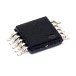
| 描述 | ADC 16BIT 1MSPS 2.5LSB 10-MSOP |
| 产品分类 | |
| 品牌 | Analog Devices Inc |
| 数据手册 | |
| 产品图片 |
|
| 产品型号 | AD7980ARMZRL7 |
| rohs | 无铅 / 符合限制有害物质指令(RoHS)规范要求 |
| 产品系列 | PulSAR® |
| 产品目录页面 | |
| 位数 | 16 |
| 供应商器件封装 | 10-MSOP |
| 其它名称 | AD7980ARMZRL7CT |
| 包装 | 剪切带 (CT) |
| 安装类型 | 表面贴装 |
| 封装/外壳 | 10-TFSOP,10-MSOP(0.118",3.00mm 宽) |
| 工作温度 | -40°C ~ 125°C |
| 数据接口 | DSP,MICROWIRE™,QSPI™,串行,SPI™ |
| 标准包装 | 1 |
| 特性 | - |
| 电压源 | 单电源 |
| 转换器数 | 1 |
| 输入数和类型 | 1 个伪差分,单极 |
| 配用 | /product-detail/zh/EVAL-AD7980-PMDZ/EVAL-AD7980-PMDZ-ND/4875931 |
| 采样率(每秒) | 1M |


- 商务部:美国ITC正式对集成电路等产品启动337调查
- 曝三星4nm工艺存在良率问题 高通将骁龙8 Gen1或转产台积电
- 太阳诱电将投资9.5亿元在常州建新厂生产MLCC 预计2023年完工
- 英特尔发布欧洲新工厂建设计划 深化IDM 2.0 战略
- 台积电先进制程称霸业界 有大客户加持明年业绩稳了
- 达到5530亿美元!SIA预计今年全球半导体销售额将创下新高
- 英特尔拟将自动驾驶子公司Mobileye上市 估值或超500亿美元
- 三星加码芯片和SET,合并消费电子和移动部门,撤换高东真等 CEO
- 三星电子宣布重大人事变动 还合并消费电子和移动部门
- 海关总署:前11个月进口集成电路产品价值2.52万亿元 增长14.8%


PDF Datasheet 数据手册内容提取
16-Bit, 1 MSPS, PulSAR ADC in MSOP/LFCSP Data Sheet AD7980 FEATURES TYPICAL APPLICATION CIRCUIT 16-bit resolution with no missing codes 2.5VTO 5V 2.5V Throughput: 1 MSPS Low power dissipation 4 mW at 1 MSPS (VDD only) REF VDD VIO 1.8VTO 5.0V 0TO VREF 7 mW at 1 MSPS (total) SDI IN+ 70 µW at 10 kSPS AD7980SCK 3- OR 4-WIRE INTERFACE IN– SDO (SPI, DAISY CHAIN, CS) INL: ±0.6 LSB typical, ±1.25 LSB maximum TSHINDA:D −:1 9110. 2d5B d aBt 1a0t 1k0H kzH z GND CNV 06392-001 Figure 1. Pseudo differential analog input range 0 V to V with V between 2.5 V to 5 V GENERAL DESCRIPTION REF REF No pipeline delay The AD79801 is a 16-bit, successive approximation, analog-to- Single-supply 2.5 V operation with 1.8 V/2.5 V/3 V/5 V digital converter (ADC) that operates from a single power supply, logic interface VDD. It contains a low power, high speed, 16-bit sampling ADC Proprietary serial interface and a versatile serial interface port. On the CNV rising edge, it SPI/QSPI/MICROWIRE™/DSP compatible samples an analog input, IN+, between 0 V to REF with respect Daisy-chain multiple ADCs and busy indicator to a ground sense, IN−. The reference voltage, REF, is applied 10-lead MSOP and 10-lead, 3 mm × 3 mm LFCSP, externally and can be set independent of the supply voltage, same space as SOT-23 VDD. Its power scales linearly with throughput. Wide operating temperature range: −40°C to +125°C The SPI-compatible serial interface also features the ability, APPLICATIONS using the SDI input, to daisy-chain several ADCs on a single, Battery-powered equipment 3-wire bus and provides an optional busy indicator. It is compatible Communications with 1.8 V, 2.5 V, 3 V, or 5 V logic, using the separate supply VIO. Automatic test equipment (ATE) The AD7980 is housed in a 10-lead MSOP or a 10-lead LFCSP Data acquisitions with operation specified from −40°C to +125°C. Medical instruments 1 Protected by U.S. Patent 6,703,961. Table 1. MSOP, LFCSP 14-/16-/18-/20-Bit Precision SAR ADCs and Integrated SAR ADC µModules µModule Data Type 100 kSPS 250 kSPS 400 kSPS to 500 kSPS ≥1000 kSPS Acquisition System 20-Bit AD40201 18-Bit AD7989-11 AD76911 AD40111 AD40031 AD76901 AD40071 AD7989-51 AD79821 AD79841 16-Bit AD7680 AD76851 AD76861 AD40011 ADAQ7980 AD7683 AD76871 AD76881 AD40051 ADAQ7988 AD7684 AD7694 AD76931 AD40001 AD7988-11 AD7988-51 AD40041 AD79161 AD79801 AD40081 AD79831 14-Bit AD7940 AD79421 AD79461 1 Pin for pin compatible. Rev. F Document Feedback Information furnished by Analog Devices is believed to be accurate and reliable. However, no responsibility is assumed by Analog Devices for its use, nor for any infringements of patents or other One Technology Way, P.O. Box 9106, Norwood, MA 02062-9106, U.S.A. rights of third parties that may result from its use. Specifications subject to change without notice. No license is granted by implication or otherwise under any patent or patent rights of Analog Devices. Tel: 781.329.4700 ©2007–2017 Analog Devices, Inc. All rights reserved. Trademarks and registered trademarks are the property of their respective owners. Technical Support www.analog.com
AD7980 Data Sheet TABLE OF CONTENTS Features .............................................................................................. 1 Driver Amplifier Choice ........................................................... 16 Applications ....................................................................................... 1 Voltage Reference Input ............................................................ 17 Typical Application Circuit ............................................................. 1 Power Supply ............................................................................... 17 General Description ......................................................................... 1 Digital Interface .......................................................................... 17 Revision History ............................................................................... 2 3-Wire CS Mode Without Busy Indicator .............................. 18 Specifications ..................................................................................... 3 3-Wire CS Mode with Busy Indicator ..................................... 19 Timing Specifications .................................................................. 5 4-Wire CS Mode Without Busy Indicator .............................. 20 Absolute Maximum Ratings ............................................................ 7 4-Wire CS Mode with Busy Indicator ..................................... 21 ESD Caution .................................................................................. 7 Chain Mode Without Busy Indicator ...................................... 22 Pin Configurations and Function Descriptions ........................... 8 Chain Mode with Busy Indicator ............................................. 23 Terminology ...................................................................................... 9 Applications Information .............................................................. 24 Typical Performance Characteristics ........................................... 10 Layout .......................................................................................... 24 Theory of Operation ...................................................................... 14 Evaluating the Performance of the AD7980 .............................. 24 Circuit Information .................................................................... 14 Outline Dimensions ....................................................................... 25 Converter Operation .................................................................. 14 Ordering Guide .......................................................................... 26 Typical Application Circuit with Multiple Supplies ............... 15 Analog Input ............................................................................... 16 REVISION HISTORY 10/2017—Rev. E to Rev. F Changes to AC Accuracy Parameter, Table 2 ................................ 3 Changes to Table 1 ............................................................................ 1 Change to Standby Current Parameter, Table 3 ............................ 4 Changes to Figure 5 .......................................................................... 8 Changes to Figure 25...................................................................... 13 Updated Outline Dimensions ....................................................... 26 Changes to Table 8 .......................................................................... 15 Changes to Ordering Guide .......................................................... 26 Changes to Power Supply Section ................................................ 16 7/2016—Rev. D to Rev. E 8/2013—Rev. B to Rev. C Changed VIO = 2.3 V to 5.5 V to VIO = 1.71 V to Change to Features Section .............................................................. 1 5.5 V................................................................................. Throughout Changes to Table 3 ............................................................................. 4 Change to Features Section ............................................................. 1 Change to Figure 5 ............................................................................ 7 Changes to Conversion Rate Parameter, Table 2 .......................... 3 Added EPAD Row, Table 6 ............................................................... 7 Changes to VIO Parameter, Table 3 ............................................... 4 Changes to Evaluating the Performance of the Deleted VIO Range Parameter, Table 3 ......................................... 4 AD7980 Section .............................................................................. 23 Added Table 5; Renumbered Sequentially .................................... 6 Updated Outline Dimensions ....................................................... 24 Changes to Table 7 ............................................................................ 8 Changes to Ordering Guide .......................................................... 25 Changes to Table 9 .......................................................................... 16 Changes to Voltage Reference Input Section .............................. 17 6/2009—Rev. A to Rev. B Changes to Figure 32 ...................................................................... 18 Changes to Table 5 ............................................................................. 6 Changes to Figure 34 ...................................................................... 19 Changes to Figure 25...................................................................... 13 Changes to Figure 36 ...................................................................... 20 Updated Outline Dimensions ....................................................... 24 Changes to Figure 38 ...................................................................... 21 Changes to Ordering Guide .......................................................... 25 Changes to Figure 40 ...................................................................... 22 Changes to Figure 42 ...................................................................... 23 9/2008—Rev. 0 to Rev. A Deleted QFN Endnote .................................................. Throughout 7/2014—Rev. C to Rev. D Changes to Ordering Guide .......................................................... 24 Changed QFN (LFCSP) to LFCSP .............................. Throughout Changes to Features Section and Table 1 ...................................... 1 8/2007—Revision 0: Initial Version Added Patent Note, Note 1 .............................................................. 1 Rev. F | Page 2 of 26
Data Sheet AD7980 SPECIFICATIONS VDD = 2.5 V, VIO = 1.71 V to 5.5 V, V = 5 V, T = −40°C to +125°C, unless otherwise noted. REF A Table 2. A Grade B Grade Parameter Test Conditions/Comments Min Typ Max Min Typ Max Unit RESOLUTION 16 16 Bits ANALOG INPUT Voltage Range IN+ − IN− 0 V 0 V V REF REF Absolute Input Voltage IN+ −0.1 V + 0.1 −0.1 V + 0.1 V REF REF IN− −0.1 +0.1 −0.1 +0.1 V Analog Input CMRR f = 100 kHz 60 60 dB IN Leakage Current at 25°C Acquisition phase 1 1 nA Input Impedance See the See the Analog Input section Analog Input section ACCURACY No Missing Codes 16 16 Bits Differential Linearity Error REF = 5 V −1.0 ±0.5 +2.0 −0.9 ±0.4 +0.9 LSB1 REF = 2.5 V ±0.7 ±0.55 LSB1 Integral Linearity Error REF = 5 V −2.5 ±1.5 +2.5 −1.25 ±0.6 +1.25 LSB1 REF = 2.5 V ±1.65 ±0.65 LSB1 Transition Noise REF = 5 V 0.75 0.6 LSB1 REF = 2.5 V 1.2 1.0 LSB1 Gain Error, T to T 2 ±2 ±2 LSB1 MIN MAX Gain Error Temperature Drift ±0.35 ±0.35 ppm/°C Zero Error, T to T 2 −1.0 ±0.08 +1.0 −0.5 ±0.08 +0.5 mV MIN MAX Zero Temperature Drift 0.54 0.54 ppm/°C Power Supply Sensitivity VDD = 2.5 V ± 5% ±0.1 ±0.1 LSB1 THROUGHPUT Conversion Rate VIO ≥ 2.3 V up to 85°C, VIO ≥ 0 1 0 1 MSPS 3.3 V above 85°C up to 125°C VIO ≥ 1.71 V, VIO ≤ 3.3 V up 833 833 kSPS to 125°C Transient Response Full-scale step 290 290 ns AC ACCURACY Dynamic Range V = 5 V 91 92 dB3 REF V = 2.5 V 86 87 dB3 REF Oversampled Dynamic Range f = 10 kSPS 110 111 dB3 O Signal-to-Noise Ratio, SNR f = 10 kHz, V = 5 V 90.5 90 91.5 dB3 IN REF f = 10 kHz, V = 2.5 V 86.0 87.0 dB3 IN REF Spurious-Free Dynamic Range, SFDR f = 10 kHz −103.5 −110 dB3 IN Total Harmonic Distortion, THD f = 10 kHz −101 −114 dB3 IN Signal-to-Noise-and-Distortion Ratio, f = 10 kHz, V = 5 V 90 91 dB3 IN REF SINAD f = 10 kHz, V = 2.5 V 85.5 86.5 dB3 IN REF 1 LSB means least significant bit. With the 5 V input range, 1 LSB is 76.3 µV. 2 See the Terminology section. These specifications include full temperature range variation, but not the error contribution from the external reference. 3 All specifications in dB are referred to a full-scale input FSR. Tested with an input signal at 0.5 dB below full scale, unless otherwise specified. Rev. F | Page 3 of 26
AD7980 Data Sheet VDD = 2.5 V, VIO = 1.71 V to 5.5 V, V = 5 V, T = −40°C to +125°C, unless otherwise noted. REF A Table 3. Parameter Test Conditions/Comments Min Typ Max Unit REFERENCE Voltage Range 2.4 5.1 V Load Current 1 MSPS, REF = 5 V 330 µA SAMPLING DYNAMICS −3 dB Input Bandwidth 10 MHz Aperture Delay VDD = 2.5 V 2.0 ns DIGITAL INPUTS Logic Levels V VIO > 3V –0.3 0.3 × VIO V IL V VIO > 3V 0.7 × VIO VIO + 0.3 V IH V VIO ≤ 3V –0.3 0.1 × VIO IL V VIO ≤ 3V 0.9 × VIO VIO + 0.3 µA IH I −1 +1 µA IL I −1 +1 µA IH DIGITAL OUTPUTS Data Format Serial 16 bits straight binary Pipeline Delay Conversion results available immediately after completed conversion V I = 500 µA 0.4 V OL SINK V I = −500 µA VIO − 0.3 V OH SOURCE POWER SUPPLIES VDD 2.375 2.5 2.625 V VIO 1.71 5.5 V Standby Current1, 2 VDD and VIO = 2.5 V, 25°C 0.35 μA Power Dissipation VDD = 2.625 V, V = 5 V, VIO = 3 V REF Total 10 kSPS throughput 70 µW 1 MSPS throughput, B grade 7.0 9.0 mW 1 MSPS throughput, A grade 7.0 10 mW VDD Only 4 mW REF Only 1.7 mW VIO Only 1.3 mW Energy per Conversion 7.0 nJ/sample TEMPERATURE RANGE3 Specified Performance T to T −40 +125 °C MIN MAX 1 With all digital inputs forced to VIO or GND as required. 2 During the acquisition phase. 3 Contact sales for extended temperature range. Rev. F | Page 4 of 26
Data Sheet AD7980 TIMING SPECIFICATIONS −40°C to +125°C, VDD = 2.37 V to 2.63 V, VIO = 3.3 V to 5.5 V, unless otherwise stated. See Figure 2 and Figure 3 for load conditions. Table 4. Parameter Symbol Min Typ Max Unit Conversion Time: CNV Rising Edge to Data Available t 500 710 ns CONV Acquisition Time t 290 ns ACQ Time Between Conversions t 1000 ns CYC CNV Pulse Width (CS Mode) tCNVH 10 ns SCK Period (CS Mode) tSCK ns VIO Above 4.5 V 10.5 ns VIO Above 3 V 12 ns VIO Above 2.7 V 13 ns VIO Above 2.3 V 15 ns SCK Period (Chain Mode) t ns SCK VIO Above 4.5 V 11.5 ns VIO Above 3 V 13 ns VIO Above 2.7 V 14 ns VIO Above 2.3 V 16 ns SCK Low Time t 4.5 ns SCKL SCK High Time t 4.5 ns SCKH SCK Falling Edge to Data Remains Valid t 3 ns HSDO SCK Falling Edge to Data Valid Delay t DSDO VIO Above 4.5 V 9.5 ns VIO Above 3 V 11 ns VIO Above 2.7 V 12 ns VIO Above 2.3 V 14 ns CNV or SDI Low to SDO D15 MSB Valid (CS Mode) tEN VIO Above 3 V 10 ns VIO Above 2.3 V 15 ns CNV or SDI High or Last SCK Falling Edge to SDO High Impedance (CS Mode) tDIS 20 ns SDI Valid Setup Time from CNV Rising Edge t 5 ns SSDICNV SDI Valid Hold Time from CNV Rising Edge (CS Mode) tHSDICNV 2 ns SDI Valid Hold Time from CNV Rising Edge (Chain Mode) t 0 ns HSDICNV SCK Valid Setup Time from CNV Rising Edge (Chain Mode) t 5 ns SSCKCNV SCK Valid Hold Time from CNV Rising Edge (Chain Mode) t 5 ns HSCKCNV SDI Valid Setup Time from SCK Falling Edge (Chain Mode) t 2 ns SSDISCK SDI Valid Hold Time from SCK Falling Edge (Chain Mode) t 3 ns HSDISCK SDI High to SDO High (Chain Mode with Busy Indicator) t 15 ns DSDOSDI Rev. F | Page 5 of 26
AD7980 Data Sheet −40°C to +125°C, VDD = 2.37 V to 2.63 V, VIO = 1.71 V to 3.3 V, unless otherwise stated. See Figure 2 and Figure 3 for load conditions. Table 5. Parameter Symbol Min Typ Max Unit Throughput Rate 833 kSPS Conversion Time: CNV Rising Edge to Data Available t 500 800 ns CONV Acquisition Time t 290 ns ACQ Time Between Conversions t 1.2 μs CYC CNV Pulse Width (CS Mode) tCNVH 10 ns SCK Period (CS Mode) tSCK 22 ns SCK Period (Chain Mode) t 23 ns SCK SCK Low Time t 6 ns SCKL SCK High Time t 6 ns SCKH SCK Falling Edge to Data Remains Valid t 3 ns HSDO SCK Falling Edge to Data Valid Delay t 14 21 ns DSDO CNV or SDI Low to SDO D15 MSB Valid (CS Mode) tEN 18 40 ns CNV or SDI High or Last SCK Falling Edge to SDO High Impedance (CS Mode) tDIS 20 ns SDI Valid Setup Time from CNV Rising Edge t 5 ns SSDICNV SDI Valid Hold Time from CNV Rising Edge (CS Mode) tHSDICNV 10 ns SDI Valid Hold Time from CNV Rising Edge (Chain Mode) t 0 ns HSDICNV SCK Valid Setup Time from CNV Rising Edge (Chain Mode) t 5 ns SSCKCNV SCK Valid Hold Time from CNV Rising Edge (Chain Mode) t 5 ns HSCKCNV SDI Valid Setup Time from SCK Falling Edge (Chain Mode) t 2 ns SSDISCK SDI Valid Hold Time from SCK Falling Edge (Chain Mode) t 3 ns HSDISCK SDI High to SDO High (Chain Mode with Busy Indicator) t 22 ns DSDOSDI Timing Diagrams Y% VIO1 X% VIO1 500µA IOL tDELAY tDELAY VIH2 VIH2 VIL2 VIL2 TO SDO 1.4V 20pCFL 500µA IOH 06513-002 12 FMSOPINREICM VIUIFOMIC ≤ AV 3ITH.I0 OAVNN, SXD I=MN 9A T0XA AIBMNLUDEM Y3 V .=IL 1 U0;S FEODR. S VEIOE D> I3G.0ITVA XL =IN 7P0U, TASND Y = 30. 06392-003 Figure 2. Load Circuit for Digital Interface Timing Figure 3. Voltage Levels for Timing Rev. F | Page 6 of 26
Data Sheet AD7980 ABSOLUTE MAXIMUM RATINGS Table 6. Stresses at or above those listed under Absolute Maximum Parameter Rating Ratings may cause permanent damage to the product. This is a Analog Inputs stress rating only; functional operation of the product at these IN+,1 IN−1 to GND −0.3 V to V + 0.3 V or ±130 mA or any other conditions above those indicated in the operational REF Supply Voltage section of this specification is not implied. Operation beyond REF, VIO to GND −0.3 V to +6 V the maximum operating conditions for extended periods may VDD to GND −0.3 V to +3 V affect product reliability. VDD to VIO +3 V to −6 V ESD CAUTION Digital Inputs to GND −0.3 V to VIO + 0.3 V Digital Outputs to GND −0.3 V to VIO + 0.3 V Storage Temperature Range −65°C to +150°C Junction Temperature 150°C Thermal Impedance (10-Lead MSOP) θ 200°C/W JA θ 44°C/W JC Lead Temperature Vapor Phase (60 sec) 215°C Infrared (15 sec) 220°C 1 See the Analog Input section. Rev. F | Page 7 of 26
AD7980 Data Sheet PIN CONFIGURATIONS AND FUNCTION DESCRIPTIONS REF 1 10 VIO VDD 2 9 SDI AD7980 IN+ 3 8 SCK TOP VIEW REF 1 10 VIO IN– 4 (Not to Scale) 7 SDO VDD 2 AD7980 9 SDI GND 5 6 CNV IN+ 3 TOP VIEW 8 SCK (Not to Scale) IN– 4 7 SDO NOTES GND 5 6 CNV 06392-004 1 . CTMHOEINESNT C ETOCHNTEN TEEHLCEET CEIOTXNRP IOICSSA NELOD PTEP ARRDFEOQTRUOMI RGAENNDDCT.EOS. 06392-005 Figure 4. 10-Lead MSOP Pin Configuration Figure 5. 10-Lead LFCSP Pin Configuration Table 7. Pin Function Descriptions Pin No. MSOP LFCSP Mnemonic Type1 Description 1 1 REF AI Reference Input Voltage. The REF range is from 2.4 V to 5.1 V. It is referred to the GND pin. This pin should be decoupled closely to the pin with a 10 µF capacitor. 2 2 VDD P Power Supply. 3 3 IN+ AI Analog Input. It is referred to IN−. The voltage range, for example, the difference between IN+ and IN−, is 0 V to V . REF 4 4 IN− AI Analog Input Ground Sense. To be connected to the analog ground plane or to a remote sense ground. 5 5 GND P Power Supply Ground. 6 6 CNV DI Convert Input. This input has multiple functions. On its leading edge, it initiates the conversions and selects the interface mode of the device, chain, or CS mode. In CS mode, it enables the SDO pin when low. In chain mode, the data should be read when CNV is high. 7 7 SDO DO Serial Data Output. The conversion result is output on this pin. It is synchronized to SCK. 8 8 SCK DI Serial Data Clock Input. When the device is selected, the conversion result is shifted out by this clock. 9 9 SDI DI Serial Data Input. This input provides multiple features. It selects the interface mode of the ADC as follows. Chain mode is selected if SDI is low during the CNV rising edge. In this mode, SDI is used as a data input to daisy-chain the conversion results of two or more ADCs onto a single SDO line. The digital data level on SDI is output on SDO with a delay of 16 SCK cycles. CS mode is selected if SDI is high during the CNV rising edge. In this mode, either SDI or CNV can enable the serial output signals when low; if SDI or CNV is low when the conversion is complete, the busy indicator feature is enabled. 10 10 VIO P Input/Output Interface Digital Power. Nominally at the same supply as the host interface (1.8 V, 2.5 V, 3 V, or 5 V). Not 0 EPAD Not Exposed Pad. Connect the exposed pad to GND. This connection is not required to meet applicable applicable the electrical performances. 1AI = analog input, DI = digital input, DO = digital output, and P = power. Rev. F | Page 8 of 26
Data Sheet AD7980 TERMINOLOGY Effective Resolution Integral Nonlinearity Error (INL) Effective resolution is calculated as INL refers to the deviation of each individual code from a line drawn from negative full scale through positive full scale. The Effective Resolution = log(2N/RMS Input Noise) 2 point used as negative full scale occurs ½ LSB before the first and is expressed in bits. code transition. Positive full scale is defined as a level 1½ LSB Total Harmonic Distortion (THD) beyond the last code transition. The deviation is measured from THD is the ratio of the rms sum of the first five harmonic the middle of each code to the true straight line (see Figure 26). components to the rms value of a full-scale input signal and is Differential Nonlinearity Error (DNL) expressed in dB. In an ideal ADC, code transitions are 1 LSB apart. DNL is the Dynamic Range maximum deviation from this ideal value. It is often specified in Dynamic range is the ratio of the rms value of the full scale to terms of resolution for which no missing codes are guaranteed. the total rms noise measured with the inputs shorted together. Offset Error The value for dynamic range is expressed in dB. It is measured The first transition should occur at a level ½ LSB above analog with a signal at −60 dBFS to include all noise sources and DNL ground (38.1 µV for the 0 V to 5 V range). The offset error is artifacts. the deviation of the actual transition from that point. Signal-to-Noise Ratio (SNR) Gain Error SNR is the ratio of the rms value of the actual input signal to the The last transition (from 111 … 10 to 111 … 11) should occur rms sum of all other spectral components below the Nyquist for an analog voltage 1½ LSB below the nominal full scale frequency, excluding harmonics and dc. The value for SNR is (4.999886 V for the 0 V to 5 V range). The gain error is the expressed in dB. deviation of the actual level of the last transition from the ideal Signal-to-Noise-and-Distortion Ratio (SINAD) level after the offset is adjusted out. SINAD is the ratio of the rms value of the actual input signal to Spurious-Free Dynamic Range (SFDR) the rms sum of all other spectral components below the Nyquist SFDR is the difference, in decibels (dB), between the rms frequency, including harmonics but excluding dc. The value for amplitude of the input signal and the peak spurious signal. SINAD is expressed in dB. Effective Number of Bits (ENOB) Aperture Delay ENOB is a measurement of the resolution with a sine wave Aperture delay is the measure of the acquisition performance. It input. It is expressed in bits and related to SINAD by the is the time between the rising edge of the CNV input and when following formula: the input signal is held for a conversion. ENOB = (SINAD − 1.76)/6.02 dB Transient Response Noise-Free Code Resolution Transient response is the time required for the ADC to accurately Noise-free code resolution is the number of bits beyond which acquire its input after a full-scale step function is applied. it is impossible to distinctly resolve individual codes. It is calculated as Noise-Free Code Resolution = log(2N/Peak-to-Peak Noise) 2 and is expressed in bits. Rev. F | Page 9 of 26
AD7980 Data Sheet TYPICAL PERFORMANCE CHARACTERISTICS VDD = 2.5 V, V = 5.0 V, VIO = 3.3 V, unless otherwise noted. REF 1.25 1.00 POSITIVE INL: +0.33 LSB POSITIVE INL: +0.18 LSB 1.00 NEGATIVE INL: –0.39 LSB NEGATIVE INL: –0.21 LSB 0.75 0.75 0.50 0.50 0.25 B) 0.25 B) NL (LS 0 NL (LS 0 I–0.25 D –0.25 –0.50 –0.50 –0.75 ––11..2005 06392-036 ––10..0750 06392-039 0 16384 32768 49152 65536 0 16384 32768 49152 65536 CODE CODE Figure 6. Integral Nonlinearity vs. Code, REF = 5 V Figure 9. Differential Nonlinearity vs. Code, REF = 5 V 1.25 1.00 POSITIVE INL: +0.47 LSB POSITIVE INL: +0.25 LSB 1.00 NEGATIVE INL: –0.26 LSB NEGATIVE INL: –0.22 LSB 0.75 0.75 0.50 0.50 0.25 B) 0.25 B) NL (LS 0 NL (LS 0 I–0.25 D –0.25 –0.50 –0.50 –0.75 ––11..2050 06392-060 ––10..0750 06392-061 0 16384 32768 49152 65536 0 16384 32768 49152 65536 CODE CODE Figure 7. Integral Nonlinearity vs. Code, REF = 2.5 V Figure 10. Differential Nonlinearity vs. Code, REF = 2.5 V 0 0 fS = 1 MSPS fS = 1 MSPS –20 fIN = 10kHz –20 fIN = 10kHz SNR = 91.27dB SNR = 86.8dB E) THD = –114.63dB E) THD = –111.4dB AL –40 SFDR = 110.10dB AL –40 SFDR = 105.9dB SC SINAD = 91.25dB SC SINAD = 86.8dB L –60 L –60 L L U U of F –80 of F –80 B B d –100 d –100 E ( E ( D D U –120 U –120 T T LI LI P P M –140 M –140 A A ––118600 06392-038 ––118600 06392-058 0 100 200 300 400 500 0 100 200 300 400 500 FREQUENCY (kHz) FREQUENCY (kHz) Figure 8. FFT Plot, REF = 5 V Figure 11. FFT Plot, REF = 2.5 V Rev. F | Page 10 of 26
Data Sheet AD7980 180k 60k 168591 160k 52212 50k 140k 120k 40k TS100k TS 32417 31340 UN UN 30k O 80k O C C 60k 20k 52710 40k 38751 10k 7225 6807 20k0 0 0 27 1201 829 33 2 0 0 0 06392-042 0 0 0 16 539 502 14 0 0 06392-059 8003800480058006800780088009800A800B800C800D800E800F 7FFA7FFB7FFC7FFD7FFE7FFF8000800180028003800480058006 CODE IN HEX CODE IN HEX Figure 12. Histogram of a DC Input at the Code Center, REF = 5 V Figure 15. Histogram of a DC Input at the Code Center, REF = 2.5 V 70k 95 5969159404 94 60k 93 50k 92 91 S 40k B) UNT R (d 90 O N C 30k S 89 20k 88 87 10k0 0 2 150 5428 6295 93 3 0 06392-043 8856 06392-046 7FFF 8000 8001 8002 8003 8004 8005 8006 8007 8008 –10 –9 –8 –7 –6 –5 –4 –3 –2 –1 0 CODE IN HEX INPUT LEVEL (dB OF FULL SCALE) Figure 13. Histogram of a DC Input at the Code Transition, REF = 5 V Figure 16. SNR vs. Input Level 100 16 –95 115 SNR SINAD ENOB –100 SFDR 110 95 15 B) –105 105 NR, SINAD (d 90 14 ENOB (BITS) THD (dB)–110 100 SFDR (dB) S –115 THD 95 85 13 –120 90 80 12 06392-044 –125 85 06392-047 2.25 2.75 3.25 3.75 4.25 4.75 5.25 2.25 2.75 3.25 3.75 4.25 4.75 5.25 REFERENCE VOLTAGE (V) REFERENCE VOLTAGE (V) Figure 14. SNR, SINAD, and ENOB vs. Reference Voltage Figure 17. THD, SFDR vs. Reference Voltage Rev. F | Page 11 of 26
AD7980 Data Sheet 100 –85 –90 95 –95 –100 dB) B) AD ( 90 D (d–105 N H SI T –110 85 –115 80 06392-063 ––112205 06392-064 10 100 1000 10 100 1000 FREQUENCY (kHz) FREQUENCY (kHz) Figure 18. SINAD vs. Frequency Figure 21. THD vs. Frequency 95 –110 93 –112 91 –114 B) B) d d R ( D ( N H S 89 T–116 87 –118 85 06392-049 –120 06392-052 –55 –35 –15 5 25 45 65 85 105 125 –55 –35 –15 5 25 45 65 85 105 125 TEMPERATURE (°C) TEMPERATURE (°C) Figure 19. SNR vs. Temperature Figure 22. THD vs. Temperature 1.4 1.4 IVDD IVDD 1.2 1.2 1.0 1.0 A) A) T (m 0.8 T (m 0.8 N N E E CURR 0.6 IREF CURR 0.6 IREF 0.4 0.4 IVIO IVIO 0.2 0.2 0 06392-050 0 06392-053 2.375 2.425 2.475 2.525 2.575 2.625 –55 –35 –15 5 25 45 65 85 105 125 VDD VOLTAGE (V) TEMPERATURE (°C) Figure 20. Operating Currents vs. Supply Figure 23. Operating Currents vs. Temperature Rev. F | Page 12 of 26
Data Sheet AD7980 8 7 6 A) 5 µ T ( EN 4 RR U C 3 IVDD + IVIO 2 10 06392-054 –55 –35 –15 5 25 45 65 85 105 125 TEMPERATURE (°C) Figure 24. Power-Down Currents vs. Temperature Rev. F | Page 13 of 26
AD7980 Data Sheet THEORY OF OPERATION IN+ MSB SWITCHES CONTROL LSB SW+ 32,768C 16,384C 4C 2C C C BUSY REF COMP CONTROL LOGIC GND OUTPUT CODE 32,768C 16,384C 4C 2C C C LSB SW+ MSB CNV IN– 06392-011 Figure 25. ADC Simplified Schematic CIRCUIT INFORMATION During the acquisition phase, terminals of the array tied to the input of the comparator are connected to GND via SW+ and The AD7980 is a fast, low power, single-supply, precise 16-bit SW−. All independent switches are connected to the analog inputs. ADC that uses a successive approximation architecture. Therefore, the capacitor arrays are used as sampling capacitors The AD7980 is capable of converting 1,000,000 samples per and acquire the analog signal on the IN+ and IN− inputs. When second (1 MSPS) and powers down between conversions. When the acquisition phase is completed and the CNV input goes high, operating at 10 kSPS, for example, it consumes 70 µW typically, a conversion phase is initiated. When the conversion phase begins, ideal for battery-powered applications. SW+ and SW− are opened first. The two capacitor arrays are then The AD7980 provides the user with on-chip track-and-hold disconnected from the inputs and connected to the GND input. and does not exhibit any pipeline delay or latency, making it Therefore, the differential voltage between the inputs IN+ and ideal for multiple multiplexed channel applications. IN− captured at the end of the acquisition phase are applied to the comparator inputs, causing the comparator to become The AD7980 can be interfaced to any 1.8 V to 5 V digital logic unbalanced. By switching each element of the capacitor array family. It is housed in a 10-lead MSOP or a tiny 10-lead LFCSP between GND and REF, the comparator input varies by binary that combines space savings and allows flexible configurations. weighted voltage steps (V /2, V /4 … V /65,536). The control REF REF REF It is pin-for-pin compatible with the 18-bit AD7982. logic toggles these switches, starting with the MSB, to bring the CONVERTER OPERATION comparator back into a balanced condition. After the completion of this process, the device returns to the acquisition phase and the The AD7980 is a successive approximation ADC based on a control logic generates the ADC output code and a busy signal charge redistribution DAC. Figure 25 shows the simplified indicator. schematic of the ADC. The capacitive DAC consists of two identical arrays of 16 binary weighted capacitors, which are Because the AD7980 has an on-board conversion clock, the connected to the two comparator inputs. serial clock, SCK, is not required for the conversion process. Rev. F | Page 14 of 26
Data Sheet AD7980 Transfer Functions Table 8. Output Codes and Ideal Input Voltages The ideal transfer characteristic for the AD7980 is shown in Analog Input Figure 26 and Table 8. Description VREF = 5 V Digital Output Code (Hex) FSR − 1 LSB 4.999924 V FFFF1 Midscale + 1 LSB 2.500076 V 8001 111 ...111 Midscale 2.5 V 8000 ARY)111111 ...... 111001 Midscale − 1 LSB 2.499924 V 7FFF BIN −FSR + 1 LSB 76.3 µV 0001 HT −FSR 0 V 00002 G AI TR 1 This is also the code for an overranged analog input (VIN+ − VIN− above VREF − VGND). E (S 2 This is also the code for an underranged analog input (VIN+ − VIN− below VGND). D O TYPICAL APPLICATION CIRCUIT WITH MULTIPLE C DC SUPPLIES A 000 ... 010 Figure 27 shows an example of a typical application circuit for 000 ... 001 the AD7980 when multiple supplies are available. 000 ... 000 –FSR –FSR + 1LSB +FSR – 1 LSB –FSR + 0.5LSB ANALOG INP+UFTSR – 1.5 LSB 06392-012 Figure 26. ADC Ideal Transfer Function V+ REF1 2.5V 10µF2 100nF V+ 1.8VTO 5V 20Ω 100nF 0TO VREF REF VDD VIO SDI IN+ 2.7nF V– SCK AD7980 3- OR 4-WIRE INTERFACE 4 SDO IN– CNV GND 06392-013 1SEE THE VOLTAGE REFERENCE INPUT SECTION FOR REFERENCE SELECTION. 2CREF IS USUALLY A 10µF CERAMIC CAPACITOR (X5R). 3SEE THE DRIVERAMPLIFIER CHOICE SECTION. 4OPTIONAL FILTER. SEE THEANALOG INPUT SECTION. 5SEE THE DIGITAL INTERFACE FOR THE MOST CONVENIENT INTERFACE MODE. Figure 27. Typical Application Circuit with Multiple Supplies Rev. F | Page 15 of 26
AD7980 Data Sheet ANALOG INPUT DRIVER AMPLIFIER CHOICE Figure 28 shows an equivalent circuit of the input structure of Although the AD7980 is easy to drive, the driver amplifier the AD7980. needs to meet the following requirements: The two diodes, D1 and D2, provide ESD protection for the The noise generated by the driver amplifier needs to be analog inputs, IN+ and IN−. Care must be taken to ensure that kept as low as possible to preserve the SNR and transition the analog input signal never exceeds the supply rails by more noise performance of the AD7980. The noise coming from than 0.3 V, because this causes these diodes to become forward- the driver is filtered by the 1-pole, low-pass filter of the biased and start conducting current. These diodes can handle a AD7980 analog input circuit made by R and C or by the IN IN forward-biased current of 130 mA maximum. For instance, external filter, if one is used. Because the typical noise of the these conditions could eventually occur when the supplies of AD7980 is 47.3 μV rms, the SNR degradation due to the the input buffer (U1) are different from VDD. In such a case amplifier is (for example, an input buffer with a short circuit), the current limitation can be used to protect the device. 47.3 REF SNR 20log LOSS π 47.32 f (Ne )2 IN+ D1 RIN CIN 2 3dB N OR IN– where: CPIN D2 f is the input bandwidth in MHz of the AD7980 GND 06392-014 (–130dB MHz) or the cutoff frequency of the input filter, if Figure 28. Equivalent Analog Input Circuit one is used. N is the noise gain of the amplifier (for example, 1 in buffer The analog input structure allows the sampling of the true configuration). differential signal between IN+ and IN−. By using these e is the equivalent input noise voltage of the op amp, N differential inputs, signals common to both inputs are rejected. in nV/√Hz. During the acquisition phase, the impedance of the analog For ac applications, the driver should have a THD inputs (IN+ and IN−) can be modeled as a parallel combination of performance commensurate with the AD7980. capacitor, C , and the network formed by the series connection of PIN For multichannel multiplexed applications, the driver R and C . C is primarily the pin capacitance. R is typically IN IN PIN IN amplifier and the AD7980 analog input circuit must settle 400 Ω and is a lumped component made up of some serial for a full-scale step onto the capacitor array at a 16-bit level resistors and the on resistance of the switches. C is typically IN (0.0015%, 15 ppm). In the amplifier data sheet, settling at 30 pF and is mainly the ADC sampling capacitor. During the 0.1% to 0.01% is more commonly specified. This can differ conversion phase, where the switches are opened, the input significantly from the settling time at a 16-bit level and impedance is limited to C . R and C make a 1-pole, low-pass PIN IN IN should be verified prior to driver selection. filter that reduces undesirable aliasing effects and limits the noise. When the source impedance of the driving circuit is low, the Table 9. Recommended Driver Amplifiers1 AD7980 can be driven directly. Large source impedances Amplifier Typical Application significantly affect the ac performance, especially THD. The dc ADA4805-1 Low noise, small size, and low power performances are less sensitive to the input impedance. The ADA4807-1 Very low noise and high frequency maximum source impedance depends on the amount of THD ADA4627-1 Precision, low noise, and low input bias current that can be tolerated. The THD degrades as a function of the ADA4522-1 Precision, zero drift, and EMI enhanced source impedance and the maximum input frequency. ADA4500-2 Precision, rail-to-rail input/output, and zero input crossover distortion 1 For the latest recommended drivers, see the product recommendations listed on the product webpage. Rev. F | Page 16 of 26
Data Sheet AD7980 VOLTAGE REFERENCE INPUT 10.000 The AD7980 voltage reference input, REF, has a dynamic input impedance and should therefore be driven by a low impedance mA)1.000 source with efficient decoupling between the REF and GND S ( pins, as explained in the Layout section. ENT IVDD R When REF is driven by a very low impedance source, for example, UR0.100 IREF C a reference buffer using the AD8031 or the ADA4805-1, a ceramic NG IVIO chip capacitor is appropriate for optimum performance. ATI R E If an unbuffered reference voltage is used, the decoupling value P0.010 O depends on the reference used. For instance, a 22 μF (X5R, 1p2er0f6o rsmizea)n cceer uamsinicg cah liopw c atepmacpiteorra tius raep dprriofpt rAiaDteR f4o3r5 o rpetfiemreunmce . 0.001 06392-055 10000 100000 1000000 SAMPLING RATE (SPS) If desired, a reference-decoupling capacitor value as small as Figure 30. Operating Currents vs. Sampling Rate 2.2 μF can be used with a minimal impact on performance, especially DNL. DIGITAL INTERFACE Regardless, there is no need for an additional lower value ceramic Though the AD7980 has a reduced number of pins, it offers decoupling capacitor (for example, 100 nF) between the REF flexibility in its serial interface modes. and GND pins. The AD7980, when in CS mode, is compatible with SPI, QSPI™, POWER SUPPLY and digital hosts. This interface can use either a 3-wire or 4-wire interface. A 3-wire interface using the CNV, SCK, and SDO signals The AD7980 uses two power supply pins: a core supply, VDD, and minimizes wiring connections useful, for instance, in isolated a digital input/output interface supply, VIO. VIO allows direct applications. A 4-wire interface using the SDI, CNV, SCK, and interface with any logic between 1.8 V and 5.0 V. To reduce the SDO signals allows CNV, which initiates the conversions, to be number of supplies needed, VIO and VDD can be tied together. independent of the readback timing (SDI). This is useful in low The AD7980 is independent of power supply sequencing between jitter sampling or simultaneous sampling applications. VIO and VDD. Additionally, it is very insensitive to power supply variations over a wide frequency range, as shown in Figure 29. The AD7980, when in chain mode, provides a daisy-chain feature using the SDI input for cascading multiple ADCs on a 80 single data line similar to a shift register. The mode in which the device operates depends on the SDI level 75 when the CNV rising edge occurs. The CS mode is selected if SDI is high, and the chain mode is selected if SDI is low. The B) 70 SDI hold time is such that when SDI and CNV are connected d R ( together, the chain mode is selected. R S P 65 In either mode, the AD7980 offers the flexibility to optionally force a start bit in front of the data bits. This start bit can be 60 used as a busy signal indicator to interrupt the digital host and 55 06392-062 ttrhieg guesre rt hme udsatt tai mreea doiuntg t.h Oe tmhearxwimisue,m w citohnovuetr asi obnu styim ined picraiotor rt,o 1 10 100 1000 readback. FREQUENCY (kHz) The busy indicator feature is enabled in the CS mode if CNV or Figure 29. PSRR vs. Frequency SDI is low when the ADC conversion ends (see Figure 34 and The AD7980 powers down automatically at the end of each Figure 38). The busy indicator feature is enabled in the chain conversion phase and, therefore, the power scales linearly with mode if SCK is high during the CNV rising edge (see Figure 42). the sampling rate. This makes the device ideal for low sampling rate (even of a few Hz) and low battery-powered applications. Rev. F | Page 17 of 26
AD7980 Data Sheet 3-WIRE CS MODE WITHOUT BUSY INDICATOR When CNV goes low, the MSB is output onto SDO. The remaining data bits are then clocked by subsequent SCK falling This mode is usually used when a single AD7980 is connected edges. The data is valid on both SCK edges. Although the rising to an SPI-compatible digital host. The connection diagram is edge can be used to capture the data, a digital host using the shown in Figure 31, and the corresponding timing is given in SCK falling edge allows a faster reading rate provided that it has Figure 32. an acceptable hold time. After the 16th SCK falling edge or With SDI tied to VIO, a rising edge on CNV initiates a when CNV goes high, whichever is earlier, SDO returns to high conversion, selects the CS mode, and forces SDO to high impedance. impedance. Once a conversion is initiated, it continues until completion irrespective of the state of CNV. This can be useful, CONVERT for instance, to bring CNV low to select other SPI devices, such as analog multiplexers; however, CNV must be returned high CNV DIGITAL HOST before the minimum conversion time elapses and then held VIO high for the maximum conversion time to avoid the generation SDI AD7980 SDO DATA IN of the busy signal indicator. When the conversion is complete, SCK the AD7980 enters the acquisition phase and powers down. CLK 06392-015 Figure 31. 3-Wire CS Mode Without Busy Indicator Connection Diagram (SDI High) SDI = 1 tCYC tCNVH CNV tCONV tACQ AQUISITION CONVERSION AQUISITION tSCK tSCKL SCK 1 2 3 14 15 16 tHSDO tSCKH tEN tDSDO tDIS SDO D15 D14 D13 D1 D0 06392-016 Figure 32. 3-Wire CS Mode Without Busy Indicator Serial Interface Timing (SDI High) Rev. F | Page 18 of 26
Data Sheet AD7980 3-WIRE CS MODE WITH BUSY INDICATOR If multiple AD7980 devices are selected at the same time, the SDO output pin handles this contention without damage or This mode is usually used when a single AD7980 is connected induced latch-up. Meanwhile, it is recommended to keep this to an SPI-compatible digital host having an interrupt input. contention as short as possible to limit extra power dissipation. The connection diagram is shown in Figure 33, and the corresponding timing is given in Figure 34. CONVERT With SDI tied to VIO, a rising edge on CNV initiates a VIO conversion, selects the CS mode, and forces SDO to high CNV DIGITAL HOST VIO 47kΩ impedance. SDO is maintained in high impedance until the SDI AD7980 SDO DATA IN completion of the conversion irrespective of the state of CNV. Prior to the minimum conversion time, CNV can be used to SCK IRQ select other SPI devices, such as analog multiplexers, but CNV melaupsste bse a rnedtu trhneend h leolwd lboewfo froer t thhee m minaximimuumm c coonnvveersrisoionn t itmimee to CLK 06392-017 guarantee the generation of the busy signal indicator. When the Figure 33. 3-Wire CS Mode with Busy Indicator Connection Diagram (SDI High) conversion is complete, SDO goes from high impedance to low. With a pull-up on the SDO line, this transition can be used as an interrupt signal to initiate the data reading controlled by the digital host. The AD7980 then enters the acquisition phase and powers down. The data bits are clocked out, MSB first, by subsequent SCK falling edges. The data is valid on both SCK edges. Although the rising edge can be used to capture the data, a digital host using the SCK falling edge allows a faster reading rate provided it has an acceptable hold time. After the optional 17th SCK falling edge or when CNV goes high, whichever is earlier, SDO returns to high impedance. SDI = 1 tCYC tCNVH CNV tCONV tACQ AQUISITION CONVERSION AQUISITION tSCK tSCKL SCK 1 2 3 15 16 17 tHSDO tSCKH tDSDO tDIS SDO D15 D14 D1 D0 06392-018 Figure 34. 3-Wire CS Mode with Busy Indicator Serial Interface Timing (SDI High) Rev. F | Page 19 of 26
AD7980 Data Sheet 4-WIRE CS MODE WITHOUT BUSY INDICATOR When the conversion is complete, the AD7980 enters the acquisition phase and powers down. Each ADC result can be This mode is usually used when multiple AD7980 devices are read by bringing its SDI input low, which consequently outputs connected to an SPI-compatible digital host. the MSB onto SDO. The remaining data bits are then clocked by A connection diagram example using two AD7980 devices is subsequent SCK falling edges. The data is valid on both SCK shown in Figure 35, and the corresponding timing is given in edges. Although the rising edge can be used to capture the data, Figure 36. a digital host using the SCK falling edge allows a faster reading With SDI high, a rising edge on CNV initiates a conversion, rate provided it has an acceptable hold time. After the 16th SCK selects the CS mode, and forces SDO to high impedance. In this falling edge or when SDI goes high, whichever is earlier, SDO mode, CNV must be held high during the conversion phase and returns to high impedance and another AD7980 can be read. the subsequent data readback (if SDI and CNV are low, SDO is driven low). Prior to the minimum conversion time, SDI can be used to select other SPI devices, such as analog multiplexers, but SDI must be returned high before the minimum conversion time elapses and then held high for the maximum conversion time to avoid the generation of the busy signal indicator. CS2 CS1 CONVERT CNV CNV DIGITAL HOST SDI AD7980 SDO SDI AD7980 SDO SCK SCK CDLAKTA IN 06392-019 Figure 35. 4-Wire CS Mode Without Busy Indicator Connection Diagram tCYC CNV tCONV tACQ AQUISITION CONVERSION AQUISITION tSSDICNV SDI(CS1) tHSDICNV SDI(CS2) tSCK SCK tSCKL 1 2 3 14 15 16 17 18 30 31 32 tHSDO tSCKH tEN tDSDO tDIS SDO D15 D14 D13 D1 D0 D15 D14 D1 D0 06392-020 Figure 36. 4-Wire CS Mode Without Busy Indicator Serial Interface Timing Rev. F | Page 20 of 26
Data Sheet AD7980 4-WIRE CS MODE WITH BUSY INDICATOR With a pull-up on the SDO line, this transition can be used as an interrupt signal to initiate the data readback controlled by This mode is usually used when a single AD7980 is connected the digital host. The AD7980 then enters the acquisition phase to an SPI-compatible digital host that has an interrupt input, and powers down. The data bits are clocked out, MSB first, by and it is desired to keep CNV, which is used to sample the analog subsequent SCK falling edges. The data is valid on both SCK input, independent of the signal used to select the data reading. edges. Although the rising edge can be used to capture the data, This requirement is particularly important in applications where a digital host using the SCK falling edge allows a faster reading low jitter on CNV is desired. rate provided it has an acceptable hold time. After the optional The connection diagram is shown in Figure 37, and the 17th SCK falling edge or SDI going high, whichever is earlier, corresponding timing is given in Figure 38. the SDO returns to high impedance. With SDI high, a rising edge on CNV initiates a conversion, selects the CS mode, and forces SDO to high impedance. In this mode, CS1 CNV must be held high during the conversion phase and the CONVERT subsequent data readback (if SDI and CNV are low, SDO is driven VIO CNV DIGITAL HOST low). Prior to the minimum conversion time, SDI can be used 47kΩ to select other SPI devices, such as analog multiplexers, but SDI SDI AD7980 SDO DATA IN must be returned low before the minimum conversion time elapses and then held low for the maximum conversion time to SCK IRQ guarantee the generation of the busy signal indicator. When the conversion is complete, SDO goes from high impedance to low. CLK 06392-021 Figure 37. 4-Wire CS Mode with Busy Indicator Connection Diagram tCYC CNV tCONV tACQ AQUISITION CONVERSION AQUISITION tSSDICNV SDI tHSDICNV tSCK tSCKL SCK 1 2 3 15 16 17 tHSDO tSCKH tDSDO tDIS SDO tEN D15 D14 D1 D0 06392-022 Figure 38. 4-Wire CS Mode with Busy Indicator Serial Interface Timing Rev. F | Page 21 of 26
AD7980 Data Sheet CHAIN MODE WITHOUT BUSY INDICATOR readback. When the conversion is complete, the MSB is output onto SDO and the AD7980 enters the acquisition phase and This mode can be used to daisy-chain multiple AD7980 devices powers down. The remaining data bits stored in the internal on a 3-wire serial interface. This feature is useful for reducing shift register are clocked by subsequent SCK falling edges. For component count and wiring connections, for example, in each ADC, SDI feeds the input of the internal shift register and isolated multi-converter applications or for systems with a is clocked by the SCK falling edge. Each ADC in the chain limited interfacing capacity. Data readback is analogous to outputs its data MSB first, and 16 × N clocks are required to clocking a shift register. readback the N ADCs. The data is valid on both SCK edges. A connection diagram example using two AD7980s is shown in Although the rising edge can be used to capture the data, a Figure 39, and the corresponding timing is given in Figure 40. digital host using the SCK falling edge allows a faster reading When SDI and CNV are low, SDO is driven low. With SCK low, rate and, consequently, more AD7980 devices in the chain, a rising edge on CNV initiates a conversion, selects the chain provided the digital host has an acceptable hold time. The mode, and disables the busy indicator. In this mode, CNV is maximum conversion rate may be reduced due to the total held high during the conversion phase and the subsequent data readback time. CONVERT CNV CNV DIGITAL HOST SDI AD7980 SDO SDI AD7980 SDO DATA IN A B SCK SCK CLK 06392-023 Figure 39. Chain Mode Without Busy Indicator Connection Diagram SDIA = 0 tCYC CNV tCONV tACQ AQUISITION CONVERSION AQUISITION tSCK tSSCKCNV tSCKL SCK 1 2 3 14 15 16 17 18 30 31 32 tHSCKCNV tSSDISCK tSCKH tEN tHSDISC SDOA = SDIB DA15 DA14 DA13 DA1 DA0 tHSDO tDSDO SDOB DB15 DB14 DB13 DB1 DB0 DA15 DA14 DA1 DA0 06392-024 Figure 40. Chain Mode Without Busy Indicator Serial Interface Timing Rev. F | Page 22 of 26
Data Sheet AD7980 CHAIN MODE WITH BUSY INDICATOR subsequent data readback. When all ADCs in the chain have completed their conversions, the SDO pin of the ADC closest to This mode can also be used to daisy-chain multiple AD7980 the digital host (see the AD7980 ADC labeled C in Figure 41) is devices on a 3-wire serial interface while providing a busy driven high. This transition on SDO can be used as a busy indicator. This feature is useful for reducing component count indicator to trigger the data readback controlled by the digital and wiring connections, for example, in isolated multiconverter host. The AD7980 then enters the acquisition phase and powers applications or for systems with a limited interfacing capacity. down. The data bits stored in the internal shift register are Data readback is analogous to clocking a shift register. clocked out, MSB first, by subsequent SCK falling edges. For A connection diagram example using three AD7980 devices is each ADC, SDI feeds the input of the internal shift register and shown in Figure 41, and the corresponding timing is given in is clocked by the SCK falling edge. Each ADC in the chain Figure 42. outputs its data MSB first, and 16 × N + 1 clocks are required to When SDI and CNV are low, SDO is driven low. With SCK readback the N ADCs. Although the rising edge can be used to high, a rising edge on CNV initiates a conversion, selects the capture the data, a digital host using the SCK falling edge allows a chain mode, and enables the busy indicator feature. In this faster reading rate and, consequently, more AD7980 devices in mode, CNV is held high during the conversion phase and the the chain, provided the digital host has an acceptable hold time. CONVERT CNV CNV CNV DIGITAL HOST SDI AD7980 SDO SDI AD7980 SDO SDI AD7980 SDO DATA IN A B C SCK SCK SCK IRQ CLK 06392-025 Figure 41. Chain Mode with Busy Indicator Connection Diagram tCYC CNV = SDIA tCONV tACQ AQUISITION CONVERSION AQUISITION tSCK tSSCKCNV tSCKH SCK 1 2 3 4 15 16 17 18 19 31 32 33 34 35 47 48 49 tHSCKCNV tEN tSSDISCK tHSDISC tSCKL tDSDOSDI SDOA = SDIB DA15 DA14 DA13 DA1 DA0 tHSDO tDSDO tDSDOSDI SDOB = SDIC tDSDOSDI DB15 DB14 DB13 DB1 DB0 DA15 DA14 DA1 DA0 tDSDOSDI tDSDODSI SDOC DC15 DC14 DC13 DC1 DC0 DB15 DB14 DB1 DB0 DA15 DA14 DA1 DA0 06392-026 Figure 42. Chain Mode with Busy Indicator Serial Interface Timing Rev. F | Page 23 of 26
AD7980 Data Sheet APPLICATIONS INFORMATION LAYOUT AD7980 The printed circuit board (PCB) that houses the AD7980 should be designed so that the analog and digital sections are separated and confined to certain areas of the board. The pinout of the AD7980, with all its analog signals on the left side and all its digital signals on the right side, eases this task. Avoid running digital lines under the device because these couple noise onto the die, unless a ground plane under the AD7980 is used as a shield. Fast switching signals, such as CNV or clocks, should never run near analog signal paths. Crossover of digital and analog signals should be avoided. Asptl ilte absett woneee ng rtohue nddig pitlaanl aen sdh oaunladlo bge s uescetido.n It. Icna nth bee l actotmerm caosne ,o r 06392-028 Figure 43. Example Layout of the AD7980 (Top Layer) the planes should be joined underneath the AD7980 devices. The AD7980 voltage reference input REF has a dynamic input impedance and should be decoupled with minimal parasitic inductances. This is done by placing the reference decoupling ceramic capacitor close to, ideally right up against, the REF and GND pins and connecting them with wide, low impedance traces. Finally, the power supplies VDD and VIO of the AD7980 should be decoupled with ceramic capacitors, typically 100 nF, placed close to the AD7980 and connected using short and wide traces to provide low impedance paths and reduce the effect of glitches on the power supply lines. An example of a layout following these rules is shown in FEiVguArLe U43A aTnIdN FGig TuHreE 4 4P.E RFORMANCE OF THE AD7980 06392-027 Figure 44. Example Layout of the AD7980 (Bottom Layer) Other recommended layouts for the AD7980 are outlined in the documentation of the evaluation board for the AD7980 (EVAL-AD7980SDZ). The evaluation board package includes a fully assembled and tested evaluation board, documentation, and software for controlling the board from a PC via the EVAL-SDP-CB1Z. Rev. F | Page 24 of 26
Data Sheet AD7980 OUTLINE DIMENSIONS 3.10 3.00 2.90 10 6 5.15 3.10 4.90 3.00 4.65 2.90 1 5 PIN1 IDENTIFIER 0.50BSC 0.95 15°MAX 0.85 1.10MAX 0.75 0.70 0.15 0.30 6° 0.23 0.55 CO0P.0L5ANARITY 0.15 0° 0.13 0.40 0.10 COMPLIANTTOJEDECSTANDARDSMO-187-BA 091709-A Figure 45.10-Lead Mini Small Outline Package [MSOP] (RM-10) Dimensions shown in millimeters 2.48 2.38 3.10 2.23 3.00 SQ 2.90 0.50 BSC 6 10 PIN 1 INDEX EXPOSED 1.74 AREA PAD 1.64 0.50 1.49 0.40 0.30 5 1 0.20 MIN TOP VIEW BOTTOM VIEW PIN 1 INDICATOR (R 0.15) 0.80 FOR PROPER CONNECTION OF 0.75 0.05 MAX TTHHEE PEIXNP COOSNEDFI GPAUDR,A RTEIOFNE RA NTOD 0.70 0.02 NOM FUNCTION DESCRIPTIONS COPLANARITY SECTION OF THIS DATA SHEET. SEPALTAINNGE 000...322050 0.20 REF 0.08 02-05-2013-C Figure 46. 10-Lead Lead Frame Chip Scale Package [LFCSP] 3 mm × 3 mm Body and 0.75 mm Package Height (CP-10-9) Dimensions shown in millimeters Contact sales for the non-RoHS compliant version of the device. Rev. F | Page 25 of 26
AD7980 Data Sheet ORDERING GUIDE Integral Package Ordering Model1, 2, 3 Nonlinearity Temperature Range Package Description Option Branding Quantity AD7980ARMZ ±2.5 LSB max −40°C to +125°C 10-Lead MSOP RM-10 C5X Tube, 50 AD7980ARMZRL7 ±2.5 LSB max −40°C to +125°C 10-Lead MSOP RM-10 C5X Reel, 1,000 AD7980BRMZ ±1.25 LSB max −40°C to +125°C 10-Lead MSOP RM-10 C5D Tube, 50 AD7980BRMZRL7 ±1.25 LSB max −40°C to +125°C 10-Lead MSOP RM-10 C5D Reel, 1,000 AD7980ACPZ-RL ±2.5 LSB max −40°C to +125°C 10-Lead LFCSP CP-10-9 C5X Reel, 5,000 AD7980ACPZ-RL7 ±2.5 LSB max −40°C to +125°C 10-Lead LFCSP CP-10-9 C5X Reel, 1,000 AD7980BCPZ-RL ±1.25 LSB max −40°C to +125°C 10-Lead LFCSP CP-10-9 C5D Reel, 5,000 AD7980BCPZ-RL7 ±1.25 LSB max −40°C to +125°C 10-Lead LFCSP CP-10-9 C5D Reel, 1,000 AD7980BCPZ-R2 ±1.25 LSB max −40°C to +125°C 10-Lead LFCSP CP-10-9 C5D Reel, 1,000 EVAL-AD7980SDZ Evaluation Board EVAL-SDP-CB1Z Controller Board 1 Z = RoHS Compliant Part. 2 The EVAL-AD7980SDZ can be used as a standalone evaluation board or in conjunction with the EVAL-SDP-CB1Z for evaluation/demonstration purposes. 3 The EVAL-SDP-CB1Z allows a PC to control and communicate with all Analog Devices evaluation boards ending in the SD designator. ©2007–2017 Analog Devices, Inc. All rights reserved. Trademarks and registered trademarks are the property of their respective owners. D06392-0-10/17(F) Rev. F | Page 26 of 26
Mouser Electronics Authorized Distributor Click to View Pricing, Inventory, Delivery & Lifecycle Information: A nalog Devices Inc.: AD7980BRMZ AD7980ACPZ-RL AD7980ARMZ AD7980BRMZRL7 AD7980BCPZ-RL7 AD7980BCPZ-RL AD7980ACPZ-RL7 AD7980SRMZ-EP-RL7 AD7980ARMZRL7 EVAL-AD7980SDZ AD7980SRMZ-EP