ICGOO在线商城 > 集成电路(IC) > 数据采集 - 模数转换器 > TLC549IP
 Datasheet下载
- 型号: TLC549IP
- 制造商: Texas Instruments
- 库位|库存: xxxx|xxxx
- 要求:
| 数量阶梯 | 香港交货 | 国内含税 |
| +xxxx | $xxxx | ¥xxxx |
查看当月历史价格
查看今年历史价格
TLC549IP产品简介:
ICGOO电子元器件商城为您提供TLC549IP由Texas Instruments设计生产,在icgoo商城现货销售,并且可以通过原厂、代理商等渠道进行代购。 TLC549IP价格参考¥5.14-¥11.05。Texas InstrumentsTLC549IP封装/规格:数据采集 - 模数转换器, 8 Bit Analog to Digital Converter 1 Input 1 SAR 8-PDIP。您可以下载TLC549IP参考资料、Datasheet数据手册功能说明书,资料中有TLC549IP 详细功能的应用电路图电压和使用方法及教程。
TLC549IP 是由 Texas Instruments(德州仪器)生产的一款 8 位模数转换器(ADC),属于数据采集系列。它具有串行接口,适用于多种需要将模拟信号转换为数字信号的应用场景。以下是 TLC549IP 的主要应用场景:

1. 工业控制与监测
   TLC549IP 可用于工业自动化设备中的传感器信号采集。例如,温度、压力、湿度等传感器输出的模拟信号可以通过 TLC549IP 转换为数字信号,便于微控制器进行处理和分析。这种应用常见于工厂监控系统、过程控制系统以及环境监测设备。

2. 医疗设备
   在医疗领域,TLC549IP 可用于便携式健康监测设备中,如血糖仪、心率监测仪或体温计。这些设备通常需要将生物信号(如电压变化)转换为数字信号以进行显示或进一步计算。

3. 家用电子设备
   TLC549IP 可应用于家用电器中,例如智能电表、烟雾报警器或恒温器。这些设备通过 ADC 将模拟信号(如电流、电压或温度)转换为数字信号,实现精准控制和反馈。

4. 音频信号处理
   在低精度音频应用中,TLC549IP 可用于将麦克风或其他音频输入的模拟信号转换为数字信号,以便后续处理或存储。例如,简单的语音记录设备或玩具中的声音识别功能。

5. 汽车电子
   TLC549IP 可用于汽车电子系统的信号采集,例如车速传感器、油量传感器或温度传感器的数据读取。通过 ADC 转换,车辆控制系统可以实时获取关键参数并作出相应调整。

6. 消费类电子产品
   在低成本消费类电子产品中,TLC549IP 提供了一种经济高效的解决方案。例如,遥控器中的电池电压检测、触摸感应设备中的信号采集等。

总结来说,TLC549IP 的 8 位分辨率和串行接口设计使其适合对精度要求不高但成本敏感的应用场景。其简单易用的特点也使其成为许多嵌入式系统中模数转换的理想选择。
| 参数 | 数值 |
| 产品目录 | 集成电路 (IC)半导体 |
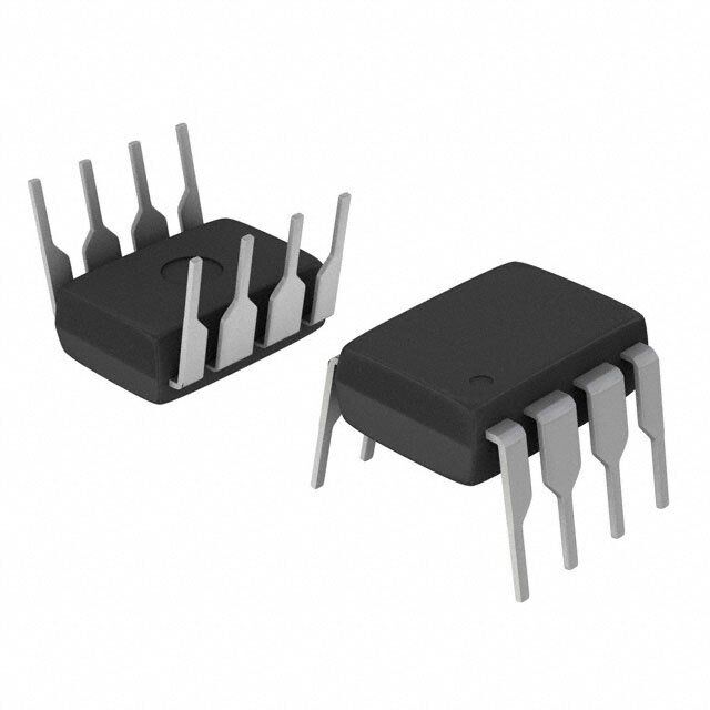
| 描述 | IC 8-BIT SERIAL CNTRL A/D 8-DIP模数转换器 - ADC 8bit A/D w/Serial |
| 产品分类 | |
| 品牌 | Texas Instruments |
| 产品手册 | |
| 产品图片 |
|
| rohs | 符合RoHS无铅 / 符合限制有害物质指令(RoHS)规范要求 |
| 产品系列 | 数据转换器IC,模数转换器 - ADC,Texas Instruments TLC549IP- |
| 数据手册 | |
| 产品型号 | TLC549IP |
| PCN设计/规格 | |
| 产品培训模块 | http://www.digikey.cn/PTM/IndividualPTM.page?site=cn&lang=zhs&ptm=13240 |
| 产品目录页面 | |
| 产品种类 | 模数转换器 - ADC |
| 位数 | 8 |
| 供应商器件封装 | 8-PDIP |
| 信噪比 | Yes |
| 其它名称 | 296-1855 |
| 分辨率 | 8 bit |
| 制造商产品页 | http://www.ti.com/general/docs/suppproductinfo.tsp?distId=10&orderablePartNumber=TLC549IP |
| 包装 | 管件 |
| 单位重量 | 440.400 mg |
| 商标 | Texas Instruments |
| 安装类型 | 通孔 |
| 安装风格 | Through Hole |
| 封装 | Tube |
| 封装/外壳 | 8-DIP(0.300",7.62mm) |
| 封装/箱体 | PDIP-8 |
| 工作温度 | -40°C ~ 85°C |
| 工作电源电压 | 3 V to 6 V |
| 工厂包装数量 | 50 |
| 接口类型 | Serial, SPI |
| 数据接口 | 串行 |
| 最大功率耗散 | 15 mW |
| 最大工作温度 | + 85 C |
| 最小工作温度 | - 40 C |
| 标准包装 | 50 |
| 特性 | - |
| 电压参考 | External |
| 电压源 | 单电源 |
| 系列 | TLC549 |
| 结构 | SAR |
| 转换器数 | 1 |
| 转换器数量 | 1 |
| 转换速率 | 40 kS/s |
| 输入数和类型 | 1 个单端,单极 |
| 输入类型 | Single-Ended |
| 通道数量 | 1 Channel |
| 采样率(每秒) | 40k |


- 商务部:美国ITC正式对集成电路等产品启动337调查
- 曝三星4nm工艺存在良率问题 高通将骁龙8 Gen1或转产台积电
- 太阳诱电将投资9.5亿元在常州建新厂生产MLCC 预计2023年完工
- 英特尔发布欧洲新工厂建设计划 深化IDM 2.0 战略
- 台积电先进制程称霸业界 有大客户加持明年业绩稳了
- 达到5530亿美元!SIA预计今年全球半导体销售额将创下新高
- 英特尔拟将自动驾驶子公司Mobileye上市 估值或超500亿美元
- 三星加码芯片和SET,合并消费电子和移动部门,撤换高东真等 CEO
- 三星电子宣布重大人事变动 还合并消费电子和移动部门
- 海关总署:前11个月进口集成电路产品价值2.52万亿元 增长14.8%


PDF Datasheet 数据手册内容提取
TLC548C, TLC548I, TLC549C, TLC549I 8-BIT ANALOG-TO-DIGITAL CONVERTERS WITH SERIAL CONTROL SLAS067C – NOVEMBER 1983 – REVISED SEPTEMBER 1996 (cid:1) Microprocessor Peripheral or Standalone D OR P PACKAGE Operation (TOP VIEW) (cid:1) 8-Bit Resolution A/D Converter (cid:1) REF+ 1 8 VCC Differential Reference Input Voltages ANALOG IN 2 7 I/O CLOCK (cid:1) Conversion Time...17 m s Max REF– 3 6 DATA OUT (cid:1) Total Access and Conversion Cycles Per GND 4 5 CS Second – TLC548...up to 45500 – TLC549...up to 40000 (cid:1) On-Chip Software-Controllable Sample-and-Hold Function (cid:1) Total Unadjusted Error...±0.5 LSB Max (cid:1) 4-MHz Typical Internal System Clock (cid:1) Wide Supply Range...3 V to 6 V (cid:1) Low Power Consumption...15 mW Max (cid:1) Ideal for Cost-Effective, High-Performance Applications including Battery-Operated Portable Instrumentation (cid:1) Pinout and Control Signals Compatible With the TLC540 and TLC545 8-Bit A/D Converters and with the TLC1540 10-Bit A/D Converter (cid:1) CMOS Technology description The TLC548 and TLC549 are CMOS analog-to-digital converter (ADC) integrated circuits built around an 8-bit switched-capacitor successive-approximation ADC. These devices are designed for serial interface with a microprocessor or peripheral through a 3-state data output and an analog input. The TLC548 and TLC549 use only the input/output clock (I/O CLOCK) input along with the chip select (CS) input for data control. The maximum I/O CLOCK input frequency of the TLC548 is 2.048 MHz, and the I/O CLOCK input frequency of the TLC549 is specified up to 1.1 MHz. AVAILABLE OPTIONS PACKAGE TA SMALL OUTLINE PLASTIC DIP (D) (P) TLC548CD TLC548CP 0°C to 70°C TLC549CD TLC549CP TLC548ID TLC548IP –40°C to 85°C TLC549ID TLC549IP Please be aware that an important notice concerning availability, standard warranty, and use in critical applications of TexasInstruments semiconductor products and disclaimers thereto appears at the end of this data sheet. PRODUCTION DATA information is current as of publication date. Copyright 1996, Texas Instruments Incorporated Products conform to specifications per the terms of Texas Instruments standard warranty. Production processing does not necessarily include testing of all parameters. POST OFFICE BOX 655303 • DALLAS, TEXAS 75265 1
TLC548C, TLC548I, TLC549C, TLC549I 8-BIT ANALOG-TO-DIGITAL CONVERTERS WITH SERIAL CONTROL SLAS067C – NOVEMBER 1983 – REVISED SEPTEMBER 1996 description (continued) Operation of the TLC548 and the TLC549 is very similar to that of the more complex TLC540 and TLC541 devices; however, the TLC548 and TLC549 provide an on-chip system clock that operates typically at 4 MHz and requires no external components. The on-chip system clock allows internal device operation to proceed independently of serial input/output data timing and permits manipulation of the TLC548 and TLC549 as desired for a wide range of software and hardware requirements. The I/O CLOCK together with the internal system clock allow high-speed data transfer and conversion rates of 45500 conversions per second for the TLC548, and 40000 conversions per second for the TLC549. Additional TLC548 and TLC549 features include versatile control logic, an on-chip sample-and-hold circuit that can operate automatically or under microprocessor control, and a high-speed converter with differential high-impedance reference voltage inputs that ease ratiometric conversion, scaling, and circuit isolation from logic and supply noises. Design of the totally switched-capacitor successive-approximation converter circuit allows conversion with a maximum total error of ±0.5 least significant bit (LSB) in less than 17 m s. The TLC548C and TLC549C are characterized for operation from 0°C to 70°C. The TLC548I and TLC549I are characterized for operation from –40°C to 85°C. functional block diagram 1 REF+ 3 8-Bit REF– Analog-to 8 Sample Digital ANALOG IN 2 Haonldd C(CSaowpnaitvcceihtroeterdsr-) ROeDugatiptsauetr 8 4 8-Stoel-e1c Dtoarta 6 DATA and OUT Driver Internal System Clock Control 5 CS Logic and 7 Output Counter I/O CLOCK typical equivalent inputs INPUT CIRCUIT IMPEDANCE DURING SAMPLING MODE INPUT CIRCUIT IMPEDANCE DURING HOLD MODE 1 k W TYP ANALOG IN ANALOG IN Ci = 60 pF TYP 5 M W TYP (equivalent input capacitance) 2 POST OFFICE BOX 655303 • DALLAS, TEXAS 75265
TLC548C, TLC548I, TLC549C, TLC549I 8-BIT ANALOG-TO-DIGITAL CONVERTERS WITH SERIAL CONTROL SLAS067C – NOVEMBER 1983 – REVISED SEPTEMBER 1996 operating sequence 1 2 3 4 5 6 7 8 1 2 3 4 5 6 7 8 I/O Don’t Care CLOCK ACcycceles Bs Sample tconv CAyccclees Cs CSyacmlep lCe tsu(CS) Cycle B (see Note A) tsu(CS) CS twH(CS) Hi-Z State Hi-Z State DATA A7 A6 A5 A4 A3 A2 A1 A0 B7 B6 B5 B4 B3 B2 B1 B0 OUT A7 B7 Previous Conversion Data A Conversion Data B MSB LSB MSB MSB LSB MSB (see Note B) ten ten NOTES: A. The conversion cycle, which requires 36 internal system clock periods (17 m s maximum), is initiated with the eighth I/O clock pulse trailing edge after CS goes low for the channel whose address exists in memory at the time. B. The most significant bit (A7) is automatically placed on the DATA OUT bus after CS is brought low. The remaining seven bits (A6–A0) are clocked out on the first seven I/O clock falling edges. B7–B0 follows in the same manner. absolute maximum ratings over operating free-air temperature range (unless otherwise noted) Supply voltage, V (see Note 1) . . . . . . . . . . . . . . . . . . . . . . . . . . . . . . . . . . . . . . . . . . . . . . . . . . . . . . . . . . 6.5 V CC Input voltage range at any input . . . . . . . . . . . . . . . . . . . . . . . . . . . . . . . . . . . . . . . . . . . . . –0.3 V to VCC + 0.3 V Output voltage range . . . . . . . . . . . . . . . . . . . . . . . . . . . . . . . . . . . . . . . . . . . . . . . . . . . . . . –0.3 V to VCC + 0.3 V Peak input current range (any input) . . . . . . . . . . . . . . . . . . . . . . . . . . . . . . . . . . . . . . . . . . . . . . . . . . . . . ±10 mA Peak total input current range (all inputs) . . . . . . . . . . . . . . . . . . . . . . . . . . . . . . . . . . . . . . . . . . . . . . . . . ±30 mA Operating free-air temperature range, T (see Note 2): TLC548C, TLC549C . . . . . . . . . . . . . 0°C to 70°C A TLC548I, TLC549I . . . . . . . . . . . . –40°C to 85°C Storage temperature range, T . . . . . . . . . . . . . . . . . . . . . . . . . . . . . . . . . . . . . . . . . . . . . . . . . . –65°C to 150°C stg Lead temperature 1,6 mm (1/16 inch) from case for 10 seconds . . . . . . . . . . . . . . . . . . . . . . . . . . . . . . . 260°C NOTES: 1. All voltage values are with respect to the network ground terminal with the REF– and GND terminals connected together, unless otherwise noted. 2. The D package is not recommended below –40°C. POST OFFICE BOX 655303 • DALLAS, TEXAS 75265 3
TLC548C, TLC548I, TLC549C, TLC549I 8-BIT ANALOG-TO-DIGITAL CONVERTERS WITH SERIAL CONTROL SLAS067C – NOVEMBER 1983 – REVISED SEPTEMBER 1996 recommended operating conditions TLC548 TLC549 UUNNIITT MIN NOM MAX MIN NOM MAX Supply voltage, VCC 3 5 6 3 5 6 V Positive reference voltage, Vref+ (see Note 3) 2.5 VCC VCC+0.1 2.5 VCC VCC+0.1 V Negative reference voltage, Vref– (see Note 3) –0.1 0 2.5 –0.1 0 2.5 V Differential reference voltage, Vref+, Vref– (see Note 3) 1 VCC VCC+0.2 1 VCC VCC+0.2 V Analog input voltage (see Note 3) 0 VCC 0 VCC V High-level control input voltage, VIH (for VCC = 4.75 V to 5.5 V) 2 2 V Low-level control input voltage, VIL (for VCC = 4.75 V to 5.5 V) 0.8 0.8 V Input/output clock frequency, fclock(I/O) (for VCC = 4.75 V to 5.5 V) 0 2.048 0 1.1 MHz Input/output clock high, twH(I/O) (for VCC = 4.75 V to 5.5 V) 200 404 ns Input/output clock low, twL(I/O) (for VCC = 4.75 V to 5.5 V) 200 404 ns Input/output clock transition time, tt(I/O) 100 100 ns (for VCC = 4.75 V to 5.5 V) (see Note 4 and Operating Sequence) Duration of CS input high state during conversion, twH(CS) 17 17 m s (for VCC = 4.75 V to 5.5 V) (see Operating Sequence) Setup time, CS low before first I/O CLOCK, tsu(CS) 1.4 1.4 m s (for VCC = 4.75 V to 5.5 V) (see Note 5) TLC548C, TLC549C 0 70 0 70 °°CC TLC548I, TLC549I –40 85 –40 85 NOTES: 3. Analog input voltages greater than that applied to REF+ convert to all ones (11111111), while input voltages less than that applied to REF– convert to all zeros (00000000). For proper operation, the positive reference voltage Vref+, must be at least 1 V greater than the negative reference voltage, Vref–. In addition, unadjusted errors may increase as the differential reference voltage, Vref+ – Vref–, falls below 4.75 V. 4. This is the time required for the I/O CLOCK input signal to fall from VIH min to VIL max or to rise from VIL max to VIH min. In the vicinity of normal room temperature, the devices function with input clock transition time as slow as 2 m s for remote data acquisition applications in which the sensor and the ADC are placed several feet away from the controlling microprocessor. 5. To minimize errors caused by noise at the CS input, the internal circuitry waits for two rising edges and one falling edge of internal system clock after CS↓ before responding to control input signals. This CS setup time is given by the ten and tsu(CS) specifications. 4 POST OFFICE BOX 655303 • DALLAS, TEXAS 75265
TLC548C, TLC548I, TLC549C, TLC549I 8-BIT ANALOG-TO-DIGITAL CONVERTERS WITH SERIAL CONTROL SLAS067C – NOVEMBER 1983 – REVISED SEPTEMBER 1996 electrical characteristics over recommended operating free-air temperature range, V = V = 4.75 V to 5.5 V, f = 2.048 MHz for TLC548 or 1.1 MHz for TLC549 CC ref+ clock(I/O) (unless otherwise noted) PARAMETER TEST CONDITIONS MIN TYP† MAX UNIT VOH High-level output voltage VCC = 4.75 V, IOH = –360 m A 2.4 V VOL Low-level output voltage VCC = 4.75 V, IOL = 3.2 mA 0.4 V VO = VCC, CS at VCC 10 IIOOZZ HHiigghh-iimmppeeddaannccee ooffff-ssttaattee oouuttppuutt ccuurrrreenntt mm AA VO = 0, CS at VCC –10 IIH High-level input current, control inputs VI = VCC 0.005 2.5 m A IIL Low-level input current, control inputs VI = 0 –0.005 –2.5 m A Analogg channel on-state input current duringg sample Analog input at VCC 0.4 1 IIII((on)) mm AA cycle Analog input at 0 V –0.4 –1 ICC Operating supply current CS at 0 V 1.8 2.5 mA ICC + Iref Supply and reference current Vref+ = VCC 1.9 3 mA Analog inputs 7 55 CCii IInnppuutt ccaappaacciittaannccee ppFF Control inputs 5 15 operating characteristics over recommended operating free-air temperature range, V = V = 4.75 V to 5.5 V, f = 2.048 MHz for TLC548 or 1.1 MHz for TLC549 CC ref+ clock(I/O) (unless otherwise noted) TLC548 TLC549 PPAARRAAMMEETTEERR TTEESSTT CCOONNDDIITTIIOONNSS UUNNIITT MIN TYP† MAX MIN TYP† MAX EL Linearity error See Note 6 ±0.5 ±0.5 LSB EZS Zero-scale error See Note 7 ±0.5 ±0.5 LSB EFS Full-scale error See Note 7 ±0.5 ±0.5 LSB Total unadjusted error See Note 8 ±0.5 ±0.5 LSB tconv Conversion time See Operating Sequence 8 17 12 17 m s Total access and conversion time See Operating Sequence 12 22 19 25 m s I/O ta Channel acquisition time (sample cycle) See Operating Sequence 4 4 clock cycles Time output data remains tv valid after I/O CLOCK↓ 10 10 ns td Delay time to data output valid I/O CLOCK↓ 200 400 ns ten Output enable time 1.4 1.4 m s tdis Output disable time 150 150 ns tr(bus) Data bus rise time See Figure 1 300 300 ns tf(bus) Data bus fall time 300 300 ns †All typicals are at VCC = 5 V, TA = 25°C. NOTES: 6. Linearity error is the deviation from the best straight line through the A/D transfer characteristics. 7. Zero-scale error is the difference between 00000000 and the converted output for zero input voltage; full-scale error is the difference between 11111111 and the converted output for full-scale input voltage. 8. Total unadjusted error is the sum of linearity, zero-scale, and full-scale errors. POST OFFICE BOX 655303 • DALLAS, TEXAS 75265 5
TLC548C, TLC548I, TLC549C, TLC549I 8-BIT ANALOG-TO-DIGITAL CONVERTERS WITH SERIAL CONTROL SLAS067C – NOVEMBER 1983 – REVISED SEPTEMBER 1996 PARAMETER MEASUREMENT INFORMATION 1.4 V VCC 3 kW 3 kW Output Test Under Test Point Output Test Output Test Under Test Point Under Test Point CL 3 kW CL CL (see Note A) (see Note A) (see Note A) See Note B See Note B LOAD CIRCUIT FOR LOAD CIRCUIT FOR td, tr, AND tf tPZH AND tPHZ LOAD CIRCUIT FOR tPZL AND tPLZ VCC CS 50% 50% 0 V tPZL tPLZ VCC Output Waveform 1 50% (see Note C) 10% 0 V tPZH tPHZ VOH Output Waveform 2 90% 50% (see Note C) See Note B 0 V VOLTAGE WAVEFORMS FOR ENABLE AND DISABLE TIMES I/O CLOCK 0.8 V 2.4 V Output 0.4 V td tr(bus) tf(bus) 2.4 V DATA OUT 0.8 V VOLTAGE WAVEFORMS FOR RISE AND FALL TIMES VOLTAGE WAVEFORMS FOR DELAY TIME NOTES: A. CL = 50 pF for TLC548 and 100 pF for TLC549; CL includes jig capacitance. B. ten = tPZH or tPZL, tdis = tPHZ or tPLZ. C. Waveform 1 is for an output with internal conditions such that the output is low except when disabled by the output control. Waveform 2 is for an output with internal conditions such that the output is high except when disabled by the output control. Figure 1. Load Circuits and Voltage Waveforms 6 POST OFFICE BOX 655303 • DALLAS, TEXAS 75265
TLC548C, TLC548I, TLC549C, TLC549I 8-BIT ANALOG-TO-DIGITAL CONVERTERS WITH SERIAL CONTROL SLAS067C – NOVEMBER 1983 – REVISED SEPTEMBER 1996 APPLICATIONS INFORMATION simplified analog input analysis Using the equivalent circuit in Figure 2, the time required to charge the analog input capacitance from 0 to V S within 1/2 LSB can be derived as follows: The capacitance charging voltage is given by ( – t / RC ) V = V 1–e c t i (1) C S where R = R + r t s i The final voltage to 1/2 LSB is given by V (1/2 LSB) = V – (V /512) (2) C S S Equating equation 1 to equation 2 and solving for time t gives c ( – t / RC ) V –(V /512) = V 1–e c t i (3) S S S and t (1/2 LSB) = R × C × ln(512) (4) c t i Therefore, with the values given the time for the analog input signal to settle is t (1/2 LSB) = (R + 1 kW ) × 60 pF × ln(512) (5) c s This time must be less than the converter sample time shown in the timing diagrams. Driving Source† TLC548/9 Rs VI ri VS VC 1 kW MAX Ci 55 pF MAX VI = Input Voltage at ANALOG IN VS= External Driving Source Voltage Rs= Source Resistance ri = Input Resistance Ci = Input Capacitance †Driving source requirements: • Noise and distortion for the source must be equivalent to the resolution of the converter. • Rs must be real at the input frequency. Figure 2. Equivalent Input Circuit Including the Driving Source POST OFFICE BOX 655303 • DALLAS, TEXAS 75265 7
TLC548C, TLC548I, TLC549C, TLC549I 8-BIT ANALOG-TO-DIGITAL CONVERTERS WITH SERIAL CONTROL SLAS067C – NOVEMBER 1983 – REVISED SEPTEMBER 1996 PRINCIPLES OF OPERATION The TLC548 and TLC549 are each complete data acquisition systems on a single chip. Each contains an internal system clock, sample-and-hold function, 8-bit A/D converter, data register, and control logic circuitry. For flexibility and access speed, there are two control inputs: I/O CLOCK and chip select (CS). These control inputs and a TTL-compatible 3-state output facilitate serial communications with a microprocessor or minicomputer. A conversion can be completed in 17 m s or less, while complete input-conversion-output cycles can be repeated in 22 m s for the TLC548 and in 25 m s for the TLC549. The internal system clock and I/O CLOCK are used independently and do not require any special speed or phase relationships between them. This independence simplifies the hardware and software control tasks for the device. Due to this independence and the internal generation of the system clock, the control hardware and software need only be concerned with reading the previous conversion result and starting the conversion by using the I/O clock. In this manner, the internal system clock drives the “conversion crunching” circuitry so that the control hardware and software need not be concerned with this task. When CS is high, DATA OUT is in a high-impedance condition and I/O CLOCK is disabled. This CS control function allows I/O CLOCK to share the same control logic point with its counterpart terminal when additional TLC548 and TLC549 devices are used. This also serves to minimize the required control logic terminals when using multiple TLC548 and TLC549 devices. The control sequence has been designed to minimize the time and effort required to initiate conversion and obtain the conversion result. A normal control sequence is: 1. CS is brought low. To minimize errors caused by noise at CS, the internal circuitry waits for two rising edges and then a falling edge of the internal system clock after a CS↓ before the transition is recognized. However, upon a CS rising edge, DATA OUT goes to a high-impedance state within the specified t even though the dis rest of the integrated circuitry does not recognize the transition until the specified t has elapsed. This su(CS) technique protects the device against noise when used in a noisy environment. The most significant bit (MSB) of the previous conversion result initially appears on DATA OUT when CS goes low. 2. The falling edges of the first four I/O CLOCK cycles shift out the second, third, fourth, and fifth most significant bits of the previous conversion result. The on-chip sample-and-hold function begins sampling the analog input after the fourth high-to-low transition of I/O CLOCK. The sampling operation basically involves the charging of internal capacitors to the level of the analog input voltage. 3. Three more I/O CLOCK cycles are then applied to the I/O CLOCK terminal and the sixth, seventh, and eighth conversion bits are shifted out on the falling edges of these clock cycles. 4. The final (the eighth) clock cycle is applied to I/O CLOCK. The on-chip sample-and-hold function begins the hold operation upon the high-to-low transition of this clock cycle. The hold function continues for the next four internal system clock cycles, after which the holding function terminates and the conversion is performed during the next 32 system clock cycles, giving a total of 36 cycles. After the eighth I/O CLOCK cycle, CS must go high or the I/O clock must remain low for at least 36 internal system clock cycles to allow for the completion of the hold and conversion functions. CS can be kept low during periods of multiple conversion. When keeping CS low during periods of multiple conversion, special care must be exercised to prevent noise glitches on the I/O CLOCK line. If glitches occur on I/O CLOCK, the I/O sequence between the microprocessor/controller and the device loses synchronization. When CS is taken high, it must remain high until the end of conversion. Otherwise, a valid high-to-low transition of CS causes a reset condition, which aborts the conversion in progress. A new conversion may be started and the ongoing conversion simultaneously aborted by performing steps 1 through 4 before the 36 internal system clock cycles occur. Such action yields the conversion result of the previous conversion and not the ongoing conversion. 8 POST OFFICE BOX 655303 • DALLAS, TEXAS 75265
TLC548C, TLC548I, TLC549C, TLC549I 8-BIT ANALOG-TO-DIGITAL CONVERTERS WITH SERIAL CONTROL SLAS067C – NOVEMBER 1983 – REVISED SEPTEMBER 1996 PRINCIPLES OF OPERATION For certain applications, such as strobing applications, it is necessary to start conversion at a specific point in time. This device accommodates these applications. Although the on-chip sample-and-hold function begins sampling upon the high-to-low transition of the fourth I/O CLOCK cycle, the hold function does not begin until the high-to-low transition of the eighth I/O CLOCK cycle, which should occur at the moment when the analog signal must be converted. The TLC548 and TLC549 continue sampling the analog input until the high-to-low transition of the eighth I/O CLOCK pulse. The control circuitry or software then immediately lowers I/O CLOCK and starts the holding function to hold the analog signal at the desired point in time and starts the conversion. POST OFFICE BOX 655303 • DALLAS, TEXAS 75265 9
PACKAGE OPTION ADDENDUM www.ti.com 13-Oct-2018 PACKAGING INFORMATION Orderable Device Status Package Type Package Pins Package Eco Plan Lead/Ball Finish MSL Peak Temp Op Temp (°C) Device Marking Samples (1) Drawing Qty (2) (6) (3) (4/5) TLC548CD LIFEBUY SOIC D 8 75 Green (RoHS CU NIPDAU Level-1-260C-UNLIM -40 to 85 LC548C & no Sb/Br) TLC548CDR LIFEBUY SOIC D 8 2500 Green (RoHS CU NIPDAU Level-1-260C-UNLIM LC548C & no Sb/Br) TLC548CP LIFEBUY PDIP P 8 50 Green (RoHS CU NIPDAU N / A for Pkg Type TLC548CP & no Sb/Br) TLC548ID LIFEBUY SOIC D 8 75 Green (RoHS CU NIPDAU Level-1-260C-UNLIM LC548I & no Sb/Br) TLC548IDR LIFEBUY SOIC D 8 2500 Green (RoHS CU NIPDAU Level-1-260C-UNLIM LC548I & no Sb/Br) TLC548IP LIFEBUY PDIP P 8 50 Green (RoHS CU NIPDAU N / A for Pkg Type TLC548IP & no Sb/Br) TLC549CD LIFEBUY SOIC D 8 75 Green (RoHS CU NIPDAU Level-1-260C-UNLIM -40 to 85 LC549C & no Sb/Br) TLC549CDG4 LIFEBUY SOIC D 8 75 Green (RoHS CU NIPDAU Level-1-260C-UNLIM -40 to 85 LC549C & no Sb/Br) TLC549CDR LIFEBUY SOIC D 8 2500 Green (RoHS CU NIPDAU Level-1-260C-UNLIM LC549C & no Sb/Br) TLC549CDRG4 LIFEBUY SOIC D 8 2500 Green (RoHS CU NIPDAU Level-1-260C-UNLIM LC549C & no Sb/Br) TLC549CP LIFEBUY PDIP P 8 50 Green (RoHS CU NIPDAU N / A for Pkg Type TLC549CP & no Sb/Br) TLC549ID LIFEBUY SOIC D 8 75 Green (RoHS CU NIPDAU Level-1-260C-UNLIM LC549I & no Sb/Br) TLC549IDG4 LIFEBUY SOIC D 8 75 Green (RoHS CU NIPDAU Level-1-260C-UNLIM LC549I & no Sb/Br) TLC549IDR LIFEBUY SOIC D 8 2500 Green (RoHS CU NIPDAU Level-1-260C-UNLIM LC549I & no Sb/Br) TLC549IDRG4 LIFEBUY SOIC D 8 2500 Green (RoHS CU NIPDAU Level-1-260C-UNLIM LC549I & no Sb/Br) TLC549IP LIFEBUY PDIP P 8 50 Green (RoHS CU NIPDAU N / A for Pkg Type TLC549IP & no Sb/Br) TLC549IPS LIFEBUY SO PS 8 80 Green (RoHS CU NIPDAU Level-1-260C-UNLIM Y549 & no Sb/Br) Addendum-Page 1
PACKAGE OPTION ADDENDUM www.ti.com 13-Oct-2018 Orderable Device Status Package Type Package Pins Package Eco Plan Lead/Ball Finish MSL Peak Temp Op Temp (°C) Device Marking Samples (1) Drawing Qty (2) (6) (3) (4/5) TLC549IPSR LIFEBUY SO PS 8 2000 Green (RoHS CU NIPDAU Level-1-260C-UNLIM Y549 & no Sb/Br) (1) The marketing status values are defined as follows: ACTIVE: Product device recommended for new designs. LIFEBUY: TI has announced that the device will be discontinued, and a lifetime-buy period is in effect. NRND: Not recommended for new designs. Device is in production to support existing customers, but TI does not recommend using this part in a new design. PREVIEW: Device has been announced but is not in production. Samples may or may not be available. OBSOLETE: TI has discontinued the production of the device. (2) RoHS: TI defines "RoHS" to mean semiconductor products that are compliant with the current EU RoHS requirements for all 10 RoHS substances, including the requirement that RoHS substance do not exceed 0.1% by weight in homogeneous materials. Where designed to be soldered at high temperatures, "RoHS" products are suitable for use in specified lead-free processes. TI may reference these types of products as "Pb-Free". RoHS Exempt: TI defines "RoHS Exempt" to mean products that contain lead but are compliant with EU RoHS pursuant to a specific EU RoHS exemption. Green: TI defines "Green" to mean the content of Chlorine (Cl) and Bromine (Br) based flame retardants meet JS709B low halogen requirements of <=1000ppm threshold. Antimony trioxide based flame retardants must also meet the <=1000ppm threshold requirement. (3) MSL, Peak Temp. - The Moisture Sensitivity Level rating according to the JEDEC industry standard classifications, and peak solder temperature. (4) There may be additional marking, which relates to the logo, the lot trace code information, or the environmental category on the device. (5) Multiple Device Markings will be inside parentheses. Only one Device Marking contained in parentheses and separated by a "~" will appear on a device. If a line is indented then it is a continuation of the previous line and the two combined represent the entire Device Marking for that device. (6) Lead/Ball Finish - Orderable Devices may have multiple material finish options. Finish options are separated by a vertical ruled line. Lead/Ball Finish values may wrap to two lines if the finish value exceeds the maximum column width. Important Information and Disclaimer:The information provided on this page represents TI's knowledge and belief as of the date that it is provided. TI bases its knowledge and belief on information provided by third parties, and makes no representation or warranty as to the accuracy of such information. Efforts are underway to better integrate information from third parties. TI has taken and continues to take reasonable steps to provide representative and accurate information but may not have conducted destructive testing or chemical analysis on incoming materials and chemicals. TI and TI suppliers consider certain information to be proprietary, and thus CAS numbers and other limited information may not be available for release. In no event shall TI's liability arising out of such information exceed the total purchase price of the TI part(s) at issue in this document sold by TI to Customer on an annual basis. Addendum-Page 2
PACKAGE MATERIALS INFORMATION www.ti.com 20-Dec-2018 TAPE AND REEL INFORMATION *Alldimensionsarenominal Device Package Package Pins SPQ Reel Reel A0 B0 K0 P1 W Pin1 Type Drawing Diameter Width (mm) (mm) (mm) (mm) (mm) Quadrant (mm) W1(mm) TLC548CDR SOIC D 8 2500 330.0 12.4 6.4 5.2 2.1 8.0 12.0 Q1 TLC548IDR SOIC D 8 2500 330.0 12.4 6.4 5.2 2.1 8.0 12.0 Q1 TLC549CDR SOIC D 8 2500 330.0 12.4 6.4 5.2 2.1 8.0 12.0 Q1 TLC549IDR SOIC D 8 2500 330.0 12.4 6.4 5.2 2.1 8.0 12.0 Q1 TLC549IPSR SO PS 8 2000 330.0 16.4 8.35 6.6 2.5 12.0 16.0 Q1 PackMaterials-Page1
PACKAGE MATERIALS INFORMATION www.ti.com 20-Dec-2018 *Alldimensionsarenominal Device PackageType PackageDrawing Pins SPQ Length(mm) Width(mm) Height(mm) TLC548CDR SOIC D 8 2500 340.5 338.1 20.6 TLC548IDR SOIC D 8 2500 340.5 338.1 20.6 TLC549CDR SOIC D 8 2500 340.5 338.1 20.6 TLC549IDR SOIC D 8 2500 340.5 338.1 20.6 TLC549IPSR SO PS 8 2000 367.0 367.0 38.0 PackMaterials-Page2
PACKAGE OUTLINE D0008A SOIC - 1.75 mm max height SCALE 2.800 SMALL OUTLINE INTEGRATED CIRCUIT C SEATING PLANE .228-.244 TYP [5.80-6.19] .004 [0.1] C A PIN 1 ID AREA 6X .050 [1.27] 8 1 2X .189-.197 [4.81-5.00] .150 NOTE 3 [3.81] 4X (0 -15 ) 4 5 8X .012-.020 B .150-.157 [0.31-0.51] .069 MAX [3.81-3.98] .010 [0.25] C A B [1.75] NOTE 4 .005-.010 TYP [0.13-0.25] 4X (0 -15 ) SEE DETAIL A .010 [0.25] .004-.010 0 - 8 [0.11-0.25] .016-.050 [0.41-1.27] DETAIL A (.041) TYPICAL [1.04] 4214825/C 02/2019 NOTES: 1. Linear dimensions are in inches [millimeters]. Dimensions in parenthesis are for reference only. Controlling dimensions are in inches. Dimensioning and tolerancing per ASME Y14.5M. 2. This drawing is subject to change without notice. 3. This dimension does not include mold flash, protrusions, or gate burrs. Mold flash, protrusions, or gate burrs shall not exceed .006 [0.15] per side. 4. This dimension does not include interlead flash. 5. Reference JEDEC registration MS-012, variation AA. www.ti.com
EXAMPLE BOARD LAYOUT D0008A SOIC - 1.75 mm max height SMALL OUTLINE INTEGRATED CIRCUIT 8X (.061 ) [1.55] SYMM SEE DETAILS 1 8 8X (.024) [0.6] SYMM (R.002 ) TYP [0.05] 5 4 6X (.050 ) [1.27] (.213) [5.4] LAND PATTERN EXAMPLE EXPOSED METAL SHOWN SCALE:8X SOLDER MASK SOLDER MASK METAL OPENING OPENING METAL UNDER SOLDER MASK EXPOSED METAL EXPOSED METAL .0028 MAX .0028 MIN [0.07] [0.07] ALL AROUND ALL AROUND NON SOLDER MASK SOLDER MASK DEFINED DEFINED SOLDER MASK DETAILS 4214825/C 02/2019 NOTES: (continued) 6. Publication IPC-7351 may have alternate designs. 7. Solder mask tolerances between and around signal pads can vary based on board fabrication site. www.ti.com
EXAMPLE STENCIL DESIGN D0008A SOIC - 1.75 mm max height SMALL OUTLINE INTEGRATED CIRCUIT 8X (.061 ) [1.55] SYMM 1 8 8X (.024) [0.6] SYMM (R.002 ) TYP [0.05] 5 4 6X (.050 ) [1.27] (.213) [5.4] SOLDER PASTE EXAMPLE BASED ON .005 INCH [0.125 MM] THICK STENCIL SCALE:8X 4214825/C 02/2019 NOTES: (continued) 8. Laser cutting apertures with trapezoidal walls and rounded corners may offer better paste release. IPC-7525 may have alternate design recommendations. 9. Board assembly site may have different recommendations for stencil design. www.ti.com
None
None
IMPORTANTNOTICEANDDISCLAIMER TIPROVIDESTECHNICALANDRELIABILITYDATA(INCLUDINGDATASHEETS),DESIGNRESOURCES(INCLUDINGREFERENCE DESIGNS),APPLICATIONOROTHERDESIGNADVICE,WEBTOOLS,SAFETYINFORMATION,ANDOTHERRESOURCES“ASIS” ANDWITHALLFAULTS,ANDDISCLAIMSALLWARRANTIES,EXPRESSANDIMPLIED,INCLUDINGWITHOUTLIMITATIONANY IMPLIEDWARRANTIESOFMERCHANTABILITY,FITNESSFORAPARTICULARPURPOSEORNON-INFRINGEMENTOFTHIRD PARTYINTELLECTUALPROPERTYRIGHTS. TheseresourcesareintendedforskilleddevelopersdesigningwithTIproducts.Youaresolelyresponsiblefor(1)selectingtheappropriate TIproductsforyourapplication,(2)designing,validatingandtestingyourapplication,and(3)ensuringyourapplicationmeetsapplicable standards,andanyothersafety,security,orotherrequirements.Theseresourcesaresubjecttochangewithoutnotice.TIgrantsyou permissiontousetheseresourcesonlyfordevelopmentofanapplicationthatusestheTIproductsdescribedintheresource.Other reproductionanddisplayoftheseresourcesisprohibited.NolicenseisgrantedtoanyotherTIintellectualpropertyrightortoanythird partyintellectualpropertyright.TIdisclaimsresponsibilityfor,andyouwillfullyindemnifyTIanditsrepresentativesagainst,anyclaims, damages,costs,losses,andliabilitiesarisingoutofyouruseoftheseresources. TI’sproductsareprovidedsubjecttoTI’sTermsofSale(www.ti.com/legal/termsofsale.html)orotherapplicabletermsavailableeitheron ti.comorprovidedinconjunctionwithsuchTIproducts.TI’sprovisionoftheseresourcesdoesnotexpandorotherwisealterTI’sapplicable warrantiesorwarrantydisclaimersforTIproducts. MailingAddress:TexasInstruments,PostOfficeBox655303,Dallas,Texas75265 Copyright©2019,TexasInstrumentsIncorporated