ICGOO在线商城 > 集成电路(IC) > 数据采集 - 模数转换器 > AD7266BSUZ-REEL7

 Datasheet下载
- 型号: AD7266BSUZ-REEL7
- 制造商: Analog
- 库位|库存: xxxx|xxxx
- 要求:
| 数量阶梯 | 香港交货 | 国内含税 |
| +xxxx | $xxxx | ¥xxxx |
查看当月历史价格
查看今年历史价格
AD7266BSUZ-REEL7产品简介:
ICGOO电子元器件商城为您提供AD7266BSUZ-REEL7由Analog设计生产,在icgoo商城现货销售,并且可以通过原厂、代理商等渠道进行代购。 AD7266BSUZ-REEL7价格参考。AnalogAD7266BSUZ-REEL7封装/规格:数据采集 - 模数转换器, 12 Bit Analog to Digital Converter 6, 12 Input 2 SAR 32-TQFP (7x7)。您可以下载AD7266BSUZ-REEL7参考资料、Datasheet数据手册功能说明书,资料中有AD7266BSUZ-REEL7 详细功能的应用电路图电压和使用方法及教程。
AD7266BSUZ-REEL7是Analog Devices Inc.生产的一款双通道、12位、高速、低功耗模数转换器(ADC),内置采样保持放大器和基准电压源。该器件采用逐次逼近寄存器(SAR)架构,支持最高400ksps的采样速率,具备出色的动态性能和直流精度。

其典型应用场景包括工业自动化与过程控制,如PLC(可编程逻辑控制器)中的模拟信号采集,用于监测温度、压力、流量等传感器信号;在电机控制和伺服系统中,可用于实时采集电流、电压反馈信号,实现精确闭环控制。此外,该芯片适用于便携式仪器和电池供电设备,得益于其低功耗特性(正常工作时仅几毫瓦),适合对能效要求较高的手持式数据采集设备或现场测试仪表。

AD7266BSUZ-REEL7还广泛用于医疗监测设备,如心电图机、血压监测仪等,用于将生物电信号或生理参数转换为数字信号进行处理。在通信系统中,可用于中频信号采样或监控电路中的模拟参数采集。其双通道独立输入结构支持同步采样,适合需要多路信号时间对齐的应用场合。

该器件采用20引脚TSSOP封装,工作温度范围为-40°C至+85°C,适用于工业级环境。配合单电源(2.7V至5.25V)工作,接口兼容3V/5V逻辑,便于与微控制器、DSP或FPGA连接,集成度高,外围电路简洁,有助于减小系统体积并提升可靠性。
| 参数 | 数值 |
| 产品目录 | 集成电路 (IC) |
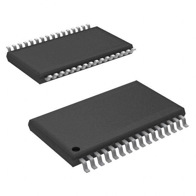
| 描述 | IC ADC 12BIT 3CHAN 2MSPS 32TQFP |
| 产品分类 | |
| 品牌 | Analog Devices Inc |
| 数据手册 | |
| 产品图片 |
|
| 产品型号 | AD7266BSUZ-REEL7 |
| rohs | 无铅 / 符合限制有害物质指令(RoHS)规范要求 |
| 产品系列 | - |
| 位数 | 12 |
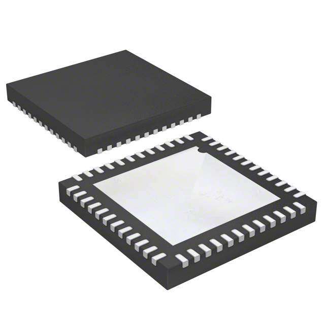
| 供应商器件封装 | 32-TQFP(7x7) |
| 其它名称 | AD7266BSUZ-REEL7-ND |
| 包装 | 剪切带 (CT) |
| 安装类型 | 表面贴装 |
| 封装/外壳 | 32-TQFP |
| 工作温度 | -40°C ~ 125°C |
| 数据接口 | DSP,MICROWIRE™,QSPI™,串行,SPI™ |
| 标准包装 | 500 |
| 特性 | 同步采样 |
| 电压源 | 模拟和数字 |
| 设计资源 | |
| 转换器数 | 2 |
| 输入数和类型 | 12 个单端,单极6 个差分,单极6 个伪差分,单极 |
| 采样率(每秒) | 2M |


- 商务部:美国ITC正式对集成电路等产品启动337调查
- 曝三星4nm工艺存在良率问题 高通将骁龙8 Gen1或转产台积电
- 太阳诱电将投资9.5亿元在常州建新厂生产MLCC 预计2023年完工
- 英特尔发布欧洲新工厂建设计划 深化IDM 2.0 战略
- 台积电先进制程称霸业界 有大客户加持明年业绩稳了
- 达到5530亿美元!SIA预计今年全球半导体销售额将创下新高
- 英特尔拟将自动驾驶子公司Mobileye上市 估值或超500亿美元
- 三星加码芯片和SET,合并消费电子和移动部门,撤换高东真等 CEO
- 三星电子宣布重大人事变动 还合并消费电子和移动部门
- 海关总署:前11个月进口集成电路产品价值2.52万亿元 增长14.8%


PDF Datasheet 数据手册内容提取
Differential/Single-Ended Input, Dual 2 MSPS, 12-Bit, 3-Channel SAR ADC AD7266 FEATURES FUNCTIONAL BLOCK DIAGRAM Dual 12-bit, 3-channel ADC REF SELECT DCAPA AVDD DVDD Throughput rate: 2 MSPS Specified for VDD of 2.7 V to 5.25 V REF BUF AD7266 Power consumption 9 mW at 1.5 MSPS with 3 V supplies VA1 VA2 27 mW at 2 MSPS with 5 V supplies 12-BIT Pin1-2c-ocnhfaignunreal bslien galnea-elongd iendp iuntpsu ts VVAA34 MUX T/H APSPURCOCAXEDISMCSAITVIEON DORUITVPEURTS DOUTA VA5 6-channel fully differential inputs SCLK VA6 CS 6-channel pseudo differential inputs RANGE 70 dB SNR at 50 kHz input frequency CONTROL SGL/DIFF LOGIC A0 Accurate on-chip reference: 2.5 V A1 ±0.2% maximum @ 25°C, 20 ppm/°C maximum VB1 A2 Dual conversion with read 437.5 ns, 32 MHz SCLK VB2 VDRIVE High speed serial interface VB3 MUX 12-BIT SPI®-/QSPI™-/MICROWIRE™-/DSP-compatible VB4 T/H APSPURCOCXEISMSAITVIEON DORUITVPEURTS DOUTB −40°C to +125°C operation VB5 ADC Shutdown mode: 1 μA maximum VB6 32-lead LFCSP and 32-lead TQFP BUF G1 MENSPESR vAerLs iDonE,S ACDR7I2P6T5I ON AGND AGND AGND DCAPB DGND DGND 04603-001 The AD72661 is a dual, 12-bit, high speed, low power, successive Figure 1. approximation ADC that operates from a single 2.7 V to 5.25 V The AD7266 is available in a 32-lead LFCSP and a power supply and features throughput rates up to 2 MSPS. The 32-lead TQFP. device contains two ADCs, each preceded by a 3-channel PRODUCT HIGHLIGHTS multiplexer, and a low noise, wide bandwidth track-and-hold 1. Two Complete ADC Functions Allow Simultaneous amplifier that can handle input frequencies in excess of 30 MHz. Sampling and Conversion of Two Channels. The conversion process and data acquisition use standard Each ADC has three fully/pseudo differential pairs, or six control inputs allowing easy interfacing to microprocessors or single-ended channels, as programmed. The conversion DSPs. The input signal is sampled on the falling edge of CS; result of both channels is simultaneously available on conversion is also initiated at this point. The conversion time is separate data lines, or in succession on one data line if only determined by the SCLK frequency. There are no pipelined one serial port is available. delays associated with the part. 2. High Throughput with Low Power Consumption. The AD7266 uses advanced design techniques to achieve very The AD7266 offers a 1.5 MSPS throughput rate with 11.4 mW low power dissipation at high throughput rates. With 5 V maximum power dissipation when operating at 3 V. supplies and a 2 MSPS throughput rate, the part consumes 3. The AD7266 offers both a standard 0 V to V input range REF 6.2 mA maximum. The part also offers flexible power/ and a 2 × V input range. REF throughput rate management when operating in normal mode 4. No Pipeline Delay. as the quiescent current consumption is so low. The part features two standard successive approximation The analog input range for the part can be selected to be a 0 V ADCs with accurate control of the sampling instant via a to VREF (or 2 × VREF) range, with either straight binary or twos CS input and once off conversion control. complement output coding. The AD7266 has an on-chip 2.5 V reference that can be overdriven when an external reference is 1 Protected by U.S. Patent No. 6,681,332 preferred. This external reference range is 100 mV to V . DD Rev. B Information furnished by Analog Devices is believed to be accurate and reliable. However, no responsibility is assumed by Analog Devices for its use, nor for any infringements of patents or other One Technology Way, P.O. Box 9106, Norwood, MA 02062-9106, U.S.A. rights of third parties that may result from its use. Specifications subject to change without notice. No license is granted by implication or otherwise under any patent or patent rights of Analog Devices. Tel: 781.329.4700 www.analog.com Trademarks and registered trademarks are the property of their respective owners. Fax: 781.461.3113 ©2005–2011 Analog Devices, Inc. All rights reserved.
AD7266 TABLE OF CONTENTS Features..............................................................................................1 V ............................................................................................18 DRIVE General Description.........................................................................1 Modes of Operation.......................................................................19 Functional Block Diagram..............................................................1 Normal Mode..............................................................................19 Product Highlights...........................................................................1 Partial Power-Down Mode.......................................................19 Revision History...............................................................................2 Full Power-Down Mode............................................................20 Specifications.....................................................................................3 Power-Up Times.........................................................................21 Timing Specifications..................................................................5 Power vs. Throughput Rate.......................................................21 Absolute Maximum Ratings............................................................6 Serial Interface................................................................................22 ESD Caution..................................................................................6 Microprocessor Interfacing...........................................................23 Pin Configuration and Function Descriptions.............................7 AD7266 to ADSP218x...............................................................23 Typical Performance Characteristics.............................................9 AD7266 to ADSP-BF53x...........................................................24 Terminology....................................................................................11 AD7266 to TMS320C541..........................................................24 Theory of Operation......................................................................13 AD7266 to DSP563xx................................................................25 Circuit Information....................................................................13 Application Hints...........................................................................26 Converter Operation..................................................................13 Grounding and Layout..............................................................26 Analog Input Structure..............................................................13 PCB Design Guidelines for LFCSP..........................................26 Analog Inputs..............................................................................14 Evaluating the AD7266 Performance......................................26 Analog Input Selection..............................................................17 Outline Dimensions.......................................................................27 Output Coding............................................................................17 Ordering Guide..........................................................................27 Transfer Functions......................................................................18 Digital Inputs..............................................................................18 REVISION HISTORY 5/11—Rev. A to Rev. B 4/05—Revision 0: Initial Version Changes to Mnemonic Order for Pin 13 to Pin 18, Pin 23 to Pin 25, and Pin 28, Pin 30 in Table 4....................................................7 Added EPAD Note............................................................................7 Updated Outline Dimensions.......................................................27 Changes to Ordering Guide..........................................................27 11/06—Rev. 0 to Rev. A Changes to Format.............................................................Universal Changes to Reference Input/Output Section................................4 Changes to Table 4............................................................................7 Changes to Terminology Section..................................................11 Changes to Figure 24 and Differential Mode Section................15 Changes to Figure 29......................................................................16 Changes to Figure 39......................................................................21 Changes to AD7265 to ADSP-BF53x Section.............................24 Updated Outline Dimensions.......................................................27 Changes to Ordering Guide..........................................................27 Rev. B | Page 2 of 28
AD7266 SPECIFICATIONS T = T to T , V = 2.7 V to 3.6 V, f = 24 MHz, f = 1.5 MSPS, V = 2.7 V to 3.6 V; V = 4.75 V to 5.25 V, A MIN MAX DD SCLK S DRIVE DD f = 32 MHz, f = 2 MSPS, V = 2.7 V to 5.25 V; specifications apply using internal reference or external reference = 2.5 V ± 1%, SCLK S DRIVE unless otherwise noted1. Table 1. Parameter Specification Unit Test Conditions/Comments DYNAMIC PERFORMANCE Signal-to-Noise Ratio (SNR)2 71 dB min f = 50 kHz sine wave; differential mode IN 69 dB min f = 50 kHz sine wave; single-ended and IN pseudo differential modes Signal-to-Noise + Distortion Ratio (SINAD)2 70 dB min f = 50 kHz sine wave; differential mode IN 68 dB min f = 50 kHz sine wave; single-ended and IN pseudo differential modes Total Harmonic Distortion (THD)2 –77 dB max f = 50 kHz sine wave; differential mode IN –73 dB max f = 50 kHz sine wave; single-ended and IN pseudo differential modes Spurious-Free Dynamic Range (SFDR)2 –75 dB max f = 50 kHz sine wave IN Intermodulation Distortion (IMD)2 fa = 30 kHz, fb = 50 kHz Second-Order Terms –88 dB typ Third-Order Terms –88 dB typ Channel-to-Channel Isolation –88 dB typ SAMPLE AND HOLD Aperture Delay3 11 ns max Aperture Jitter3 50 ps typ Aperture Delay Matching3 200 ps max Full Power Bandwidth 33/26 MHz typ @ 3 dB, V = 5 V/V = 3 V DD DD 3.5/3 MHz typ @ 0.1 dB, V = 5 V/V = 3 V DD DD DC ACCURACY Resolution 12 Bits Integral Nonlinearity2 ±1 LSB max ±0.5 LSB typ; differential mode ±1.5 LSB max ±0.5 LSB typ; single-ended and pseudo differential modes Differential Nonlinearity2, 4 ±0.99 LSB max Differential mode −0.99/+1.5 LSB max Single-ended and pseudo differential modes Straight Binary Output Coding Offset Error ±7 LSB max ±2 LSB typ Offset Error Match ±2 LSB typ Gain Error ±2.5 LSB max Gain Error Match ±0.5 LSB typ Twos Complement Output Coding Positive Gain Error ±2 LSB max Positive Gain Error Match ±0.5 LSB typ Zero Code Error ±5 LSB max Zero Code Error Match ±1 LSB typ Negative Gain Error ±2 LSB max Negative Gain Error Match ±0.5 LSB typ ANALOG INPUT5 Single-Ended Input Range 0 V to V V RANGE pin low REF 0 V to 2 × V RANGE pin high REF Pseudo Differential Input Range: V − V 6 0 to V V RANGE pin low IN+ IN− REF 2 × V V RANGE pin high REF Fully Differential Input Range: V and V V ± V /2 V V = common-mode voltage7 = V /2 IN+ IN− CM REF CM REF V and V V ± V V V = V IN+ IN− CM REF CM REF Rev. B | Page 3 of 28
AD7266 Parameter Specification Unit Test Conditions/Comments DC Leakage Current ±1 μA max Input Capacitance 45 pF typ When in track 10 pF typ When in hold REFERENCE INPUT/OUTPUT Reference Output Voltage8 2.5 V min/V max ±0.2% max @ 25°C Long-Term Stability 150 ppm typ For 1000 hours Output Voltage Hysteresis2 50 ppm typ Reference Input Voltage Range 0.1/V V min/V max See Typical Performance Characteristics section DD DC Leakage Current ±2 μA max External reference applied to Pin D A/Pin D B CAP CAP Input Capacitance 25 pF typ D A, D B Output Impedance 10 Ω typ CAP CAP Reference Temperature Coefficient 20 ppm/°C max 10 ppm/°C typ V Noise 20 μV rms typ REF LOGIC INPUTS Input High Voltage, V 2.8 V min INH Input Low Voltage, V 0.4 V max INL Input Current, I ±15 nA typ V = 0 V or V IN IN DRIVE Input Capacitance, C 3 5 pF typ IN LOGIC OUTPUTS Output High Voltage, V V − 0.2 V min OH DRIVE Output Low Voltage, V 0.4 V max OL Floating State Leakage Current ±1 μA max Floating State Output Capacitance3 7 pF typ Output Coding Straight (natural) binary SGL/DIFF = 1 with 0 V to VREF range selected Twos complement SGL/DIFF = 0; SGL/DIFF = 1 with 0 V to 2 × V range REF CONVERSION RATE Conversion Time 14 SCLK cycles 437.5 ns with SCLK = 32 MHz Track-and-Hold Acquisition Time3 90 ns max Full-scale step input; V = 5 V DD 110 ns max Full-scale step input; V = 3 V DD Throughput Rate 2 MSPS max POWER REQUIREMENTS V 2.7/5.25 V min/V max DD V 2.7/5.25 V min/V max DRIVE I Digital I/Ps = 0 V or V DD DRIVE Normal Mode (Static) 2.3 mA max V = 5.25 V DD Operational, f = 2 MSPS 6.4 mA max V = 5.25 V; 5.7 mA typ S DD f = 1.5 MSPS 4 mA max V = 3.6 V; 3.4 mA typ S DD Partial Power-Down Mode 500 μA max Static Full Power-Down Mode (V ) 1 μA max T = −40°C to +85°C DD A 2.8 μA max T > 85°C to 125°C A Power Dissipation Normal Mode (Operational) 33.6 mW max V = 5.25 V DD Partial Power-Down (Static) 2.625 mW max V = 5.25 V DD Full Power-Down (Static) 5.25 μW max V = 5.25 V, T = −40°C to +85°C DD A 1 Temperature range is −40°C to +125°C. 2 See Terminology section. 3 Sample tested during initial release to ensure compliance. 4 Guaranteed no missed codes to 12 bits. 5 VIN− or VIN+ must remain within GND/VDD. 6 VIN− = 0 V for specified performance. For full input range on VIN− pin, see Figure 28 and Figure 29. 7 For full common-mode range, see Figure 24 and Figure 25. 8 Relates to Pin DCAPA or Pin DCAPB. Rev. B | Page 4 of 28
AD7266 TIMING SPECIFICATIONS AV = DV = 2.7 V to 5.25 V, V = 2.7 V to 5.25 V, internal/external reference = 2.5 V, T = T to T , unless otherwise noted1. DD DD DRIVE A MAX MIN Table 2. Parameter Limit at T , T Unit Description MIN MAX fSCLK2 1 MHz min TA = −40°C to +85°C 4 MHz min TA > 85°C to 125°C 32 MHz max t 14 × t ns max t = 1/f CONVERT SCLK SCLK SCLK 437.5 ns max f = 32 MHz, V = 5 V, f = 2 MSPS SCLK DD SAMPLE 583.3 ns max f = 24 MHz, V = 3 V, f = 1.5 MSPS SCLK DD SAMPLE tQUIET 30 ns min Minimum time between end of serial read and next falling edge of CS t2 15/20 ns min VDD = 5 V/3 V, CS to SCLK setup time, TA = −40°C to +85°C 20/30 ns min VDD = 5 V /3 V, CS to SCLK setup time, TA > 85°C to 125°C t3 15 ns max Delay from CS until DOUTA and DOUTB are three-state disabled t3 36 ns max Data access time after SCLK falling edge, V = 3 V 4 DD 27 ns max Data access time after SCLK falling edge, V = 5 V DD t 0.45 t ns min SCLK low pulse width 5 SCLK t 0.45 t ns min SCLK high pulse width 6 SCLK t 10 ns min SCLK to data valid hold time, V = 3 V 7 DD 5 ns min SCLK to data valid hold time, V = 5 V DD t8 15 ns max CS rising edge to DOUTA, DOUTB, high impedance t9 30 ns min CS rising edge to falling edge pulse width t 5 ns min SCLK falling edge to D A, D B, high impedance 10 OUT OUT 35 ns max SCLK falling edge to D A, D B, high impedance OUT OUT 1 Sample tested during initial release to ensure compliance. All input signals are specified with tr = tf = 5 ns (10% to 90% of VDD) and timed from a voltage level of 1.6 V. All timing specifications given are with a 25 pF load capacitance. With a load capacitance greater than this value, a digital buffer or latch must be used. See Serial Interface section and Figure 41 and Figure 42. 2 Minimum SCLK for specified performance; with slower SCLK frequencies, performance specifications apply typically. 3 The time required for the output to cross 0.4 V or 2.4 V. Rev. B | Page 5 of 28
AD7266 ABSOLUTE MAXIMUM RATINGS Table 3. Stresses above those listed under Absolute Maximum Ratings Parameter Rating may cause permanent damage to the device. This is a stress V to AGND −0.3 V to +7 V rating only; functional operation of the device at these or any DD DV to DGND −0.3 V to +7 V other conditions above those indicated in the operational DD V to DGND −0.3 V to DV section of this specification is not implied. Exposure to absolute DRIVE DD V to AGND −0.3 V to AV maximum rating conditions for extended periods may affect DRIVE DD AV to DV −0.3 V to +0.3 V device reliability. DD DD AGND to DGND −0.3 V to +0.3 V Analog Input Voltage to AGND −0.3 V to AV + 0.3 V DD ESD CAUTION Digital Input Voltage to DGND −0.3 V to +7 V Digital Output Voltage to GND −0.3 V to V + 0.3 V DRIVE V to AGND −0.3 V to AV + 0.3 V REF DD Input Current to Any Pin Except Supplies1 ±10 mA Operating Temperature Range −40°C to +125°C Storage Temperature Range −65°C to +150°C Junction Temperature 150°C LFCSP/TQFP θ Thermal Impedance 108.2°C/W (LFCSP) JA 55°C/W (TQFP) θ Thermal Impedance 32.71°C/W (LFCSP) JC Lead Temperature, Soldering Reflow Temperature (10 to 30 sec) 255°C ESD 1.5 kV 1 Transient currents of up to 100 mA will not cause latch up. Rev. B | Page 6 of 28
AD7266 PIN CONFIGURATION AND FUNCTION DESCRIPTIONS VDDDRIVEAOUTGNDBOUTCLKS0 VDD DRIVEAOUT GND BOUTCLK S 0 DVDDDSCA D V D D D S C A 3231302928272625 32 31 30 29 28 27 26 25 DGND 1 PIN 1 24 A1 DGND 1 24 A1 REF SELECT 2 INDICATOR 23 A2 REF SELECT 2 PIN 1 23 A2 DACVAPDAD 34 AD7266 2221 RSGANL/GDEIFF AVDD 3 AD7266 22 SGL/DIFF AGND 5 TOP VIEW 20 DCAPB DCAPA 4 TOP VIEW 21 RANGE AGVNAD1 67 (Not to Scale) 1198 VABG1ND AGND 5 (Not to Scale) 20 DCAPB VA2 8 17 VB2 AGND 6 19 AGND VA1 7 18 VB1 910111213141516 VA2 8 17 VB2 A3A4A5A6B6B5B4B3 N1.O PTTAHECES KEAXGPEO SSEHDO UMLEDT ABLVE PSAVODLDVDLEEVR OEDVN TTVHOE PV BCOBVT GTROOMU ONFD .THE LFCSP 04603-002 FigureV 93A3. P1VA40in 1VC1A5on1VA62fig1VuB63ra1VtB54io1VnB45 (S1VUB36-32-2) 04603-041 Figure 2. Pin Configuration (CP-32-2) Table 4. Pin Function Descriptions Pin No. Mnemonic Description 1, 29 DGND Digital Ground. This is the ground reference point for all digital circuitry on the AD7266. Both DGND pins should connect to the DGND plane of a system. The DGND and AGND voltages should ideally be at the same potential and must not be more than 0.3 V apart, even on a transient basis. 2 REF SELECT Internal/External Reference Selection. Logic input. If this pin is tied to DGND, the on-chip 2.5 V reference is used as the reference source for both ADC A and ADC B. In addition, Pin D A and Pin D B must be tied to decoupling CAP CAP capacitors. If the REF SELECT pin is tied to a logic high, an external reference can be supplied to the AD7266 through the D A and/or D B pins. CAP CAP 3 AV Analog Supply Voltage, 2.7 V to 5.25 V. This is the only supply voltage for all analog circuitry on the AD7266. The DD AV and DV voltages should ideally be at the same potential and must not be more than 0.3 V apart, even on a DD DD transient basis. This supply should be decoupled to AGND. 4, 20 D A, Decoupling Capacitor Pins. Decoupling capacitors (470 nF recommended) are connected to these pins to CAP D B decouple the reference buffer for each respective ADC. Provided the output is buffered, the on-chip reference can CAP be taken from these pins and applied externally to the rest of a system. The range of the external reference is dependent on the analog input range selected. 5, 6, 19 AGND Analog Ground. Ground reference point for all analog circuitry on the AD7266. All analog input signals and any external reference signal should be referred to this AGND voltage. All three of these AGND pins should connect to the AGND plane of a system. The AGND and DGND voltages ideally should be at the same potential and must not be more than 0.3 V apart, even on a transient basis. 7 to 12 V to V Analog Inputs of ADC A. These may be programmed as six single-ended channels or three true differential analog A1 A6 input channel pairs. See Table 6. 13 to 18 V to V Analog Inputs of ADC B. These may be programmed as six single-ended channels or three true differential analog B6 B1 input channel pairs. See Table 6. 21 RANGE Analog Input Range Selection. Logic input. The polarity on this pin determines the input range of the analog input channels. If this pin is tied to a logic low, the analog input range is 0 V to V . If this pin is tied to a logic high when REF CS goes low, the analog input range is 2 × V . See the Analog Input Selection section for details. REF 22 SGL/DIFF Logic Input. This pin selects whether the analog inputs are configured as differential pairs or single ended. A logic low selects differential operation while a logic high selects single-ended operation. See the Analog Input Selection section for details. 23 to 25 A2 to A0 Multiplexer Select. Logic inputs. These inputs are used to select the pair of channels to be simultaneously converted, such as Channel 1 of both ADC A and ADC B, Channel 2 of both ADC A and ADC B, and so on. The pair of channels selected may be two single-ended channels or two differential pairs. The logic states of these pins need to be set up prior to the acquisition time and subsequent falling edge of CS to correctly set up the multiplexer for that conversion. See the Analog Input Selection section for further details and Table 6 for multiplexer address decoding. 26 CS Chip Select. Active low logic input. This input provides the dual function of initiating conversions on the AD7266 and framing the serial data transfer. 27 SCLK Serial Clock. Logic input. A serial clock input provides the SCLK for accessing the data from the AD7266. This clock is also used as the clock source for the conversion process. Rev. B | Page 7 of 28
AD7266 Pin No. Mnemonic Description 28, 30 D B, Serial Data Outputs. The data output is supplied to each pin as a serial data stream. The bits are clocked out on the OUT D A falling edge of the SCLK input and 14 SCLKs are required to access the data. The data simultaneously appears on OUT both pins from the simultaneous conversions of both ADCs. The data stream consists of two leading zeros followed by the 12 bits of conversion data. The data is provided MSB first. If CS is held low for 16 SCLK cycles rather than 14, then two trailing zeros will appear after the 12 bits of data. If CS is held low for a further 16 SCLK cycles on either D A or D B, the data from the other ADC follows on the D pin. This allows data from a simultaneous OUT OUT OUT conversion on both ADCs to be gathered in serial format on either D A or D B using only one serial port. See OUT OUT the Serial Interface section. 31 V Logic Power Supply Input. The voltage supplied at this pin determines at what voltage the interface operates. This DRIVE pin should be decoupled to DGND. The voltage at this pin may be different than that at AV and DV but should DD DD never exceed either by more than 0.3 V. 32 DV Digital Supply Voltage, 2.7 V to 5.25 V. This is the supply voltage for all digital circuitry on the AD7266. The DV DD DD and AV voltages should ideally be at the same potential and must not be more than 0.3 V apart even on a DD transient basis. This supply should be decoupled to DGND. EPAD Exposed Pad. The exposed metal paddle on the bottom of the LFCSP package should be soldered to PCB ground. Rev. B | Page 8 of 28
AD7266 TYPICAL PERFORMANCE CHARACTERISTICS T = 25°C, unless otherwise noted. A –60 4096 POINT FFT INTERNAL REFERENCE –10 VDD = 5V, VDRIVE = 3V –70 FFSINA M= P5L2Ek H=z 2MSPS SINAD = 71.4dB –30 THD = –84.42dB –80 DIFFERENTIAL MODE EXTERNAL REFERENCE B) –50 R (d –90 dB) R ( S P –70 –100 –110 –90 100mV p-p SINE WAVE ON AVDD NO DECOUPLING SINGLE-ENDED MODE –1200 200 400SUP6P0L0Y R8I0P0PLE1 0F0R0EQ1U20E0NC1Y4 0(k0Hz1)600 1800 2000 04603-003 –1100 100 200 300 FR40E0QUE5N00CY (6k0H0z) 700 800 900 1000 04603-006 Figure 4. PSRR vs. Supply Ripple Frequency Without Supply Decoupling Figure 7. FFT –50 1.0 VDD = 5V VDD = 5V, VDRIVE = 3V –55 0.8 DIFFERENTIAL MODE –60 0.6 –65 0.4 ON (dB) ––7705 OR (LSB) 0.02 TI R A R L –80 E –0.2 ISO –85 DNL –0.4 –90 –0.6 –95 –0.8 –1000 100 200 30N0OIS4E0 F0RE5Q0U0ENC60Y0 (kH7z0)0 800 900 1000 04603-004 –1.00 500 1000 1500 2C0O0D0E 2500 3000 3500 4000 04603-007 Figure 5. Channel-to-Channel Isolation Figure 8. Typical DNL 74 1.0 VDDIFDF =E R5VENTIAL MODE RANGE = 0 TO VREF 0.8 DVDIFDF =E R5VE,N VTDIARILV EM =O 3DVE 72 0.6 VDD = 3V 70 DIFFERENTIAL MODE 0.4 D (dB) 68 OR (LSB) 0.02 SINA 66 L ERR –0.2 64 IN –0.4 –0.6 62 –0.8 600 500 I1N0P0U0T FRE1Q5U0E0NCY (2k0H0z0) 2500 3000 04603-005 –1.00 500 1000 1500 2C0O0D0E 2500 3000 3500 4000 04603-008 Figure 6. SINAD vs. Analog Input Frequency for Various Supply Voltages Figure 9. Typical INL Rev. B | Page 9 of 28
AD7266 1.0 10000 VDD = 3V/5V INTERNAL 10000 DIFFERENTIAL 0.8 DIFFERENTIAL MODE 9000 REFERENCE CODES MODE 0.6 POSITIVE DNL 8000 B) 0.4 S 7000 LS POSITIVE INL CE R ( 0.2 EN 6000 O R R R R 0 U 5000 E C TY –0.2 OC 4000 RI NEGATIVE INL F A O NE –0.4 O. 3000 LI N –0.6 NEGATIVE DNL 2000 –0.8 1000 –1.00 0.5 1.0VREF (V)1.5 2.0 2.5 04603-009 20046 2047 2048 CODE2049 2050 04603-012 Figure 10. Linearity Error vs. VREF Figure 13. Histogram of Codes for 10k Samples in Differential Mode 10000 12.0 INTERNAL 9984 SINGLE-ENDED 9000 REFERENCE CODES MODE 11.5 8000 11.0 S R OF BIT 1100..05 SINGLEV-DEDN D= E5DV MODE RENCES 76000000 MBE 9.5 VDD = 3V CUR 5000 U SINGLE-ENDED MODE C N O 4000 VE 9.0 OF ECTI 8.5 DIFFERVEDNDT =I A3LV MODE DIFFERVEDNDT =I A5LV MODE NO. 3000 F 2000 EF 8.0 1000 7.5 5 CODES 11 CODES 7.00 0.5 1.0 1.5 2.0VRE2F.5 (V)3.0 3.5 4.0 4.5 5.0 04603-010 20046 2047 2048 CODE2049 2050 04603-042 Figure 11. Effective Number of Bits vs. VREF Figure 14. Histogram of Codes for 10k Samples in Single-Ended Mode 2.5010 –60 DIFFERENTIAL MODE VDD = 3V/5V –65 2.5005 –70 2.5000 –75 (V)F2.4995 R (dB) –80 VRE MR C –85 2.4990 –90 2.4985 –95 2.49800 20 40 60CUR80RENT10 L0OAD12 (0μA)140 160 180 200 04603-011 –1000 200 R4IP0P0LE FRE6Q0U0ENCY (8k0H0z) 1000 1200 04603-011 Figure 12. VREF vs. Reference Output Current Drive Figure 15. CMRR vs. Common-Mode Ripple Frequency Rev. B | Page 10 of 28
AD7266 TERMINOLOGY Differential Nonlinearity (DNL) Signal-to-(Noise + Distortion) Ratio Differential nonlinearity is the difference between the measured This ratio is the measured ratio of signal-to-(noise + distortion) and the ideal 1 LSB change between any two adjacent codes in at the output of the ADC. The signal is the rms amplitude of the the ADC. fundamental. Noise is the sum of all non-fundamental signals up to half the sampling frequency (f/2), excluding dc. The ratio Integral Nonlinearity (INL) S is dependent on the number of quantization levels in the Integral nonlinearity is the maximum deviation from a straight digitization process; the more levels, the smaller the quantization line passing through the endpoints of the ADC transfer noise. The theoretical signal-to-(noise + distortion) ratio for an function. The endpoints of the transfer function are zero scale ideal N-bit converter with a sine wave input is given by with a single (1) LSB point below the first code transition, and full scale with a 1 LSB point above the last code transition. Signal-to-(Noise + Distortion) = (6.02N + 1.76) dB Offset Error Therefore, for a 12-bit converter, this is 74 dB. Offset error applies to straight binary output coding. It is the Total Harmonic Distortion (THD) deviation of the first code transition (00 . . . 000) to (00 . . . 001) Total harmonic distortion is the ratio of the rms sum of from the ideal (AGND + 1 LSB). harmonics to the fundamental. For the AD7266, it is defined as Offset Error Match V2+V2+V2+V2+V2 Offset error match is the difference in offset error across all THD(dB)=20log 2 3 4 5 6 12 channels. V1 Gain Error where: Gain error applies to straight binary output coding. It is the V is the rms amplitude of the fundamental. 1 deviation of the last code transition (111 . . . 110) to (111 . . . V, V, V, V, and V are the rms amplitudes of the second 111) from the ideal (V − 1 LSB) after the offset error is 2 3 4 5 6 REF through the sixth harmonics. adjusted out. Gain error does not include reference error. Peak Harmonic or Spurious Noise Gain Error Match Peak harmonic, or spurious noise, is defined as the ratio of the Gain error match is the difference in gain error across all rms value of the next largest component in the ADC output 12 channels. spectrum (up to f/2, excluding dc) to the rms value of the S Zero Code Error fundamental. Normally, the value of this specification is Zero code error applies when using twos complement output determined by the largest harmonic in the spectrum, but for coding with, for example, the 2 × VREF input range as −VREF to ADCs where the harmonics are buried in the noise floor, it is a +VREF biased about the VREF point. It is the deviation of the noise peak. midscale transition (all 1s to all 0s) from the ideal V voltage IN Channel-to-Channel Isolation (V ). REF Channel-to-channel isolation is a measure of the level of Zero Code Error Match crosstalk between channels. It is measured by applying a full- Zero code error match refers to the difference in zero code error scale (2 × V when V = 5 V, V when V = 3 V), 10 kHz REF DD REF DD across all 12 channels. sine wave signal to all unselected input channels and Positive Gain Error determining how much that signal is attenuated in the selected This applies when using twos complement output coding with, channel with a 50 kHz signal (0 V to VREF). The result obtained for example, the 2 × V input range as −V to +V biased is the worst-case across all 12 channels for the AD7266. REF REF REF about the VREF point. It is the deviation of the last code Intermodulation Distortion transition (011…110) to (011…111) from the ideal (+VREF − With inputs consisting of sine waves at two frequencies, fa and 1 LSB) after the zero code error is adjusted out. fb, any active device with nonlinearities create distortion Track-and-Hold Acquisition Time products at sum, and difference frequencies of mfa ± nfb where The track-and-hold amplifier returns to track mode after the m, n = 0, 1, 2, 3, and so on. Intermodulation distortion terms end of conversion. Track-and-hold acquisition time is the time are those for which neither m nor n are equal to zero. For required for the output of the track-and-hold amplifier to reach example, the second-order terms include (fa + fb) and (fa − fb), its final value, within ±1/2 LSB, after the end of conversion. while the third-order terms include (2fa + fb), (2fa − fb), (fa + 2fb), and (fa − 2fb). Rev. B | Page 11 of 28
AD7266 The AD7266 is tested using the CCIF standard where two input Power Supply Rejection Ratio (PSRR) frequencies near the top end of the input bandwidth are used. Variations in power supply affect the full-scale transition but In this case, the second-order terms are usually distanced in not the converter’s linearity. PSRR is the maximum change in frequency from the original sine waves, while the third-order the full-scale transition point due to a change in power supply terms are usually at a frequency close to the input frequencies. voltage from the nominal value (see Figure 4). As a result, the second-order and third-order terms are Thermal Hysteresis specified separately. The calculation of the intermodulation Thermal hysteresis is defined as the absolute maximum change distortion is as per the THD specification, where it is the ratio of reference output voltage after the device is cycled through of the rms sum of the individual distortion products to the rms temperature from either amplitude of the sum of the fundamentals expressed in dBs. T_HYS+ = +25°C to T to +25°C MAX Common-Mode Rejection Ratio (CMRR) or CMRR is defined as the ratio of the power in the ADC output at full-scale frequency, f, to the power of a 100 mV p-p sine wave T_HYS− = +25°C to T to +25°C MIN applied to the common-mode voltage of V and V of IN+ IN− It is expressed in ppm by frequency f as S V (25°C)−V (T_HYS) CMRR (dB) = 10 log(Pf/PfS) VHYS(ppm)= REF V (25RE°FC) ×106 where: REF where: Pf is the power at frequency f in the ADC output. V (25°C) is V at 25°C. Pf is the power at frequency f in the ADC output. REF REF S S V (T_HYS) is the maximum change of V at T_HYS+ or REF REF T_HYS−. Rev. B | Page 12 of 28
AD7266 THEORY OF OPERATION CIRCUIT INFORMATION When the ADC starts a conversion (see Figure 17), SW3 opens and SW1 and SW2 move to Position B, causing the comparator The AD7266 is a fast, micropower, dual, 12-bit, single-supply, to become unbalanced. Both inputs are disconnected once the ADC that operates from a 2.7 V to a 5.25 V supply. When conversion begins. The control logic and the charge redistribu- operated from a 5 V supply, the AD7266 is capable of tion DACs are used to add and subtract fixed amounts of charge throughput rates of 2 MSPS when provided with a 32 MHz from the sampling capacitor arrays to bring the comparator clock, and a throughput rate of 1.5 MSPS at 3 V. back into a balanced condition. When the comparator is The AD7266 contains two on-chip, differential track-and-hold rebalanced, the conversion is complete. The control logic amplifiers, two successive approximation ADCs, and a serial generates the ADC output code. The output impedances of the interface with two separate data output pins. It is housed in a sources driving the V and V pins must be matched; IN+ IN− 32-lead LFCSP or a 32-lead TQFP, offering the user considerable otherwise, the two inputs will have different settling times, space-saving advantages over alternative solutions. The serial resulting in errors. clock input accesses data from the part but also provides the clock source for each successive approximation ADC. The CAPACITIVE DAC analog input range for the part can be selected to be a 0 V to VREF input or a 2 × VREF input, configured with either single- B CS COMPARATOR ended or differential analog inputs. The AD7266 has an on-chip VIN+ ASW1 2.5 V reference that can be overdriven when an external reference SW2 CS SW3 COLNOTGRICOL is preferred. If the internal reference is to be used elsewhere in a VIN– A B system, then the output needs to buffered first. Tsahvein AgD b7et2w66ee anls coo fnevaetursrieosn ps.o Twheer- pdoowwenr -odpotwionn sf etaot ualrleo wis power VREF CAPDAACCITIVE 04603-014 Figure 17. ADC Conversion Phase implemented via the standard serial interface, as described in the Modes of Operation section. ANALOG INPUT STRUCTURE CONVERTER OPERATION Figure 18 shows the equivalent circuit of the analog input structure of the AD7266 in differential/pseudo differential The AD7266 has two successive approximation ADCs, each mode. In single-ended mode, V is internally tied to AGND. based around two capacitive DACs. Figure 16 and Figure 17 IN− The four diodes provide ESD protection for the analog inputs. show simplified schematics of one of these ADCs in acquisition Care must be taken to ensure that the analog input signals never and conversion phase, respectively. The ADC is comprised of exceed the supply rails by more than 300 mV. This causes these control logic, a SAR, and two capacitive DACs. In Figure 16 (the diodes to become forward-biased and starts conducting into the acquisition phase), SW3 is closed, SW1 and SW2 are in Position A, substrate. These diodes can conduct up to 10 mA without the comparator is held in a balanced condition, and the sampling causing irreversible damage to the part. capacitor arrays acquire the differential signal on the input. The C1 capacitors in Figure 18 are typically 4 pF and can CAPACITIVE primarily be attributed to pin capacitance. The resistors are DAC lumped components made up of the on resistance of the B CS COMPARATOR switches. The value of these resistors is typically about 100 Ω. VIN+ ASW1 The C2 capacitors are the ADC’s sampling capacitors with a SW3 CONTROL SW2 CS LOGIC capacitance of 45 pF typically. VIN– A B For ac applications, removing high frequency components from VREF CAPDAACCITIVE 04603-013 tlvohawelu -aepnsa aoslsof gf4i 7litn eΩpr uoatnn sd itg h1ne0a rple iFlse. vrIenacn aotp mapnmliacleaontgido ienndps buwyth ptehirnees uh wsaeirt mohf oo anpnit ciRm dCuis m- Figure 16. ADC Acquisition Phase tortion and signal-to-noise ratio are critical, the analog input should be driven from a low impedance source. Large source impedances significantly affect the ac performance of the ADC and may necessitate the use of an input buffer amplifier. The choice of the op amp is a function of the particular application. Rev. B | Page 13 of 28
AD7266 VDD Figure 21 shows a graph of the THD vs. the analog input frequency for various supplies while sampling at 2 MSPS. In this D R1 C2 case, the source impedance is 47 Ω. VIN+ C1 D –50 FSAMPLE = 1.5MSPS/2MSPS VDD = 3V/5V –55 RANGE = 0 TO VREF VDD –60 VDD = 3V SINGLE-ENDED MODE D R1 C2 –65 VIN– B) C1 D D (d –70 VDDIFDF =E R3VENTIAL MODE 04603-015 TH –75 Figure 18. Equivalent Analog Input Circuit, –80 Conversion Phase—Switches Open, Track Phase—Switches Closed When no amplifier is used to drive the analog input, the source –85 VDD = 5V VDDIFDF =E R5VENTIAL MODE SINGLE-ENDED MODE iimmppeeddaannccee sdheopuelndd bse o lnim thitee da mtoo luonwt voafl uTeHs.D T hthea mt caaxnim beu mto lseor-urce –900 100 200 30IN0PU4T0 F0RE5Q0U0ENC60Y0 (kH7z0)0 800 900 1000 04603-018 ated. The THD increases as the source impedance increases and Figure 21. THD vs. Analog Input Frequency for Various Supply Voltages performance degrades. Figure 19 shows a graph of the THD vs. ANALOG INPUTS the analog input signal frequency for different source impedances The AD7266 has a total of 12 analog inputs. Each on-board in single-ended mode, while Figure 20 shows the THD vs. the ADC has six analog inputs that can be configured as six single- analog input signal frequency for different source impedances in differential mode. ended channels, three pseudo differential channels, or three fully differential channels. These may be selected as described –50 FSAMPLE = 1.5MSPS in the Analog Input Selection section. –55 RVDADN G= E3 V= 0VTO VREF RSOURCE = 300Ω Single-Ended Mode –60 The AD7266 can have a total of 12 single-ended analog input channels. In applications where the signal source has high –65 B) RSOURCE = 0Ω impedance, it is recommended to buffer the analog input HD (d –70 RSOURCE = 100Ω before applying it to the ADC. The analog input range can be T –75 programmed to be either 0 to VREF or 0 to 2 × VREF. RSOURCE = 47Ω If the analog input signal to be sampled is bipolar, the internal –80 reference of the ADC can be used to externally bias up this –85 RSOURCE = 10Ω signal to make it correctly formatted for the ADC. Figure 22 shows a typical connection diagram when operating the ADC –900 100 2I0N0PUT FR3E00QUENC4Y0 (0kHz) 500 600 04603-016 in single-ended mode. Figure 19. THD vs. Analog Input Frequency for Various +2.5V Source Impedances, Single-Ended Mode R +1.25V R 0V –60 VFSDADM =P L3EV = 1.5MSPS RSOURCE = 300Ω –1.250VV VIN 3R VA1 AD72661 –65 RANGE = 0VTO VREF R VB6 DCAPA/DCAPB RSOURCE = 0Ω –70 RSOURCE = 100Ω B) 0.47µF d –75 D ( H T –80 RSOURCE = 47Ω 1ADDITIONAL PINS OMITTED FOR CLARITY. 04603-019 Figure 22. Single-Ended Mode Connection Diagram –85 RSOURCE = 10Ω –900 100 200 30IN0PU4T0 F0RE5Q0U0ENC60Y0 (kH7z0)0 800 900 1000 04603-017 Figure 20. THD vs. Analog Input Frequency for Various Source Impedances, Differential Mode Rev. B | Page 14 of 28
AD7266 Differential Mode 3.5 TA = 25°C The AD7266 can have a total of six differential analog 3.0 input pairs. Differential signals have some benefits over single-ended E (V) 2.5 G signals, including noise immunity based on the device’s N A 2.0 R common-mode rejection and improvements in distortion E D performance. Figure 23 defines the fully differential analog MO 1.5 input of the AD7266. ON- MM 1.0 O C VREFp-p VIN+ 0.5 AD72661 COMMON VOMLOTDAEGE VREFp-p VIN– 00 0.5 1.0 1.5 2.0VRE2F.5 (V)3.0 3.5 4.0 4.5 5.0 04603-021 1ADDITIONAL PINS OMITTED FOR CLARITY. 04603-020 Figu5r.e0 24. Input Common-Mode Range vs. VREF (0 to VREF Range, VDD = 5 V) Figure 23. Differential Input Definition TA = 25°C 4.5 The amplitude of the differential signal is the difference 4.0 dbeiftfwereeennt itahle p saiigrn (aVlsIN a+p −p lVieIdN− t)o. VthINe+ VanINd+ aVnINd− VshINo−u pldin bs ei n each GE (V) 3.5 N 3.0 simultaneously driven by two signals each of amplitude V A REF R (or 2 × VREF, depending on the range chosen) that are 180° out ODE 2.5 of phase. The amplitude of the differential signal is, therefore N-M 2.0 (assuming the 0 to VREF range is selected) −VREF to +VREF peak- MO 1.5 M to-peak (2 × V ), regardless of the common mode (CM). O REF C 1.0 The common mode is the average of the two signals 0.5 and i(sV, tINh+e r+e fVoIrNe−,) /th2 e voltage on which the two inputs are 00 0.5 1.0VREF (V)1.5 2.0 2.5 04603-022 centered. Figure 25. Input Common-Mode Range vs. VREF (2 × VREF Range, VDD = 5 V) This results in the span of each input being CM ± VREF/2. This Driving Differential Inputs voltage has to be set up externally and its range varies with the Differential operation requires that V and V be reference value, V . As the value of V increases, the common- IN+ IN− REF REF simultaneously driven with two equal signals that are 180° out mode range decreases. When driving the inputs with an amplifier, of phase. The common mode must be set up externally. The the actual common-mode range is determined by the amplifier’s common-mode range is determined by V , the power supply, output voltage swing. REF and the particular amplifier used to drive the analog inputs. Figure 24 and Figure 25 show how the common-mode range Differential modes of operation with either an ac or dc input typically varies with VREF for a 5 V power supply using the 0 to provide the best THD performance over a wide frequency VREF range or 2 × VREF range, respectively. The common mode range. Because not all applications have a signal preconditioned must be in this range to guarantee the functionality of the AD7266. for differential operation, there is often a need to perform When a conversion takes place, the common mode is rejected, single-ended-to-differential conversion. resulting in a virtually noise free signal of amplitude −VREF to +V corresponding to the digital codes of 0 to 4096. If the REF 2 × V range is used, then the input signal amplitude extends REF from −2 V to +2 V after conversion. REF REF Rev. B | Page 15 of 28
AD7266 Using an Op Amp Pair Pseudo Differential Mode An op amp pair can be used to directly couple a differential The AD7266 can have a total of six pseudo differential pairs. In signal to one of the analog input pairs of the AD7266. The this mode, V is connected to the signal source that must have IN+ circuit configurations illustrated in Figure 26 and Figure 27 an amplitude of V (or 2 × V , depending on the range REF REF show how a dual op amp can be used to convert a single-ended chosen) to make use of the full dynamic range of the part. A dc signal into a differential signal for both a bipolar and unipolar input is applied to the V pin. The voltage applied to this input IN− input signal, respectively. provides an offset from ground or a pseudo ground for the V IN+ input. The benefit of pseudo differential inputs is that they The voltage applied to Point A sets up the common-mode separate the analog input signal ground from the ADC’s ground voltage. In both diagrams, it is connected in some way to the allowing dc common-mode voltages to be cancelled. The typical reference, but any value in the common-mode range can be voltage range for the V pin, while in pseudo differential input here to set up the common mode. The AD8022 is a IN− mode, is shown in Figure 28 and Figure 29. Figure 30 shows a suitable dual op amp that can be used in this configuration to connection diagram for pseudo differential mode. provide differential drive to the AD7266. 1.0 Take care when choosing the op amp; the selection depends on TA = 25°C the required power supply and system performance objectives. 0.8 The driver circuits in Figure 26 and Figure 27 are optimized for dc coupling applications requiring best distortion performance. 0.6 The circuit configuration shown in Figure 26 converts a 0.4 V) unipolar, single-ended signal into a differential signal. V (IN– 0.2 The differential op amp driver circuit shown in Figure 27 is configured to convert and level shift a single-ended, ground- 0 referenced (bipolar) signal to a differential signal centered at the –0.2 V level of the ADC. REF VREF 2 × VREF p4-4p0Ω 220ΩV+ 27Ω 321...7525V5VV –0.40 0.5 1.0 VRE1F.5 (V) 2.0 2.5 3.0 04603-043 GND VIN+ AD72661 Figure 28. VIN−- Input Voltage Range vs. VREF in V– Pseudo Differential Mode with VDD = 3 V 220Ω 220Ω 3.75V 2.5 TA = 25°C 2.5V V+ 27Ω 1.25V 2.0 VIN– DCAPA/DCAPB A V– 10kΩ 1.5 0.47µF 1ADDITIONAL PINS OMITTED FOR CLARITY. 04603-023 V (V)IN– 10..05 Figure 26. Dual Op Amp Circuit to Convert a Single-Ended Unipolar Signal into a Differential Signal 0 2 × VREF p-p 220Ω 3.75V GND 440Ω V+ 27Ω 21..52V5V VIN+ AD72661 –0.50 0.5 1.0 1.5 2.0VRE2F.5 (V)3.0 3.5 4.0 4.5 5.0 04603-044 V– Figure 29. VIN− Input Voltage Range vs. VREF in 220kΩ 220Ω Pseudo Differential Mode with VDD = 5 V 220Ω 3.75V V+ 27Ω 21..52V5V VIN– DCAPA/DCAPB VpR–EpF VIN+ AD72661 A V– 10kΩ 0.47µF VIN– 20kΩ DVCO LINTAPGUET VREF 1ADDITIONAL PINS OMITTED FOR CLARITY. 04603-024 0.47µF Figure 27. Dual Op Ainmtop a C Diricfufeitr etnot Ciaoln Uvneirpt oal aSrin Sgiglen-aEln ded Bipolar Signal 1ADDITIONAL PINS OMITTED FOR CLARITY. 04603-025 Figure 30. Pseudo Differential Mode Connection Diagram Rev. B | Page 16 of 28
AD7266 ANALOG INPUT SELECTION The channels used for simultaneous conversions are selected via the multiplexer address input pins, A0 to A2. The logic states of The analog inputs of the AD7266 can be configured as single- these pins also need to be established prior to the acquisition ended or true differential via the SGL/DIFF logic pin, as shown time; however, they may change during the conversion time in Figure 31. If this pin is tied to a logic low, the analog input provided the mode is not changed. If the mode is changed from channels to each on-chip ADC are set up as three true fully differential to pseudo differential, for example, then the differential pairs. If this pin is at logic high, the analog input acquisition time would start again from this point. The selected channels to each on-chip ADC are set up as six single-ended input channels are decoded as shown in Table 6. analog inputs. The required logic level on this pin needs to be established prior to the acquisition time and remain unchanged The analog input range of the AD7266 can be selected as 0 V to during the conversion time until the track-and-hold has returned VREF or 0 V to 2 × VREF via the RANGE pin. This selection is to track. The track-and-hold returns to track on the 13th rising made in a similar fashion to that of the SGL/DIFF pin by setting edge of SCLK after the CS falling edge (see Figure 41). If the the logic state of the RANGE pin a time tacq prior to the falling level on this pin is changed, it will be recognized by the edge of CS. Subsequent to this, the logic level on this pin can be AD7266; therefore, it is necessary to keep the same logic level altered after the third falling edge of SCLK. If this pin is tied to a during acquisition and conversion to avoid corrupting the logic low, the analog input range selected is 0 V to VREF. If this conversion in progress. pin is tied to a logic high, the analog input range selected is 0 V to 2 × V . For example, in Figure 31 the SGL/DIFF pin is set at logic high REF for the duration of both the acquisition and conversion times so OUTPUT CODING the analog inputs are configured as single ended for that The AD7266 output coding is set to either twos complement or conversion (Sampling Point A). The logic level of the SGL/DIFF straight binary, depending on which analog input configuration changed to low after the track-and-hold returned to track and is selected for a conversion. Table 5 shows which output coding prior to the required acquisition time for the next sampling scheme is used for each possible analog input configuration. instant at Point B; therefore, the analog inputs are configured as differential for that conversion. Table 5. AD7266 Output Coding SGL/DIFF Range Output Coding A B CS tACQ DIFF 0 V to VREF Twos complement 1 14 1 14 DIFF 0 V to 2 × VREF Twos complement SCLK SGL 0 V to V Straight binary SGL/DIFF 04603-026 SGL 0 V to 2 R×EF VREF Twos complement PSEUDO DIFF 0 V to V Straight binary Figure 31. Selecting Differential or Single-Ended Configuration REF PSEUDO DIFF 0 V to 2 × V Twos complement REF Table 6. Analog Input Type and Channel Selection ADC A ADC B SGL/DIFF A2 A1 A0 VIN+ VIN− V IN+ VIN− Comment 1 0 0 0 V AGND V AGND Single ended A1 B1 1 0 0 1 V AGND V AGND Single ended A2 B2 1 0 1 0 V AGND V AGND Single ended A3 B3 1 0 1 1 V AGND V AGND Single ended A4 B4 1 1 0 0 V AGND V AGND Single ended A5 B5 1 1 0 1 V AGND V AGND Single ended A6 B6 0 0 0 0 V V V V Fully differential A1 A2 B1 B2 0 0 0 1 V V V V Pseudo differential A1 A2 B1 B2 0 0 1 0 V V V V Fully differential A3 A4 B3 B4 0 0 1 1 V V V V Pseudo differential A3 A4 B3 B4 0 1 0 0 V V V V Fully differential A5 A6 B5 B6 0 1 0 1 V V V V Pseudo differential A5 A6 B5 B6 Rev. B | Page 17 of 28
AD7266 TRANSFER FUNCTIONS DIGITAL INPUTS The designed code transitions occur at successive integer LSB The digital inputs applied to the AD7266 are not limited by the values (1 LSB, 2 LSB, and so on). In single-ended mode, the LSB maximum ratings that limit the analog inputs. Instead, the size is V /4096 when the 0 V to V range is used, and the digital inputs can be applied up to 7 V and are not restricted by REF REF LSB size is 2 × V /4096 when the 0 V to 2 × V range is used. the V + 0.3 V limit as are the analog inputs. See the Absolute REF REF DD In differential mode, the LSB size is 2 × V /4096 when the 0 V Maximum Ratings section for more information. Another REF to VREF range is used, and the LSB size is 4 × VREF/4096 when the advantage of the SCLK, RANGE, A0 to A2, and CS pins not 0 V to 2 × VREF range is used. The ideal transfer characteristic being restricted by the VDD + 0.3 V limit is that power supply for the AD7266 when straight binary coding is output is shown sequencing issues are avoided. If one of these digital inputs is in Figure 32, and the ideal transfer characteristic for the applied before V , there is no risk of latch-up, as there would DD AD7266 when twos complement coding is output is shown in be on the analog inputs if a signal greater than 0.3 V were Figure 33 (this is shown with the 2 × VREF range). applied prior to VDD. V DRIVE 111...111 The AD7266 also has a VDRIVE feature to control the voltage at 111...110 which the serial interface operates. V allows the ADC to DRIVE easily interface to both 3 V and 5 V processors. For example, if the AD7266 was operated with a V of 5 V, the V pin E 111...000 DD DRIVE D CO 1LSB = VREF/4096 could be powered from a 3 V supply, allowing a large dynamic C 011...111 range with low voltage digital processors. Therefore, the D A AD7266 could be used with the 2 × V input range, with a V REF DD of 5 V while still being able to interface to 3 V digital parts. 000...010 000...001 000...000 0V1LSB VREF– 1LSB ANALOG INPUT N1.O VTREEF IS EITHER VREF OR 2× VREF. 04603-027 Figure 32. Straight Binary Transfer Characteristic 1LSB = 2×VREF/4096 011...111 011...110 E 000...001 D O 000...000 C C 111...111 D A 100...010 100...001 100...000 –VREF + 1LSB VREF– 1ALNSABLOG+ IVNRPEUFT– 1 LSB 04603-028 Figure 33. Twos Complement Transfer Characteristic with VREF ± VREF Input Range Rev. B | Page 18 of 28
AD7266 MODES OF OPERATION The mode of operation of the AD7266 is selected by controlling Once a data transfer is complete and D A and D B have OUT OUT the (logic) state of the CS signal during a conversion. There are returned to three-state, another conversion can be initiated after three possible modes of operation: normal mode, partial power- the quiet time, tQUIET, has elapsed by bringing CS low again down mode, and full power-down mode. After a conversion is (assuming the required acquisition time is allowed). initiated, the point at which CS is pulled high determines which PARTIAL POWER-DOWN MODE power-down mode, if any, the device enters. Similarly, if already This mode is intended for use in applications where slower in a power-down mode, CS can control whether the device throughput rates are required. Either the ADC is powered down returns to normal operation or remains in power-down. These between each conversion, or a series of conversions may be modes of operation are designed to provide flexible power performed at a high throughput rate, and the ADC is then management options. These options can be chosen to optimize powered down for a relatively long duration between these the power dissipation/throughput rate ratio for differing bursts of several conversions. When the AD7266 is in partial application requirements. power-down, all analog circuitry is powered down except for NORMAL MODE the on-chip reference and reference buffer. This mode is intended for applications needing fastest throughput To enter partial power-down mode, the conversion process rates because the user does not have to worry about any power- must be interrupted by bringing CS high anywhere after the up times with the AD7266 remaining fully powered at all times. second falling edge of SCLK and before the 10th falling edge of Figure 34 shows the general diagram of the operation of the SCLK, as shown in Figure 35. Once CS is brought high in this AD7266 in this mode. window of SCLKs, the part enters partial power-down, the conversion that was initiated by the falling edge of CS is CS terminated, and D A and D B go back into three-state. If OUT OUT 1 10 14 CS is brought high before the second SCLK falling edge, the SCLK part remains in normal mode and does not power down. This DDOOUUTTAB LEADING ZEROS + CONVERSION RESULT 04603-029 avoids accidental power-down due to glitches on the CS line. Figure 34. Normal Mode Operation CS The conversion is initiated on the falling edge of CS, as 1 2 10 14 described in the Serial Interface section. To ensure that the part SCLK raet mleaaisnt s1 f0u SllCy LpKow faelrleindg u epd agte sa lhl ativme eesla, pCsSe dm aufstet rr ethmea fianl llionwg eudngtiel DDOOUUTTAB THREE-STATE 04603-030 of CS. If CS is brought high any time after the 10th SCLK falling Figure 35. Entering Partial Power-Down Mode edge but before the 14th SCLK falling edge, the part remains To exit this mode of operation and power up the AD7266 again, powered up, but the conversion is terminated and D A and OUT a dummy conversion is performed. On the falling edge of CS, D B go back into three-state. Fourteen serial clock cycles are OUT required to complete the conversion and access the conversion the device begins to power up and continues to power up as result. The D line does not return to three-state after 14 long as CS is held low until after the falling edge of the 10th OUT SCLK cycles have elapsed, but instead does so when CS is SCLK. The device is fully powered up after approximately 1 μs brought high again. If CS is left low for another 2 SCLK cycles has elapsed, and valid data results from the next conversion, as shown in Figure 36. If CS is brought high before the second (for example, if only a 16 SCLK burst is available), two trailing zeros are clocked out after the data. If CS is left low for a further falling edge of SCLK, the AD7266 again goes into partial power-down. This avoids accidental power-up due to glitches 14 (or16) SCLK cycles, the result from the other ADC on board on the CS line. Although the device may begin to power up on is also accessed on the same D line, as shown in Figure 42 OUT (see the Serial Interface section). the falling edge of CS, it powers down again on the rising edge of CS. If the AD7266 is already in partial power-down mode Once 32 SCLK cycles have elapsed, the D line returns to OUT and CS is brought high between the second and 10th falling three-state on the 32nd SCLK falling edge. If CS is brought high edges of SCLK, the device enters full power-down mode. prior to this, the D line returns to three-state at that point. OUT Therefore, CS may idle low after 32 SCLK cycles until it is brought high again sometime prior to the next conversion (effectively idling CS low), if so desired, because the bus still returns to three-state upon completion of the dual result read. Rev. B | Page 19 of 28
AD7266 FULL POWER-DOWN MODE Note that it is not necessary to complete the 14 SCLKs once CS is brought high to enter a power-down mode. This mode is intended for use in applications where throughput rates slower than those in the partial power-down mode are To exit full power-down and power up the AD7266, a dummy required, as power-up from a full power-down takes substan- conversion is performed, as when powering up from partial tially longer than that from partial power-down. This mode is power-down. On the falling edge of CS, the device begins to more suited to applications where a series of conversions power up and continues to power up, as long as CS is held low performed at a relatively high throughput rate are followed by a until after the falling edge of the 10th SCLK. The required long period of inactivity and thus power-down. When the power-up time must elapse before a conversion can be initiated, AD7266 is in full power-down, all analog circuitry is powered as shown in Figure 38. See the Power-Up Times section for the down. Full power-down is entered in a similar way as partial power-up times associated with the AD7266. power-down, except the timing sequence shown in Figure 35 must be executed twice. The conversion process must be interrupted in a similar fashion by bringing CS high anywhere after the second falling edge of SCLK and before the 10th falling edge of SCLK. The device enters partial power-down at this point. To reach full power-down, the next conversion cycle must be interrupted in the same way, as shown in Figure 37. Once CS is brought high in this window of SCLKs, the part completely powers down. THE PART IS FULLY THE PART BEGINS POWERED UP; SEE TO POWER UP. POWER-UP TIMES tPOWER-UP1 SECTION. CS 1 10 14 1 14 SCLK DDOOUUTTAB INVALID DATA VALID DATA 04603-031 Figure 36. Exiting Partial Power-Down Mode THE PART ENTERS THE PART BEGINS THE PART ENTERS PARTIAL POWER DOWN. TO POWER UP. FULL POWER DOWN. CS 1 2 10 14 1 2 10 14 SCLK DDOOUUTTAB INVALID DATA THREE-STATE INVALID DATA THREE-STATE 04603-032 Figure 37. Entering Full Power-Down Mode Rev. B | Page 20 of 28
AD7266 THE PART IS FULLY POWERED UP, SEE POWER-UP TIMES SECTION. THE PART BEGINS TO POWER UP. t POWER-UP2 CS SCLK 1 10 14 1 14 DDOOUUTTAB INVALID DATA VALID DATA 04603-033 Figure 38. Exiting Full Power-Down Mode POWER-UP TIMES even without using the power-down options, there is a noticeable variation in power consumption with sampling rate. As described in detail, the AD7266 has two power-down This is true whether a fixed SCLK value is used or if it is scaled modes, partial power-down and full power-down. This section with the sampling rate. Figure 39 and Figure 40 show plots of deals with the power-up time required when coming out of power vs. the throughput rate when operating in normal mode either of these modes. It should be noted that the power-up for a fixed maximum SCLK frequency and an SCLK frequency times, as explained in this section, apply with the recommended that scales with the sampling rate with V = 3 V and V = 5 V, capacitors in place on the D A and D B pins. DD DD CAP CAP respectively. In all cases, the internal reference was used. To power up from full power-down, approximately 1.5 ms 10.0 should be allowed from the falling edge of CS, shown as TA = 25°C 9.5 t in Figure 38. Powering up from partial power-down POWER-UP2 requires much less time. The power-up time from partial 9.0 power-down is typically 1 μs; however, if using the internal 8.5 VARIABLE SCLK reference, then the AD7266 must be in partial power-down for W) 8.0 at least 67 μs in order for this power-up time to apply. m R ( 7.5 E When power supplies are first applied to the AD7266, the ADC W 7.0 may power up in either of the power-down modes or normal PO 24MHz SCLK 6.5 mode. Because of this, it is best to allow a dummy cycle to 6.0 elapse to ensure the part is fully powered up before attempting a 5.5 valid conversion. Likewise, if it is intended to keep the part in tahpep lpieadrt,i tahl epno wtweor- dduomwnm my ocydcel eims mmuesdti batee liyn iatfitaeter dth. Te hsue pfpirlsite s are 5.00 200 400 THR60O0UGHP8U0T0 (kSP1S0)00 1200 1400 04603-045 dummy cycle must hold CS low until after the 10th SCLK falling Figure 39. Power vs. Throughput in Normal Mode with VDD = 3 V edge (see Figure 34); in the second cycle, CS must be brought 30 TA = 25°C high before the 10th SCLK edge but after the second SCLK 28 falling edge (see Figure 35). Alternatively, if it is intended to 26 place the part in full power-down mode when the supplies are 24 applied, then three dummy cycles must be initiated. The first VARIABLE SCLK dummy cycle must hold CS low until after the 10th SCLK falling W) 22 m edge (see Figure 34); the second and third dummy cycles place R ( 20 E 32MHz SCLK the part in full power-down (see Figure 37). W 18 O P Once supplies are applied to the AD7266, enough time must be 16 allowed for any external reference to power up and charge the 14 various reference buffer decoupling capacitors to their final values. 12 PThOeW poEwRe rv cso.n TsuHmRpOtiUonG oHf PthUe TA DR7A2T66E v aries with the 100 200 400 600THR80O0UG1H0P0U0T 1(k2S00PS1)400 1600 1800 2000 04603-046 throughput rate. When using very slow throughput rates and as Figure 40. Power vs. Throughput in Normal Mode with VDD = 5 V fast an SCLK frequency as possible, the various power-down options can be used to make significant power savings. However, the AD7266 quiescent current is low enough that Rev. B | Page 21 of 28
AD7266 SERIAL INTERFACE A minimum of 14 serial clock cycles are required to perform Figure 41 shows the detailed timing diagram for serial inter- the conversion process and to access data from one conversion facing to the AD7266. The serial clock provides the conversion on either data line of the AD7266. CS going low provides the clock and controls the transfer of information from the AD7266 during conversion. leading zero to be read in by the microcontroller or DSP. The remaining data is then clocked out by subsequent SCLK falling The CS signal initiates the data transfer and conversion process. edges, beginning with a second leading zero. Thus, the first The falling edge of CS puts the track-and-hold into hold mode, falling clock edge on the serial clock has the leading zero at which point the analog input is sampled and the bus is taken provided and also clocks out the second leading zero. The 12-bit out of three-state. The conversion is also initiated at this point result then follows with the final bit in the data transfer valid on and requires a minimum of 14 SCLKs to complete. Once 13 the 14th falling edge, having being clocked out on the previous SCLK falling edges have elapsed, the track-and-hold goes back (13th) falling edge. In applications with a slower SCLK, it may be into track on the next SCLK rising edge, as shown in Figure 41 possible to read in data on each SCLK rising edge depending on at Point B. If a 16 SCLK transfer is used, then two trailing zeros the SCLK frequency. The first rising edge of SCLK after the CS appear after the final LSB. On the rising edge of CS, the falling edge would have the second leading zero provided, and conversion is terminated and DOUTA and DOUTB go back into the 13th rising SCLK edge would have DB0 provided. three-state. If CS is not brought high but is instead held low for a Note that with fast SCLK values, and thus short SCLK periods, further 14 (or 16) SCLK cycles on D A, the data from OUT in order to allow adequately for t, an SCLK rising edge may Conversion B is output on D A (followed by two trailing zeros). 2 OUT occur before the first SCLK falling edge. This rising edge of Likewise, if CS is held low for a further 14 (or 16) SCLK cycles SCLK may be ignored for the purposes of the timing on DOUTB, the data from Conversion A is output on DOUTB. This descriptions in this section. If a falling edge of SCLK is coincident is illustrated in Figure 42 where the case for DOUTA is shown. In with the falling edge of CS, then this falling edge of SCLK is not this case, the DOUT line in use goes back into three-state on the acknowledged by the AD7266, and the next falling edge of 32nd SCLK falling edge or the rising edge of CS, whichever SCLK will be the first registered after the falling edge of CS. occurs first. CS t 9 t2 t6 B SCLK 1 2 3 4 5 13 t t t7 t5 t8 tQUIET 3 4 DDOOUUTTAB TSHTARTEEE-2 LE0ADING0 ZEROSDB11 DB10 DB9 DB8 DB2 DB1 DB0 THREE-STATE 04603-034 Figure 41. Serial Interface Timing Diagram CS t2 t6 SCLK 1 2 3 4 5 14 15 16 17 32 t5 t10 t t t 3 4 7 DOUTATSHTARTEEE- 20 LZEEZAREDORISNOG DB11A DB10A DB9A 2 TZREARILOING ZZEERROOS2 LZEEARDOINGZ ZEERROOSDB11B Z2E TRROAILING ZZEERROOS TSHTARTEEE- 04603-035 Figure 42. Reading Data from Both ADCs on One DOUT Line with 32 SCLKs Rev. B | Page 22 of 28
AD7266 MICROPROCESSOR INTERFACING The serial interface on the AD7266 allows the part to be directly The connection diagram is shown in Figure 43. The ADSP-218x connected to a range of many different microprocessors. This has the TFS0 and RFS0 of the SPORT0 and the RFS1 of SPORT1 section explains how to interface the AD7266 with some of the tied together. TFS0 is set as an output, and both RFS0 and RFS1 more common microcontroller and DSP serial interface are set as inputs. The DSP operates in alternate framing mode, protocols. and the SPORT control register is set up as described. The frame synchronization signal generated on the TFS is tied to AD7266 TO ADSP-218x CS, and as with all signal processing applications, equidistant The ADSP-218x family of DSPs interface directly to the sampling is necessary. However, in this example, the timer AD7266 without any glue logic required. The V pin of the DRIVE interrupt is used to control the sampling rate of the ADC and, AD7266 takes the same supply voltage as that of the ADSP-218x. under certain conditions, equidistant sampling may not be This allows the ADC to operate at a higher supply voltage than achieved. its serial interface and therefore, the ADSP-218x, if necessary. This example shows both D A and D B of the AD7266 AD72661 ADSP-218x1 OUT OUT connected to both serial ports of the ADSP-218x. The SPORT0 SCLK SCLK0 and SPORT1 control registers should be set up as shown in SCLK1 Table 7 and Table 8. CS TFS0 RFS0 Table 7. SPORT0 Control Register Setup RFS1 Setting Description DOUTA DR0 TFSW = RFSW = 1 Alternate framing DOUTB DR1 INVRFS = INVTFS = 1 Active low frame signal DTYPE = 00 Right justify data VDRIVE SLEN = 1111 16-bit data-word (or may be set to 1101 for 14-bit data-word) ITSFCSLRK = = R 1F SR = 1 IFnratemrnea el vseerryia wl colordc k 1ADDITIONAL PINS OMITTED FOR CLARITY. VDD 04603-036 Figure 43. Interfacing the AD7266 to the ADSP-218x IRFS = 0 ITFS = 1 The timer registers are loaded with a value that provides an interrupt at the required sample interval. When an interrupt is received, a value is transmitted with TFS/DT (ADC control Table 8. SPORT1 Control Register Setup word). The TFS is used to control the RFS, and hence, the Setting Description reading of data. The frequency of the serial clock is set in the TFSW = RFSW = 1 Alternate framing SCLKDIV register. When the instruction to transmit with TFS INVRFS = INVTFS = 1 Active low frame signal is given (AX0 = TX0), the state of the SCLK is checked. The DTYPE = 00 Right justify data DSP waits until the SCLK has gone high, low, and high again SLEN = 1111 16-bit data-word (or may be set to before transmission starts. If the timer and SCLK values are 1101 for 14-bit data-word) chosen such that the instruction to transmit occurs on or near ISCLK = 0 External serial clock the rising edge of SCLK, then the data may be transmitted or it TFSR = RFSR = 1 Frame every word may wait until the next clock edge. IRFS = 0 ITFS = 1 For example, the ADSP-2111 has a master clock frequency of 16 MHz. If the SCLKDIV register is loaded with the value 3, To implement the power-down modes, SLEN should be set to then an SCLK of 2 MHz is obtained, and eight master clock 1001 to issue an 8-bit SCLK burst. periods will elapse for every one SCLK period. If the timer registers are loaded with the value 803, then 100.5 SCLKs will occur between interrupts and, subsequently, between transmit instructions. This situation yields sampling that is not equidistant as the transmit instruction is occurring on an SCLK edge. If the number of SCLKs between interrupts is a whole integer figure of N, then equidistant sampling will be implemented by the DSP. Rev. B | Page 23 of 28
AD7266 AD7266 TO ADSP-BF53x AD7266 TO TMS320C541 The ADSP-BF53x family of DSPs interface directly to the The serial interface on the TMS320C541 uses a continuous AD7266 without any glue logic required. The availability of serial clock and frame synchronization signals to synchronize secondary receive registers on the serial ports of the Blackfin® the data transfer operations with peripheral devices like the DSPs means only one serial port is necessary to read from both AD7266. The CS input allows easy interfacing between the DOUT pins simultaneously. Figure 44 shows both DOUTA and TMS320C541 and the AD7266 without any glue logic required. DOUTB of the AD7266 connected to Serial Port 0 of the The serial ports of the TMS320C541 are set up to operate in ADSP-BF53x. The SPORT0 Receive Configuration 1 register burst mode with internal CLKX0 (TX serial clock on Serial and SPORT0 Receive Configuration 2 register should be set up Port 0) and FSX0 (TX frame sync from Serial Port 0). The serial as outlined in Table 9 and Table 10. port control registers (SPC) must have the following setup. AD72661 SERIAL ADSP-BF53x1 Table 11. Serial Port Control Register Set Up DEVICE A SPORT0 (PRIMARY) SPC FO FSM MCM TXM DOUTA DR0PRI SPC0 0 1 1 1 SCLK RCLK0 SPC1 0 1 0 0 CS RFS0 DOUTB DR0SEC The format bit, FO, may be set to 1 to set the word length to SERIAL VDRIVE DEVICE B 8 bits to implement the power-down modes on the AD7266. (SECONDARY) The connection diagram is shown in Figure 45. It is imperative that for signal processing applications, the frame synchroniza- 1ADDITIONAL PINS OMITTED FOR CLARITY. VDD 04603-037 tTiohne Vsignal fprionm o ft hthe eT AMDS372206C6 5ta4k1e psr tohvei dseasm eeq usuidpipstlayn vto slatamgpe lainsg . DRIVE Figure 44. Interfacing the AD7266 to the ADSP-BF53x that of the TMS320C541. This allows the ADC to operate at a higher voltage than its serial interface and therefore, the Table 9. The SPORT0 Receive Configuration 1 Register TMS320C541, if necessary. (SPORT0_RCR1) Setting Description AD72661 TMS320C5411 RCKFE = 1 Sample data with falling edge of RSCLK SCLK CLKX0 LRFS = 1 Active low frame signal CLKR0 RFSR = 1 Frame every word CLKX1 IRFS = 1 Internal RFS used CLKR1 RLSBIT = 0 Receive MSB first DOUTA DR0 RDTYPE = 00 Zero fill DOUTB DR1 IRCLK = 1 Internal receive clock CS FSX0 RSPEN = 1 Receive enabled FSR0 SLEN = 1111 16-bit data-word (or may be set to 1101 for 14-bit data-word) VDRIVE FSR1 TFSR = RFSR = 1 Table 10. The SPORT0 Receive Configuration 2 Register 1ADDITIONAL PINS OMITTED FOR CLARITY. VDD 04603-038 (SPORT0_RCR2) Figure 45. Interfacing the AD7266 to the TMS320C541 Setting Description RXSE = 1 Secondary side enabled SLEN = 1111 16-bit data-word ( or may be set to 1101 for 14-bit data-word) To implement the power-down modes, SLEN should be set to 1001 to issue an 8-bit SCLK burst. A Blackfin driver for the AD7266 is available to download at www.analog.com. Rev. B | Page 24 of 28
AD7266 AD7266 TO DSP563xx In the example shown in Figure 46, the serial clock is taken from the ESSI0 so the SCK0 pin must be set as an output, The connection diagram in Figure 46 shows how the AD7266 SCKD = 1, while the SCK1 pin is set as an input, SCKD = 0. The can be connected to the ESSI (synchronous serial interface) of frame sync signal is taken from SC02 on ESSI0, so SCD2 = 1, the DSP563xx family of DSPs from Motorola. There are two while on ESSI1, SCD2 = 0; therefore, SC12 is configured as an on-board ESSIs, and each is operated in synchronous mode input. The V pin of the AD7266 takes the same supply (Bit SYN = 1 in CRB register) with internally generated word DRIVE voltage as that of the DSP563xx. This allows the ADC to operate length frame sync for both TX and RX (Bit FSL1 = 0 and at a higher voltage than its serial interface and therefore, the Bit FSL0 = 0 in CRB). DSP563xx, if necessary. Normal operation of the ESSI is selected by making MOD = 0 in the CRB. Set the word length to 16 by setting Bit WL1 = 1 AD72661 DSP563xx1 and Bit WL0 = 0 in CRA. SCLK SCK0 SCK1 To implement the power-down modes on the AD7266, the word length can be changed to 8 bits by setting Bit WL1 = 0 and DOUTA SRD0 Bit WL0 = 0 in CRA. The FSP bit in the CRB should be set to 1 DOUTB SRD1 so the frame sync is negative. It is imperative for signal CS SC02 processing applications that the frame synchronization signal VDRIVE SC12 from the DSP563xx provides equidistant sampling. 1ADDITIONAL PINS OMITTED FOR CLARITY. VDD 04603-039 Figure 46. Interfacing the AD7266 to the DSP563xx Rev. B | Page 25 of 28
AD7266 APPLICATION HINTS GROUNDING AND LAYOUT PCB DESIGN GUIDELINES FOR LFCSP The analog and digital supplies to the AD7266 are independent The lands on the chip scale package (CP-32-3) are rectangular. and separately pinned out to minimize coupling between the The PCB pad for these should be 0.1 mm longer than the analog and digital sections of the device. The printed circuit package land length, and 0.05 mm wider than the package land board (PCB) that houses the AD7266 should be designed so width, thereby having a portion of the pad exposed. To ensure that the analog and digital sections are separated and confined that the solder joint size is maximized, the land should be centered on the pad. to certain areas of the board. This design facilitates the use of ground planes that can be easily separated. The bottom of the chip scale package has a thermal pad. The To provide optimum shielding for ground planes, a minimum thermal pad on the PCB should be at least as large as the etch technique is generally best. All three AGND pins of the exposed pad. On the PCB, there should be a clearance of at least AD7266 should be sunk in the AGND plane. Digital and analog 0.25 mm between the thermal pad and the inner edges of the pad pattern to ensure that shorting is avoided. ground planes should be joined in only one place. If the AD7266 is in a system where multiple devices require an AGND to DGND To improve thermal performance of the package, use thermal connection, the connection should still be made at one point vias on the PCB incorporating them in the thermal pad at only, a star ground point that should be established as close as 1.2 mm pitch grid. The via diameter should be between 0.3 mm possible to the ground pins on the AD7266. and 0.33 mm, and the via barrel should be plated with 1 oz. Avoid running digital lines under the device as this couples copper to plug the via. The user should connect the PCB thermal pad to AGND. noise onto the die. However, the analog ground plane should be allowed to run under the AD7266 to avoid noise coupling. The EVALUATING THE AD7266 PERFORMANCE power supply lines to the AD7266 should use as large a trace as The recommended layout for the AD7266 is outlined in the possible to provide low impedance paths and reduce the effects evaluation board documentation. The evaluation board package of glitches on the power supply line. includes a fully assembled and tested evaluation board, docu- To avoid radiating noise to other sections of the board, fast mentation, and software for controlling the board from the PC switching signals, such as clocks, should be shielded with digital via the evaluation board controller. The evaluation board con- ground, and clock signals should never run near the analog troller can be used in conjunction with the AD7266 evaluation inputs. Avoid crossover of digital and analog signals. To reduce board, as well as many other Analog Devices, Inc. evaluation the effects of feedthrough within the board, traces on opposite boards ending in the CB designator, to demonstrate/evaluate sides of the board should run at right angles to each other. A the ac and dc performance of the AD7266. microstrip technique is the best method but is not always The software allows the user to perform ac (fast Fourier possible with a double-sided board. In this technique, the transform) and dc (histogram of codes) tests on the AD7266. component side of the board is dedicated to ground planes, The software and documentation are on a CD shipped with the while signals are placed on the solder side. evaluation board. Good decoupling is also important. All analog supplies should be decoupled with 10 μF tantalum capacitors in parallel with 0.1 μF capacitors to GND. To achieve the best results from these decoupling components, they must be placed as close as possible to the device, ideally right up against the device. The 0.1 μF capacitors should have low effective series resistance (ESR) and effective series inductance (ESI), such as the common ceramic types or surface-mount types. These low ESR and ESI capacitors provide a low impedance path to ground at high frequencies to handle transient currents due to internal logic switching. Rev. B | Page 26 of 28
AD7266 OUTLINE DIMENSIONS 5.00 0.60MAX BSCSQ 0.60MAX PIN1 INDICATOR 25 32 PIN1 24 1 INDICATOR 0.50 TOP 4.75 BSC EXPOSED 3.25 VIEW BSCSQ PAD 3.10SQ (BOTTOMVIEW) 2.95 0.50 0.40 17 8 16 9 0.30 0.25MIN 0.80MAX 3.50REF 12°MAX 0.65TYP 0.05MAX FORPROPERCONNECTIONOF 1.00 0.02NOM THEEXPOSEDPAD,REFERTO THEPINCONFIGURATIONAND 0.85 0.30 COPLANARITY FUNCTIONDESCRIPTIONS 0.80 SEATING 0.23 0.20REF 0.08 SECTIONOFTHISDATASHEET. PLANE 0.18 COMPLIANTTOJEDECSTANDARDSMO-220-VHHD-2 011708-A Figure 47. 32-Lead Lead Frame Chip Scale Package [LFCSP_VQ] 5 mm × 5 mm Body, Very Thin Quad (CP-32-2) Dimensions shown in millimeters 0.75 1.20 MAX 9.00 BSC SQ 0.60 0.45 32 25 1 24 PIN 1 7.00 TOP VIEW BSC SQ 1.05 0° MIN 0.20 (PINS DOWN) 1.00 0.09 0.95 7° 3.5° 8 17 0.15 SEATING 0° 9 16 0.05 PLANE 0C.O08P LMAANXARITY VIEW A 0.80 0.45 BSC VIEW A LEAD PITCH 0.37 0.30 ROTATED 90° CCW COMPLIANTTO JEDEC STANDARDS MS-026-ABA 020607-A Figure 48. 32-Lead Thin Quad Flat Package [TQFP] (SU-32-2) Dimensions shown in millimeters ORDERING GUIDE Model1, 2, 3 Temperature Range Package Description Package Option AD7266BCPZ –40°C to +125°C 32-Lead Lead Frame Chip Scale Package (LFCSP_VQ) CP-32-2 AD7266BCPZ-REEL7 –40°C to +125°C 32-Lead Lead Frame Chip Scale Package (LFCSP_VQ) CP-32-2 AD7266BCPZ-REEL –40°C to +125°C 32-Lead Lead Frame Chip Scale Package (LFCSP_VQ) CP-32-2 AD7266BSUZ –40°C to +125°C 32-Lead Thin Quad Flat Package (TQFP) SU-32-2 AD7266BSUZ-REEL7 –40°C to +125°C 32-Lead Thin Quad Flat Package (TQFP) SU-32-2 AD7266BSUZ-REEL –40°C to +125°C 32-Lead Thin Quad Flat Package (TQFP) SU-32-2 EVAL-AD7266EDZ Evaluation Board EVAL-CED1Z Control Board 1 Z = RoHS Compliant Part. 2 The EVAL-AD7266CB can be used as a standalone evaluation board or in conjunction with the EVAL-CONTROL Board for evaluation/demonstration purposes. 3 The EVAL-CED1Z controller board allows a PC to control and communicate with all Analog Devices evaluation boards whose model numbers end in ED. Rev. B | Page 27 of 28
AD7266 NOTES ©2005–2011 Analog Devices, Inc. All rights reserved. Trademarks and registered trademarks are the property of their respective owners. D04603-0-5/11(B) Rev. B | Page 28 of 28
Mouser Electronics Authorized Distributor Click to View Pricing, Inventory, Delivery & Lifecycle Information: A nalog Devices Inc.: AD7266BCPZ-REEL7 EVAL-AD7266EDZ AD7266BSUZ-REEL7 AD7266BCPZ AD7266BSUZ AD7266BSUZ-REEL