ICGOO在线商城 > 集成电路(IC) > 数据采集 - 模数转换器 > AD9283BRSZ-100
 Datasheet下载
- 型号: AD9283BRSZ-100
- 制造商: Analog
- 库位|库存: xxxx|xxxx
- 要求:
| 数量阶梯 | 香港交货 | 国内含税 |
| +xxxx | $xxxx | ¥xxxx |
查看当月历史价格
查看今年历史价格
AD9283BRSZ-100产品简介:
ICGOO电子元器件商城为您提供AD9283BRSZ-100由Analog设计生产,在icgoo商城现货销售,并且可以通过原厂、代理商等渠道进行代购。 AD9283BRSZ-100价格参考¥87.63-¥118.23。AnalogAD9283BRSZ-100封装/规格:数据采集 - 模数转换器, 8 Bit Analog to Digital Converter 1 Input 1 Pipelined 20-SSOP。您可以下载AD9283BRSZ-100参考资料、Datasheet数据手册功能说明书,资料中有AD9283BRSZ-100 详细功能的应用电路图电压和使用方法及教程。
AD9283BRSZ-100 是由 Analog Devices Inc. 生产的一款高性能模数转换器 (ADC),其应用场景非常广泛,尤其是在需要高精度和高速数据采集的领域。以下是该型号的主要应用场景:

 1. 通信系统
AD9283BRSZ-100 可用于无线通信基站、软件定义无线电(SDR)以及卫星通信等场景。它能够将接收到的模拟信号快速、准确地转换为数字信号,支持多载波处理和宽带信号的实时采集。其高达 100 MSPS 的采样率使得它在高频信号处理中表现出色,适用于 LTE、WiMAX 等现代通信标准。

 2. 雷达与成像系统
在雷达系统中,AD9283BRSZ-100 可以用于目标检测、距离测量和速度测量等任务。它能够处理来自天线阵列的回波信号,并将其转换为数字信号进行进一步处理。此外,在医学成像(如超声波成像)和工业无损检测中,该 ADC 可以提供高分辨率的图像数据,帮助提高诊断和检测的准确性。

 3. 仪器仪表
AD9283BRSZ-100 广泛应用于各种测试测量设备中,如示波器、频谱分析仪和信号发生器等。这些设备依赖于高精度的 ADC 来捕捉和分析复杂的电信号。AD9283BRSZ-100 的低噪声特性和高线性度使其成为这些应用的理想选择,确保了测量结果的可靠性和精确性。

 4. 音频处理
在专业音频设备中,AD9283BRSZ-100 可用于高质量的音频信号数字化。例如,数字音频工作站、录音设备和广播系统可以利用该 ADC 将模拟音频信号转换为数字格式,以便进行后期处理或传输。其优异的动态范围和信噪比特性有助于保持音频的质量和清晰度。

 5. 工业自动化
在工业控制系统中,AD9283BRSZ-100 可用于传感器信号的采集与处理。例如,在智能工厂环境中,它可以将温度、压力、振动等物理量的模拟信号转换为数字信号,供控制器进行分析和决策。这有助于实现更高效的生产过程监控和故障诊断。

综上所述,AD9283BRSZ-100 在多个领域的应用中展现了卓越的性能,特别是在对数据采集速度和精度要求较高的场合。
| 参数 | 数值 |
| 产品目录 | 集成电路 (IC)半导体 |
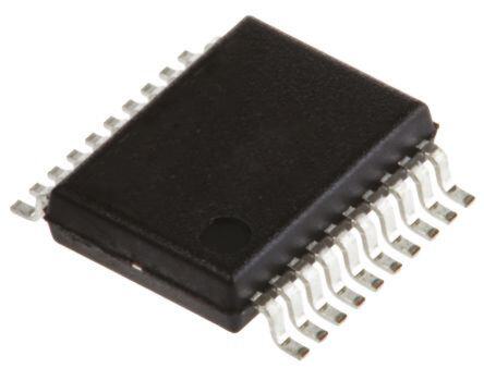
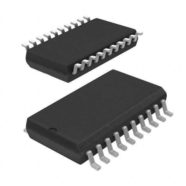
| 描述 | IC ADC 8BIT 100MSPS 3V 20-SSOP模数转换器 - ADC IC 8 BIT 100 MSPS |
| 产品分类 | |
| 品牌 | Analog Devices |
| 产品手册 | |
| 产品图片 |
|
| rohs | 符合RoHS无铅 / 符合限制有害物质指令(RoHS)规范要求 |
| 产品系列 | 数据转换器IC,模数转换器 - ADC,Analog Devices AD9283BRSZ-100- |
| 数据手册 | |
| 产品型号 | AD9283BRSZ-100 |
| 产品目录页面 | |
| 产品种类 | 模数转换器 - ADC |
| 位数 | 8 |
| 供应商器件封装 | 20-SSOP |
| 信噪比 | 47 dB |
| 其它名称 | AD9283BRSZ100 |
| 分辨率 | 8 bit |
| 包装 | 管件 |
| 商标 | Analog Devices |
| 安装类型 | 表面贴装 |
| 安装风格 | SMD/SMT |
| 封装 | Tube |
| 封装/外壳 | 20-SSOP(0.209",5.30mm 宽) |
| 封装/箱体 | SSOP-20 |
| 工作温度 | -40°C ~ 85°C |
| 工作电源电压 | 3.3 V |
| 工厂包装数量 | 66 |
| 接口类型 | Parallel |
| 数据接口 | 并联 |
| 最大功率耗散 | 120 mW |
| 最大工作温度 | + 85 C |
| 最小工作温度 | - 25 C |
| 标准包装 | 66 |
| 特性 | - |
| 电压参考 | Internal, External |
| 电压源 | 单电源 |
| 系列 | AD9283 |
| 结构 | Pipeline |
| 转换器数 | 1 |
| 转换器数量 | 1 |
| 转换速率 | 80 MS/s |
| 输入数和类型 | 2 个单端,单极1 个差分,单极 |
| 输入类型 | Differential |
| 通道数量 | 1 Channel |
| 采样率(每秒) | 100M |


- 商务部:美国ITC正式对集成电路等产品启动337调查
- 曝三星4nm工艺存在良率问题 高通将骁龙8 Gen1或转产台积电
- 太阳诱电将投资9.5亿元在常州建新厂生产MLCC 预计2023年完工
- 英特尔发布欧洲新工厂建设计划 深化IDM 2.0 战略
- 台积电先进制程称霸业界 有大客户加持明年业绩稳了
- 达到5530亿美元!SIA预计今年全球半导体销售额将创下新高
- 英特尔拟将自动驾驶子公司Mobileye上市 估值或超500亿美元
- 三星加码芯片和SET,合并消费电子和移动部门,撤换高东真等 CEO
- 三星电子宣布重大人事变动 还合并消费电子和移动部门
- 海关总署:前11个月进口集成电路产品价值2.52万亿元 增长14.8%


PDF Datasheet 数据手册内容提取
a 8-Bit, 50 MSPS/80 MSPS/100 MSPS 3 V A/D Converter AD9283 FEATURES FUNCTIONAL BLOCK DIAGRAM 8-Bit, 50, 80, and 100 MSPS ADC Low Power: 90 mW at 100 MSPS VD PWRDWN VDD On-Chip Reference and Track/Hold 475 MHz Analog Bandwidth AD9283 SNR = 46.5 dB @ 41 MHz at 100 MSPS 1S iVn gpl-ep 3 A.0n Val oSgu pInpplyu tO Rpaenragteion (2.7 V–3.6 V) AAIINN T/H ADC SOTUATGPIUNTG 8 D7–D0 Power-Down Mode: 4.2 mW ENCODE TIMING REF APPLICATIONS Battery Powered Instruments GND REF REF OUT IN Hand-Held Scopemeters Low Cost Digital Oscilloscopes GENERAL DESCRIPTION The encoder input is TTL/CMOS compatible. A power-down The AD9283 is an 8-bit monolithic sampling analog-to-digital function may be exercised to bring total consumption to converter with an on-chip track-and-hold circuit and is opti- 4.2 mW. In power-down mode, the digital outputs are driven mized for low cost, low power, small size and ease of use. The to a high impedance state. product operates at a 100 MSPS conversion rate, with outstand- Fabricated on an advanced CMOS process, the AD9283 is ing dynamic performance over its full operating range. available in a 20-lead surface mount plastic package (SSOP) The ADC requires only a single 3.0 V (2.7 V to 3.6 V) power specified over the industrial temperature range (–40°C to +85°C). supply and an encode clock for full performance operation. No external reference or driver components are required for many applications. The digital outputs are TTL/CMOS compatible and a separate output power supply pin supports interfacing with 3.3 V or 2.5 V logic. REV.C Information furnished by Analog Devices is believed to be accurate and reliable. However, no responsibility is assumed by Analog Devices for its use, nor for any infringements of patents or other rights of third parties that One Technology Way, P.O. Box 9106, Norwood, MA 02062-9106, U.S.A. may result from its use. No license is granted by implication or otherwise Tel: 781/329-4700 www.analog.com under any patent or patent rights of Analog Devices. Fax: 781/326-8703 © Analog Devices, Inc., 2001
AD9283–SPECIFICATIONS (V = 3.0 V, V = 3.0 V; single-ended input; external reference, unless otherwise noted) DD D Test AD9283BRS-100 AD9283BRS-80 AD9283BRS-50 Parameter Temp Level Min Typ Max Min Typ Max Min Typ Max Unit RESOLUTION 8 8 8 Bits DC ACCURACY Differential Nonlinearity 25°C I ±0.5 +1.25 ±0.5 +1.25 ±0.5 +1.25 LSB Full VI +1.50 +1.50 +1.50 LSB Integral Nonlinearity 25°C I –1.25 ±0.75 +1.25 –1.25 ±0.75 +1.25 –1.25 ±0.75 +1.25 LSB Full VI +2.25 +1.50 +1.50 LSB No Missing Codes Full VI Guaranteed Guaranteed Guaranteed Gain Error1 25°C I –6 ±2.5 +6 –6 ±2.5 +6 –6 ±2.5 +6 % FS Full VI –8 +8 –8 +8 –8 +8 % FS Gain Tempco1 Full VI 80 80 80 ppm/°C ANALOG INPUT Input Voltage Range (With Respect to A ) Full V ±512 ±512 ±512 mV p-p IN Common-Mode Voltage Full V ±200 ±200 ±200 mV Input Offset Voltage 25°C I –35 ±10 +35 –35 ±10 +35 –35 ±10 +35 mV Full VI ±40 ±40 ±40 mV Reference Voltage Full VI 1.2 1.25 1.3 1.2 1.25 1.3 1.2 1.25 1.3 V Reference Tempco Full VI ±130 ±130 ±130 ppm/°C Input Resistance 25°C I 7 10 13 7 10 13 7 10 13 kΩ Full VI 5 16 5 16 5 16 kΩ Input Capacitance 25°C V 2 2 2 pF Full VI µA Analog Bandwidth, Full Power 25°C V 475 475 475 MHz SWITCHING PERFORMANCE Maximum Conversion Rate Full VI 100 80 50 MSPS Minimum Conversion Rate 25°C IV 1 1 1 MSPS Encode Pulsewidth High (t ) 25°C IV 4.3 1000 5.0 1000 8.0 1000 ns EH Encode Pulsewidth Low (t ) 25°C IV 4.3 1000 5.0 1000 8.0 1000 ns EL Aperture Delay (t ) 25°C V 0 0 0 ns A Aperture Uncertainty (Jitter) 25°C V 5 5 5 ps rms Output Valid Time (t )2 Full VI 2.0 3.0 2.0 3.0 2.0 3.0 ns V Output Propagation Delay (t )2 Full VI 4.5 7.0 4.5 7.0 4.5 7.0 ns PD DIGITAL INPUTS Logic “1” Voltage Full VI 2.0 2.0 2.0 V Logic “0” Voltage Full VI 0.8 0.8 0.8 V Logic “1” Current Full VI ±1 ±1 ±1 µA Logic “0” Current Full VI ±1 ±1 ±1 µA Input Capacitance 25°C V 2.0 2.0 2.0 pF DIGITAL OUTPUTS Logic “1” Voltage Full VI 2.95 2.95 2.95 V Logic “0” Voltage Full VI 0.05 0.05 0.05 V Output Coding Offset Binary Code Offset Binary Code Offset Binary Code POWER SUPPLY Power Dissipation3, 4 Full VI 90 120 90 115 80 100 mW Power-Down Dissipation Full VI 4.2 7 4.2 7 4.2 7 mW Power Supply Rejection Ratio (PSRR) 25°C I 18 18 18 mV/V –2– REV. C
AD9283 Test AD9283BRS-100 AD9283BRS-80 AD9283BRS-50 Parameter Temp Level Min Typ Max Min Typ Max Min Typ Max Unit DYNAMIC PERFORMANCE5 Transient Response 25°C V 2 2 2 ns Overvoltage Recovery Time 25°C V 2 2 2 ns Signal-to-Noise Ratio (SNR) (Without Harmonics) f = 10.3 MHz 25°C I 46.5 47 44 47 dB IN f = 27 MHz 25°C I 46.5 44 47 47 dB IN f = 41 MHz 25°C I 43.5 46.5 47 dB IN f = 76 MHz 25°C V 46.0 dB IN Signal-to-Noise Ratio (SINAD) (With Harmonics) f = 10.3 MHz 25°C I 45 47 43.5 46.5 dB IN f = 27 MHz 25°C I 45.5 43.5 46.5 46 dB IN f = 41 MHz 25°C I 42.5 45 42 dB IN f = 76 MHz 25°C V 42.5 dB IN Effective Number of Bits f = 10.3 MHz 25°C I 7.3 7.5 7.6 Bits IN f = 27 MHz 25°C I 7.4 7.5 7.5 Bits IN f = 41 MHz 25°C I 7.3 7.5 Bits IN f = 76 MHz 25°C V 6.9 Bits IN 2nd Harmonic Distortion f = 10.3 MHz 25°C I 57 60 55 60 dBc IN f = 27 MHz 25°C I 60 55 60 56 dBc IN f = 41 MHz 25°C I 50 58 55 dBc IN f = 76 MHz 25°C V 46 dBc IN 3rd Harmonic Distortion f = 10.3 MHz 25°C I 54.5 70 55 70 dBc IN f = 27 MHz 25°C I 55 55 62.5 60 dBc IN f = 41 MHz 25°C I 47 52.5 60 dBc IN f = 76 MHz 25°C V 53 dBc IN Two-Tone Intermod Distortion (IMD) f = 10.3 MHz 25°C V 52 52 52 dBc IN NOTES 1Gain error and gain temperature coefficient are based on the ADC only (with a fixed 1.25 V external reference). 2t and t are measured from the 1.5 V level of the ENCODE input to the 50%/50% levels of the digital outputs swing. The digital output load during test is not to V PD exceed an ac load of 10 pF or a dc current of ±40 µA. 3Power dissipation measured with encode at rated speed and a dc analog input. 4Typical thermal impedance for the RS style (SSOP) 20-lead package: θ = 46°C/W, θ = 80°C/W, θ = 126°C/W. JC CA JA 5SNR/harmonics based on an analog input voltage of –0.7 dBFS referenced to a 1.024 V full-scale input range. Specifications subject to change without notice. *Stresses above those listed under Absolute Maximum Ratings may cause perma- ABSOLUTE MAXIMUM RATINGS* nent damage to the device. This is a stress rating only; functional operation of the VD, VDD . . . . . . . . . . . . . . . . . . . . . . . . . . . . . . . . . . . . . . . 4 V device at these or any other conditions outside of those indicated in the operation Analog Inputs . . . . . . . . . . . . . . . . . . . . –0.5 V to V + 0.5 V sections of this specification is not implied. Exposure to absolute maximum ratings D Digital Inputs . . . . . . . . . . . . . . . . . . . –0.5 V to V + 0.5 V for extended periods may affect device reliability. DD VREF IN . . . . . . . . . . . . . . . . . . . . . . . . –0.5 V to V + 0.5 V D Digital Output Current . . . . . . . . . . . . . . . . . . . . . . . . 20 mA ORDERING GUIDE Operating Temperature . . . . . . . . . . . . . . . . –55°C to +125°C Storage Temperature . . . . . . . . . . . . . . . . . . –65°C to +150°C Temperature Package Package Maximum Junction Temperature . . . . . . . . . . . . . . . . 150°C Model Ranges Descriptions Options Maximum Case Temperature . . . . . . . . . . . . . . . . . . . 150°C AD9283BRS -50, -80, -100 –40°C to +85°C 20-Lead SSOP RS-20 AD9283/PCB 25°C Evaluation Board CAUTION ESD (electrostatic discharge) sensitive device. Electrostatic charges as high as 4000V readily WARNING! accumulate on the human body and test equipment and can discharge without detection. Although the AD9283 features proprietary ESD protection circuitry, permanent damage may occur on devices subjected to high-energy electrostatic discharges. Therefore, proper ESD ESD SENSITIVE DEVICE precautions are recommended to avoid performance degradation or loss of functionality. REV. C –3–
AD9283 EXPLANATION OF TEST LEVELS Table I. Output Coding (VREF = 1.25 V) Test Level I 100% production tested. Step AIN–AIN Digital Output II 100% production tested at 25°C and sample tested at 255 0.512 11111111 specified temperatures. • • • III Sample tested only. • • • IV Parameter is guaranteed by design and characteriza- 128 0.002 10000000 tion testing. 127 –0.002 01111111 • • • V Parameter is a typical value only. • • • VI 100% production tested at 25°C; guaranteed by design and 0 –0.512 00000000 characterization testing for industrial temperature range; 100% production tested at temperature extremes for mili- tary devices. PIN CONFIGURATION PWRDWN 1 20 D0 (LSB) VREF OUT 2 19 D1 VREF IN 3 18 D2 GND 4 17 D3 VD 5 AD9283 16 GND AIN 6 (NToOt Pto V SIEcaWle)15 VDD AIN 7 14 D4 VD 8 13 D5 GND 9 12 D6 ENCODE 10 11 D7 (MSB) PIN FUNCTION DESCRIPTIONS Pin Number Mnemonic Function 1 PWRDWN Power-Down Function Select; Logic HIGH for Power-Down Mode (Digital Outputs Go to High Impedance State) 2 VREF OUT Internal Reference Output (1.25 V typ); Bypass with 0.1 µF to Ground 3 VREF IN Reference Input for ADC (1.25 V typ) 4, 9, 16 GND Ground 5, 8 V Analog 3 V Power Supply D 6 A Analog Input for ADC (Can Be Left Open if Operating in Single-Ended Mode, but Rec- IN ommend Connection to a 0.1 µF Capacitor and a 25 Ω Resistor in Series to Ground for Better Input Matching) 7 A Analog Input for ADC IN 10 ENCODE Encode Clock for ADC (ADC Samples on Rising Edge of ENCODE) 11–14, 17–20 D7–D4, D3–D0 Digital Outputs of ADC 15 V Digital output power supply. Nominally 2.5 V to 3.6 V DD –4– REV. C
AD9283 SAMPLE N SAMPLE N+1 SAMPLE N+4 SAMPLE N+5 AIN tA SAMPLE N+2 SAMPLE N+3 tEH tEL 1/fS ENCODE tPD tV D7–D0 DATA N–4 DATA N–3 DATA N–2 DATA N–1 DATA N DATA N+1 Figure 1.Timing Diagram VDD VDD 33.3k(cid:1) 33.3k(cid:1) OUT AIN AIN 14.3k(cid:1) 14.3k(cid:1) Figure 2.Equivalent Analog Input Circuit Figure 5.Equivalent Digital Output Circuit VD VD VBIAS REF IN OUT Figure 3.Equivalent Reference Input Circuit Figure 6.Equivalent Reference Output Circuit VD ENCODE Figure 4. Equivalent Encode Input Circuit REV. C –5–
AD9283– Typical Performance Characteristics 70 0 2ND ENCODE = 100MSPS –10 ENCODE = 100MSPS 65 AIN = 10.3MHz –20 SNR = 46.5dB 60 SINAD = 45dB –30 2nd = 57dBc 3RD 55 3rd = 54.5dBc –40 B50 dB–50 d 45 –60 –70 40 –80 35 –90 30 –100 10 20 30 40 50 60 80 100 FREQUENCY FREQUENCY – AIN TPC 1.Spectrum: f = 100 MSPS, f = 10.3 MHz TPC 4.Harmonic Distortion vs. A Frequency S IN IN 0 0 ENCODE = 100MSPS ENCODE = 100MSPS –10 –10 AIN = 41MHz AIN1 = 9MHz –20 SSINNRA D= 4=6 4.55ddBB –20 IAMIND2 = = 5 120dMBHcz 2nd = 58dBc –30 3rd = 52.5dBc –30 –40 –40 B B d d –50 –50 –60 –60 –70 –70 –80 –80 –90 –90 FREQUENCY FREQUENCY TPC 2.Spectrum: f = 100 MSPS, f = 40 MHz TPC 5.Two-Tone Intermodulation Distortion S IN 0 55 –10 ENCODE = 100MSPS ENCODE = 100MSPS AIN = 76MHz –20 SNR = 46dB 50 SINAD = 42.5dB 2nd = 46dBc SNR –30 3rd = 53dBc 45 –40 dB dB –50 SINAD 40 –60 –70 35 –80 –90 30 FREQUENCY 10 20 30 40 50 60 80 90 100 FREQUENCY TPC 3.Spectrum: f = 100 MSPS, f = 76 MHz TPC 6.SINAD/SNR vs. A Frequency S IN IN –6– REV. C
AD9283 49 120 SNR AIN = 10.3MHz AIN = 10.3MHz 48 100 SINAD 47 80 W m – dB46 ER 60 W O P 45 40 44 20 43 0 10 20 30 40 50 60 70 80 90 100 10 20 30 40 50 60 70 80 90 100 ENCODE RATE ENCODE RATE TPC 7.SINAD/SNR vs. Encode Rate TPC 10.Analog Power Dissipation vs. Encode Rate 60 49 ENCODE = 100MSPS AIN = 10.3MHz 50 48 SNR 40 SNR SINAD 47 dB30 dB SINAD 46 20 45 10 0 44 7.0 6.5 6.0 5.5 5.0 4.5 4.0 3.5 3.0 –60 –40 –20 0 20 40 60 80 100 ENCODE PULSEWIDTH HIGH – ns TEMPERATURE – (cid:1)C TPC 8.SINAD/SNR vs. Encode Pulsewidth High TPC 11.SINAD/SNR vs. Temperature 0.5 1.00 0.0 0.75 –0.5 –1.0 0.50 –1.5 0.25 –2.0 dB–2.5 LSB 0.00 –3.0 –0.25 –3.5 –4.0 –0.50 –4.5 –0.75 –5.0 –5.5 –1.00 0 100 200 300 400 500 600 CODE BANDWIDTH – MHz TPC 9.ADC Frequency Response: f = 100 MSPS TPC 12.Differential Nonlinearity S REV. C –7–
AD9283 Digital Outputs 2.0 The digital outputs are TTL/CMOS compatible. The output 1.5 buffers are powered from a separate supply, allowing adjustment of the output voltage swing to ease interfacing with 2.5 V or 1.0 3.3 V logic. The AD9283 goes into a low power state within two clock cycles following the assertion of the PWRDWN input. 0.5 PWRDWN is asserted with a logic high. During power-down SB 0.0 the outputs transition to a high impedance state. The time it L takes to achieve optimal performance after disabling the power- –0.5 down mode is approximately 15 clock cycles. Care should be taken when loading the digital outputs of any high speed ADC. –1.0 Large output loads create current transients on the chip that can –1.5 degrade the converter’s performance. –2.0 Voltage Reference CODE A stable and accurate 1.25 V voltage reference is built into the AD9283 (VREF OUT). In normal operation, the internal refer- TPC 13.Integral Nonlinearity ence is used by strapping Pins 2 and 3 of the AD9283 together. The input range can be adjusted by varying the reference volt- APPLICATIONS age applied to the AD9283. No degradation in performance Theory of Operation occurs when the reference is adjusted ±5%. The full-scale range The analog signal is applied differentially or single-endedly to of the ADC tracks reference voltage changes linearly. Whether the inputs of the AD9283. The signal is buffered and fed for- used or not, the internal reference (Pin 2) should be bypassed ward to an on-chip sample-and-hold circuit. The ADC core with a 0.1 µF capacitor to ground. architecture is a bit-per-stage pipeline type converter utilizing switch capacitor techniques. The bit-per-stage blocks determine Timing the 5 MSBs and drive a FLASH converter to encode the 3 LSBs. The AD9283 provides latched data outputs with four pipeline Each of the 5 MSB stages provides sufficient overlap and error delays. Data outputs are available one propagation delay (tPD) correction to allow optimization of performance with respect to after the rising edge of the encode command (Figure 1. Timing comparator accuracy. The output staging block aligns the data, Diagram). The minimum guaranteed conversion rate to the carries out the error correction and feeds the data to the eight ADC is 1 MSPS. The dynamic performance of the converter output buffers. The AD9283 includes an on-chip reference will degrade at encode rates below this sample rate. (nominally 1.25 V) and generates all clocking signals from one Evaluation Board externally applied encode command. This makes the ADC easy The AD9283 evaluation board offers an easy way to test the to interface with and requires very few external components for AD9283. It only requires a 3 V supply, an analog input and operation. encode clock to test the AD9283. The board is shipped with the ENCODE Input 100 MSPS grade ADC. The ENCODE input is fully TTL/CMOS compatible with a The analog input to the board accepts a 1 V p-p signal centered nominal threshold of 1.5 V. Care was taken on the chip to at ground. J1 should be used (Jump E3–E4, E18–E19) to drive match clock line delays and maintain sharp clock logic transi- the ADC through Transformer T1. J2 should be used for single- tions. Any high speed A/D converter is extremely sensitive to ended input drive (Jump E19–E21). the quality of the sampling clock provided by the user. This Both J1 and J2 are terminated to 50 Ω on the PCB. Each analog ADC uses an on-chip sample-and-hold circuit which is essen- path is ac-coupled to an on-chip resistor divider which provides tially a mixer. Any timing jitter on the ENCODE will be com- the required dc bias. bined with the desired signal and degrade the high frequency performance of the ADC. The user is advised to give commen- A (TTL/CMOS Level) sample clock is applied to connector surate thought to the clock source. J3 which is terminated through 50 Ω on the PCB. This clock is buffered by U5 which also provides the clocks for the 574 Analog Input latches, DAC, and the off-card latch clock CLKCON. (Timing The analog input to the ADC is fully differential and both inputs can be modified at E17.) are internally biased. This allows the most flexible use of ac or dc and differential or single-ended input modes. For peak performance There is a reconstruction DAC (AD9760) on the PCB. The the inputs are biased at 0.3 × V . See the specification table for DAC is on the board to assist in debug only—the outputs D allowable common-mode range when dc coupling the input. should not be used to measure performance of the ADC. The inputs are also buffered to reduce the load the user needs to drive. For best dynamic performance, the impedances at A and IN A should be matched. The importance of this increases with IN sampling rate and analog input frequency. The nominal input range is 1.024 V p-p. –8– REV. C
AD9283 Figure 7.Printed Circuit Board Top Side Silkscreen Figure 9.Printed Circuit Board Top Side Copper Figure 8.Printed Circuit Board Bottom Side Silkscreen Figure 10.Printed Circuit Board “Split” Power Layer REV. C –9–
AD9283 Figure 11.Printed Circuit Board Ground Layer Figure 12.Printed Circuit Board Bottom Side Copper EVALUATION BOARD BILL OF MATERIALS — GS01717 # Qty REFDES Device Package Value 1 15 C1, C4–C17 Ceramic Cap 0603 0.1 µF 2 4 C18–C21 Tantalum Cap BCAPTAJD 10 µF 3 24 E1–E6, E8–E10, E12–E19, E21, E34–E39 W-HOLE 4 4 J1, J2, J3, J5 Connector SMB 5 1 P1 5-Pin Connector Wieland Connector (P/N #25.602.2553.0 Top P/N #Z5.530.0525.0 Bottom) 6 1 P2 37-Pin Connector AMP-747462-2 7 5 R4, R9, R10, R21, R22 Resistor 1206 50 Ω 8 1 R7 Resistor 1206 25 Ω 9 1 R23 Resistor 1206 2 kΩ 10 1 T1 Transformer Mini-Circuits T1-1T-KK81 11 1 U1 AD9283 SSOP-20 12 1 U3 AD9760 SOIC-28 13 1 U4 74ACQ574 SOIC-20 14 1 U5 SN74LVC86 SO14 –10– REV. C
AD9283 F P P27DR 3 1234567890123456789012345678901234567 C 1111111111222222222233333333 N O C K L C 5 J 0 1 2 3 4 5 6 7 A A A A A A A A VDLD D D D D D D D CLKLAT VDAC R21(cid:1)50 C16(cid:3)0.1F C11(cid:3)0.1F R22(cid:1)50 C 20C19018117216315414513612711K E38 E39 VDA R23(cid:1)2k VDAC C21(cid:3)F10F U4CQ574 VC Q Q Q Q Q Q Q Q CLOC E36 E37 C10(cid:3)0.1F C VDAC C12(cid:3)0.1F VDL C20(cid:3)F10 74A OUT_EN D0 D1 D2 D3 D4 D5 D6 D7 GND CLKDA C15(cid:3)0.1F C14(cid:3)0.1F 9(cid:3) 4 5 D C110 1 2 3 4 5 6 7 8 9 10 E3 E3 2827262524232221201918171615 V VA C18(cid:3)10F 60 CLKDVDDDCOMNC5AVDDCOMP2IOUTAIOUTBACOMCOMP1FSADJREFIOREFLOSLEEP U3D97 A D V 98765432101234 BBBBBBBBBBCCCC F DDDDDDDDDDNNNN 9(cid:3) C0.1 1234567891011121314 20 19 18 17 16 15 14 13 12 11 A7A6A5A4A3A2A1A0 0 1 2 3 D D 4 5 6 7 DDDDDDDD D D D D N D D D D D 3 G V 8 PWDNU1AD92 1PWDN E22REFOUT 3REFIN 4GND 5VA 6AIN 7AIN 8VA1 9GND 10C C13(cid:3)0.1F VDL E13E14VDLE12 E8 E5 E1 VA EN LAT DAC E9 E10 E6 C5(cid:3)0.1F C4(cid:3)0.1F CLK CLK A 1413 121110 98 V CB AYB AY C1(cid:3)0.1F C8(cid:3)0.1F (cid:3)FR7(cid:1)25(cid:3)F U5SN74LVC86 1AVC1B4 41Y2A42B3 2Y3GND3 5 LVDAC VAC60.1 C70.1 C17(cid:3)0.1F 12 3ENC45KCON67 4 D L P1 23 VDGNDV T143 52 61 E18 E19E21 R9(cid:1)50 E17E15LCE16 D 1 VA E4 2 0(cid:1) V E3 R4(cid:1)50 J R150 3 1 J J Figure 13.Printed Circuit Board Schematic REV. C –11–
AD9283 OUTLINE DIMENSIONS Dimensions shown in inches and (mm). 20-Lead Shrink Small Outline Package (SSOP) (RS-20) C) 1( 0 0/ 0.295 (7.50) 1 – 0.271 (6.90) 0 – b 4 8 20 11 05 0 0.311 (7.9)0.301 (7.64) 1 10 0.212 (5.38)0.205 (5.21) C 0.078 (1.98)PIN 1 0.07 (1.78) 0.068 (1.73) 0.066 (1.67) 8° 0.037 (0.94) 0.008 (0.203) 0(.00.26556) SEATING 0.009 (0.229) 0° 0.022 (0.559) 0.002 (0.050) BSC PLANE 0.005 (0.127) Revision History Location Page Data Sheet changed from REV. B to REV. C. Edits to ABSOLUTE MAXIMUM RATINGS . . . . . . . . . . . . . . . . . . . . . . . . . . . . . . . . . . . . . . . . . . . . . . . . . . . . . . . . . . . . . . . . . 3 A. S. U. N D I E T N RI P –12– REV. C