ICGOO在线商城 > 集成电路(IC) > 数据采集 - 模数转换器 > ADS1255IDBR
 Datasheet下载
- 型号: ADS1255IDBR
- 制造商: Texas Instruments
- 库位|库存: xxxx|xxxx
- 要求:
| 数量阶梯 | 香港交货 | 国内含税 |
| +xxxx | $xxxx | ¥xxxx |
查看当月历史价格
查看今年历史价格
ADS1255IDBR产品简介:
ICGOO电子元器件商城为您提供ADS1255IDBR由Texas Instruments设计生产,在icgoo商城现货销售,并且可以通过原厂、代理商等渠道进行代购。 ADS1255IDBR价格参考。Texas InstrumentsADS1255IDBR封装/规格:数据采集 - 模数转换器, 24 Bit Analog to Digital Converter 1, 2 Input 1 Sigma-Delta 20-SSOP。您可以下载ADS1255IDBR参考资料、Datasheet数据手册功能说明书,资料中有ADS1255IDBR 详细功能的应用电路图电压和使用方法及教程。
Texas Instruments(德州仪器)的ADS1255IDBR是一款高精度、低功耗的24位模数转换器(ADC),适用于多种应用场景。以下是其主要应用领域:

 1. 工业自动化与控制
   ADS1255IDBR在工业自动化中用于精确测量传感器数据,如温度、压力、位移等。它能够提供高分辨率的数据采集,确保控制系统对环境变化的响应更加精准和稳定。例如,在精密制造过程中,该ADC可以用于监测设备的工作状态,确保生产过程中的每一个参数都处于最佳范围内。

 2. 医疗设备
   在医疗设备中,ADS1255IDBR可用于心电图(ECG)、血压计、血糖仪等设备中,以实现对生物电信号的高精度采集。其低噪声和高分辨率特性,使得它可以准确捕捉微弱的生理信号,帮助医生做出更准确的诊断。

 3. 能源管理
   ADS1255IDBR在智能电网、太阳能逆变器等能源管理系统中发挥重要作用。它可以实时监测电力系统的电压、电流等参数,帮助优化能源分配,提高能源利用效率。此外,它还可以用于电池管理系统(BMS),精确监控电池的充电和放电状态,延长电池寿命。

 4. 环境监测
   环境监测设备需要长时间、高精度地采集各种环境参数,如空气质量、水质、土壤湿度等。ADS1255IDBR凭借其出色的线性度和稳定性,能够为这些应用提供可靠的数据支持。特别是在野外或恶劣环境下,它的低功耗特性有助于延长设备的运行时间。

 5. 农业与物联网
   在智慧农业和物联网(IoT)应用中,ADS1255IDBR可用于监测土壤湿度、光照强度、温湿度等环境参数。通过将这些数据传输到云端,农民可以根据实时数据调整灌溉、施肥等操作,实现精细化管理,提高农作物产量。

总之,ADS1255IDBR凭借其高精度、低功耗和广泛的工作温度范围,适用于多种高要求的应用场景,尤其是在需要精确数据采集和处理的场合中表现出色。
| 参数 | 数值 |
| 产品目录 | 集成电路 (IC)半导体 |
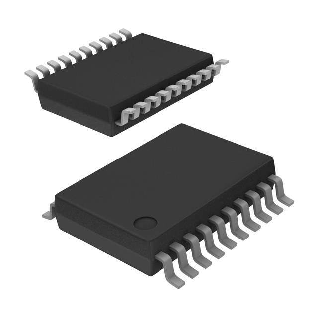
| 描述 | IC ADC 24-BIT SPI PROGBL 20-SSOP模数转换器 - ADC 24 Bit 30kSPS Very Lo-Noise Delta-Sigma |
| 产品分类 | |
| 品牌 | Texas Instruments |
| 产品手册 | |
| 产品图片 |
|
| rohs | 符合RoHS无铅 / 符合限制有害物质指令(RoHS)规范要求 |
| 产品系列 | 数据转换器IC,模数转换器 - ADC,Texas Instruments ADS1255IDBR- |
| 数据手册 | |
| 产品型号 | ADS1255IDBR |
| 产品培训模块 | http://www.digikey.cn/PTM/IndividualPTM.page?site=cn&lang=zhs&ptm=13240 |
| 产品目录页面 | |
| 产品种类 | 模数转换器 - ADC |
| 位数 | 24 |
| 供应商器件封装 | 20-SSOP |
| 信噪比 | Yes |
| 其它名称 | 296-25897-6 |
| 分辨率 | 24 bit |
| 制造商产品页 | http://www.ti.com/general/docs/suppproductinfo.tsp?distId=10&orderablePartNumber=ADS1255IDBR |
| 包装 | 剪切带 (CT) |
| 单位重量 | 156.700 mg |
| 商标 | Texas Instruments |
| 安装类型 | 表面贴装 |
| 安装风格 | SMD/SMT |
| 封装 | Reel |
| 封装/外壳 | 20-SSOP(0.209",5.30mm 宽) |
| 封装/箱体 | SSOP-20 |
| 工作温度 | -40°C ~ 105°C |
| 工作电源电压 | 1.8 V to 3.6 V, 4.75 V to 5.25 V |
| 工厂包装数量 | 1000 |
| 接口类型 | 2-Wire, Microwire, QSPI, Serial, SPI |
| 数据接口 | SPI |
| 最大功率耗散 | 57 mW |
| 最大工作温度 | + 85 C |
| 最小工作温度 | - 40 C |
| 标准包装 | 1 |
| 特性 | PGA |
| 电压参考 | External |
| 电压源 | 模拟和数字 |
| 系列 | ADS1255 |
| 结构 | Sigma-Delta |
| 视频文件 | http://www.digikey.cn/classic/video.aspx?PlayerID=1364138032001&width=640&height=455&videoID=44659313001 |
| 转换器数 | 1 |
| 转换器数量 | 1 |
| 转换速率 | 30 kS/s |
| 输入数和类型 | 2 个单端,单极1 个差分,单极 |
| 输入类型 | Single-Ended |
| 通道数量 | 2 Channel |
| 采样率(每秒) | 2.5k ~ 30k |


- 商务部:美国ITC正式对集成电路等产品启动337调查
- 曝三星4nm工艺存在良率问题 高通将骁龙8 Gen1或转产台积电
- 太阳诱电将投资9.5亿元在常州建新厂生产MLCC 预计2023年完工
- 英特尔发布欧洲新工厂建设计划 深化IDM 2.0 战略
- 台积电先进制程称霸业界 有大客户加持明年业绩稳了
- 达到5530亿美元!SIA预计今年全球半导体销售额将创下新高
- 英特尔拟将自动驾驶子公司Mobileye上市 估值或超500亿美元
- 三星加码芯片和SET,合并消费电子和移动部门,撤换高东真等 CEO
- 三星电子宣布重大人事变动 还合并消费电子和移动部门
- 海关总署:前11个月进口集成电路产品价值2.52万亿元 增长14.8%


PDF Datasheet 数据手册内容提取
ADS1255 ADS1256 SBAS288K − JUNE 2003 − REVISED SEPTEMBER 2013 Very Low Noise, 24-Bit Analog-to-Digital Converter FEATURES DESCRIPTION (cid:2) 24 Bits, No Missing Codes The ADS1255 and ADS1256 are extremely low-noise, 24-bit analog-to-digital (A/D) converters. They provide − All Data Rates and PGA Settings (cid:2) complete high-resolution measurement solutions for the Up to 23 Bits Noise-Free Resolution most demanding applications. (cid:2) ±0.0010% Nonlinearity (max) The converter is comprised of a 4th-order, delta-sigma (cid:2) Data Output Rates to 30kSPS (ΔΣ) modulator followed by a programmable digital filter. A (cid:2) Fast Channel Cycling flexible input multiplexer handles differential or − 18.6 Bits Noise-Free (21.3 Effective Bits) single-ended signals and includes circuitry to verify the at 1.45kHz integrity of the external sensor connected to the inputs. (cid:2) The selectable input buffer greatly increases the input One-Shot Conversions with Single-Cycle impedance and the low-noise programmable gain Settling amplifier (PGA) provides gains from 1 to 64 in binary steps. (cid:2) Flexible Input Multiplexer with Sensor Detect The programmable filter allows the user to optimize − Four Differential Inputs (ADS1256 only) between a resolution of up to 23 bits noise-free and a data − Eight Single-Ended Inputs (ADS1256 only) rate of up to 30k samples per second (SPS). The (cid:2) converters offer fast channel cycling for measuring Chopper-Stabilized Input Buffer (cid:2) multiplexed inputs and can also perform one-shot Low-Noise PGA: 27nV Input-Referred Noise conversions that settle in just a single cycle. (cid:2) Self and System Calibration for All PGA Communication is handled over an SPI-compatible serial Settings interface that can operate with a 2-wire connection. (cid:2) 5V Tolerant SPI™-Compatible Serial Interface Onboard calibration supports both self and system (cid:2) Analog Supply: 5V correction of offset and gain errors for all the PGA settings. (cid:2) Bidirectional digital I/Os and a programmable clock output Digital Supply: 1.8V to 3.6V driver are provided for general use. The ADS1255 is (cid:2) Power Dissipation packaged in an SSOP-20, and the ADS1256 in an − As Low as 38mW in Normal Mode SSOP-28. − 0.4mW in Standby Mode AVDD VREFP VREFN DVDD APPLICATIONS (cid:2) AIN0 Clock XTAL1/CLKIN Scientific Instrumentation AIN1 Generator XTAL2 (cid:2) Industrial Process Control AIN2 Mux 1:64 (cid:2) (cid:2) MTeesdt icaanld E Mqeuaipsmureenmtent 56OnlyAAIINN34 SDeaenntesdcotr Buffer PGA 4Mtho−duOlardtoerr PrDoiggritaamlFmilatebrle Control RSYENSCET/PDWN (cid:2) Weigh Scales S12AIN5 DRDY DAIN6 A SCLK AIN7 General Serial Purpose Interface DIN AINCOM DigitalI/O DOUT CS AGND D3 D2 D1 D0/CLKOUT DGND ADS1256 Only Please be aware that an important notice concerning availability, standard warranty, and use in critical applications of TexasInstruments semiconductor products and disclaimers thereto appears at the end of this data sheet. SPI is a trademark of Motorola, Inc. All other trademarks are the property of their respective owners. PRODUCTION DATA information is current as of publication date. Products Copyright © 2003−2013, Texas Instruments Incorporated conform to specifications per the terms of Texas Instruments standard warranty. Production processing does not necessarily include testing of all parameters. www.ti.com
ADS1255 ADS1256 www.ti.com SBAS288K − JUNE 2003 − REVISED SEPTEMBER 2013 ORDERING INFORMATION For the most current package and ordering information, see the Package Option Addendum at the end of this document, or see the TI web site at www.ti.com. This integrated circuit can be damaged by ESD. Texas ABSOLUTE MAXIMUM RATINGS Instruments recommends that all integrated circuits be over operating free-air temperature range unless otherwise noted(1) handled with appropriate precautions. Failure to observe ADS1255, ADS1256 UNIT proper handling and installation procedures can cause damage. AVDD to AGND −0.3 to +6 V ESD damage can range from subtle performance degradation to DVDD to DGND −0.3 to +3.6 V complete device failure. Precision integrated circuits may be more susceptible to damage because very small parametric changes could AGND to DGND −0.3 to +0.3 V cause the device not to meet its published specifications. 100, Momentary mA IInnppuutt CCuurrrreenntt 10, Continuous mA Analog inputs to AGND −0.3 to AVDD + 0.3 V DIN, SCLK, CS, RESET, SYNC/PDWN, −0.3 to +6 V Digital XTAL1/CLKIN to DGND iinnppuuttss D0/CLKOUT, D1, D2, D3 −0.3 to DVDD + 0.3 V to DGND Maximum Junction Temperature +150 °C Operating Temperature Range −40 to +105 °C Storage Temperature Range −60 to +150 °C Lead Temperature (soldering, 10s) +300 °C (1) Stresses above those listed under Absolute Maximum Ratings may cause permanent damage to the device. Exposure to absolute maximum conditions for extended periods may degrade device reliability. These are stress ratings only, and functional operation of the device at these or any other conditions beyond those specified is not implied. 2
ADS1255 ADS1256 www.ti.com SBAS288K − JUNE 2003 − REVISED SEPTEMBER 2013 ELECTRICAL CHARACTERISTICS All specifications at −40°C to +85°C, AVDD = +5V, DVDD = +1.8V, fCLKIN = 7.68MHz, PGA = 1, and VREF = +2.5V, unless otherwise noted. PARAMETER TEST CONDITIONS MIN TYP MAX UNIT Analog Inputs Full-scale input voltage (AINP − AINN) ±2VREF/PGA V AAbbssoolluuttee iinnppuutt vvoollttaaggee Buffer off AGND − 0.1 AVDD + 0.1 V (AIN0-7, AINCOM to AGND) Buffer on AGND AVDD − 2.0 V Programmable gain amplifier 1 64 Buffer off, PGA = 1, 2, 4, 8, 16 150/PGA kΩ Differential inpput imppedance Buffer off, PGA = 32, 64 4.7 kΩ Buffer on, fDATA ≤ 50Hz(1) 80 MΩ SDCS[1:0] = 01 0.5 μA Sensor detect current sources SDCS[1:0] = 10 2 μA SDCS[1:0] = 11 10 μA System Performance Resolution 24 Bit No missing codes All data rates and PGA settings 24 Bit Data rate (fDATA) fCLKIN = 7.68MHz 2.5 30,000 SPS(2) Differential input, PGA = 1 ±0.0003 ±0.0010 %FSR(3) IInntteeggrraall nnoonnlliinneeaarriittyy Differential input, PGA = 64 ±0.0007 %FSR Offset error After calibration On the level of the noise PGA = 1 ±100 nV/°C OOffffsseett ddrriifftt PGA = 64 ±4 nV/°C After calibration, PGA = 1, Buffer on ±0.005 % GGaaiinn eerrrroorr After calibration, PGA = 64, Buffer on ±0.03 % PGA = 1 ±0.8 ppm/°C GGaaiinn ddrriifftt PGA = 64 ±0.8 ppm/°C Common-mode rejection fCM(4) = 60Hz, fDATA = 30kSPS(5) 95 110 dB Noise See Noise Performance Tables AVDD power-supply rejection ±5% Δ in AVDD 60 70 dB DVDD power-supply rejection ±10% Δ in DVDD 100 dB Voltage Reference Inputs Reference input voltage (VREF) VREF ≡ VREFP − VREFN 0.5 2.5 2.6 V Buffer off AGND − 0.1 VREFP − 0.5 V NNeeggaattiivvee rreeffeerreennccee iinnppuutt ((VVRREEFFNN)) Buffer on(6) AGND VREFP − 0.5 V Buffer off VREFN + 0.5 AVDD + 0.1 V PPoossiittiivvee rreeffeerreennccee iinnppuutt ((VVRREEFFPP)) Buffer on(6) VREFN + 0.5 AVDD − 2.0 V Voltage reference impedance fCLKIN = 7.68MHz 18.5 kΩ Digital Input/Output DIN, SCLK, XTAL1/CLKIN, 0.8 DVDD 5.25 V VVIIHH SYNC/PDWN, CS, RESET D0/CLKOUT, D1, D2, D3 0.8 DVDD DVDD V VIL DGND 0.2 DVDD V VOH IOH = 5mA 0.8 DVDD V VOL IOL = 5mA 0.2 DVDD V Input hysteresis 0.5 V Input leakage 0 < VDIGITAL INPUT < DVDD ±10 μA External crystal between XTAL1 and 2 7.68 10 MHz MMaasstteerr cclloocckk rraattee XTAL2 External oscillator driving CLKIN 0.1 7.68 10 MHz 3
ADS1255 ADS1256 www.ti.com SBAS288K − JUNE 2003 − REVISED SEPTEMBER 2013 ELECTRICAL CHARACTERISTICS (continued) All specifications at −40°C to +85°C, AVDD = +5V, DVDD = +1.8V, fCLKIN = 7.68MHz, PGA = 1, and VREF = +2.5V, unless otherwise noted. PARAMETER TEST CONDITIONS MIN TYP MAX UNIT Power-Supply AVDD 4.75 5.25 V DVDD 1.8 3.6 V Power-down mode 2 μA Standby mode 20 μA Normal mode, PGA = 1, Buffer off 7 10 mA AAVVDDDD ccuurrrreenntt Normal mode, PGA = 64, Buffer off 16 22 mA Normal mode, PGA = 1, Buffer on 13 19 mA Normal mode, PGA = 64, Buffer on 36 50 mA Power-down mode 2 μA Standby mode, CLKOUT off, 95 μA DVDD current DVDD = 3.3V Normal mode, CLKOUT off, 0.9 2 mA DVDD = 3.3V Normal mode, PGA = 1, Buffer off, 38 57 mW PPoowweerr ddiissssiippaattiioonn DVDD = 3.3V Standby mode, DVDD = 3.3V 0.4 mW Temperature Range Specified −40 +85 °C Operating −40 +105 °C Storage −60 +150 °C (1) See text for more information on input impedance. (2) SPS = samples per second. (3) FSR = full-scale range = 4VREF/PGA. (4) fCM is the frequency of the common-mode input signal. (5) Placing a notch of the digital filter at 60Hz (setting fDATA = 60SPS, 30SPS, 15SPS, 10SPS, 5SPS, or 2.5SPS) will further improve the common-mode rejection of this frequency. (6) The reference input range with Buffer on is restricted only if self-calibration or gain self-calibration is to be used. If using system calibration or writing calibration values directly to the registers, the entire Buffer off range can be used. 4
ADS1255 ADS1256 www.ti.com SBAS288K − JUNE 2003 − REVISED SEPTEMBER 2013 PIN ASSIGNMENTS SSOP PACKAGE AVDD 1 28 D3 (TOP VIEW) AGND 2 27 D2 AVDD 1 20 D1 VREFN 3 26 D1 AGND 2 19 D0/CLKOUT VREFP 4 25 D0/CLKOUT VREFN 3 18 SCLK AINCOM 5 24 SCLK VREFP 4 17 DIN AIN0 6 23 DIN AINCOM 5 16 DOUT AIN1 7 22 DOUT ADS1255 ADS1256 AIN0 6 15 DRDY AIN2 8 21 DRDY AIN1 7 14 CS AIN3 9 20 CS SYNC, PDWN 8 13 XTAL1/CLKIN AIN4 10 19 XTAL1/CLKIN RESET 9 12 XTAL2 AIN5 11 18 XTAL2 DVDD 10 11 DGND AIN6 12 17 DGND AIN7 13 16 DVDD SYNC, PDWN 14 15 RESET Terminal Functions TERMINAL NO. AANNAALLOOGG//DDIIGGIITTAALL NAME ADS1255 ADS1256 INPUT/OUTPUT DESCRIPTION AVDD 1 1 Analog Analog power supply AGND 2 2 Analog Analog ground VREFN 3 3 Analog input Negative reference input VREFP 4 4 Analog input Positive reference input AINCOM 5 5 Analog input Analog input common AIN0 6 6 Analog input Analog input 0 AIN1 7 7 Analog input Analog input 1 AIN2 — 8 Analog input Analog input 2 AIN3 — 9 Analog input Analog input 3 AIN4 — 10 Analog input Analog input 4 AIN5 — 11 Analog input Analog input 5 AIN6 — 12 Analog input Analog input 6 AIN7 — 13 Analog input Analog input 7 SYNC/PDWN 8 14 Digital input(1)(2): active low Synchronization / power down input RESET 9 15 Digital input(1)(2): active low Reset input DVDD 10 16 Digital Digital power supply DGND 11 17 Digital Digital ground XTAL2 12 18 Digital(3) Crystal oscillator connection XTAL1/CLKIN 13 19 Digital/Digital input(2) Crystal oscillator connection / external clock input CS 14 20 Digital input(1)(2): active low Chip select DRDY 15 21 Digital output: active low Data ready output DOUT 16 22 Digital output Serial data output DIN 17 23 Digital input(1)(2) Serial data input SCLK 18 24 Digital input(1)(2) Serial clock input D0/CLKOUT 19 25 Digital IO(4) Digital I/O 0 / clock output D1 20 26 Digital IO(4) Digital I/O 1 D2 — 27 Digital IO(4) Digital I/O 2 D3 — 28 Digital IO(4) Digital I/O 3 (1) Schmitt-Trigger digital input. (2) 5V tolerant digital input. (3) Leave disconnected if external clock input is applied to XTAL1/CLKIN. (4) Schmitt-Trigger digital input when the digital I/O is configured as an input. 5
ADS1255 ADS1256 www.ti.com SBAS288K − JUNE 2003 − REVISED SEPTEMBER 2013 PARAMETER MEASUREMENT INFORMATION CS t t t t 3 1 2H 10 SCLK t t t t t 4 5 6 2L 11 DIN t t t 7 8 9 DOUT Figure 1. Serial Interface Timing TIMING CHARACTERISTICS FOR FIGURE 1 SYMBOL DESCRIPTION MIN MAX UNIT 4 τCLKIN(1) tt1 SSCCLLKK ppeerriioodd 10 τDATA(2) 200 ns tt2H SSCCLLKK ppuullssee wwiiddtthh:: hhiigghh 9 τDATA t2L SCLK pulse width: low 200 ns t3 CS low to first SCLK: setup time(3) 0 ns t4 Valid DIN to SCLK falling edge: setup time 50 ns t5 Valid DIN to SCLK falling edge: hold time 50 ns t6 DRRelEayG f rCoomm lmasat nSdCsLK edge for DIN to first SCLK rising edge for DOUT: RDATA, RDATAC, 50 τCLKIN t7 SCLK rising edge to valid new DOUT: propagation delay(4) 50 ns t8 SCLK rising edge to DOUT invalid: hold time 0 ns t9 LNaOsTt ES:C DLOK UfaTll ignoge esd hgieg hto i mDpOeUdTan hcigeh im immpeeddiaatneclye when CS goes high 6 10 τCLKIN t10 CS low after final SCLK falling edge 8 τCLKIN RREG, WREG, RDATA 4 τCLKIN FFiinnaall SSCCLLKK ffaalllliinngg eeddggee ooff ccoommmmaanndd ttoo ffiirrsstt SSCCLLKK RDATAC, SYNC 24 τCLKIN t11 rising edge of next command. RDATAC, RESET, STANDBY, SELFOCAL, SYSOCAL, SELFGCAL, Wait for DRDY to go low SYSGCAL, SELFCAL (1) τCLKIN = master clock period = 1/fCLKIN. (2) τDATA = output data period 1/fDATA. (3) CS can be tied low. (4) DOUT load = 20pF ⎥⎥ 100kΩ to DGND. 6
ADS1255 ADS1256 www.ti.com SBAS288K − JUNE 2003 − REVISED SEPTEMBER 2013 t t 13 13 SCLK t 12 t t 14 15 Figure 2. SCLK Reset Timing TIMING CHARACTERISTICS FOR FIGURE 2 SYMBOL DESCRIPTION MIN MAX UNIT t12 SCLK reset pattern, first high pulse 300 500 τCLKIN(1) t13 SCLK reset pattern, low pulse 5 τCLKIN t14 SCLK reset pattern, second high pulse 550 750 τCLKIN t15 SCLK reset pattern, third high pulse 1050 1250 τCLKIN (1) τCLKIN = master clock period = 1/fCLKIN. CLKIN t t 16 16B RESET,SYNC/PDWN SYNC/PDWN Figure 3. RESET and SYNC/PDWN Timing TIMING CHARACTERISTICS FOR FIGURE 3 SYMBOL DESCRIPTION MIN MAX UNIT t16 RESET, SYNC/PDWN, pulse width 4 τCLKIN(1) t16B SYNC/PDWN rising edge to CLKIN rising edge −25 25 ns (1) τCLKIN = master clock period = 1/fCLKIN. t 17 DRDY Figure 4. DRDY Update Timing TIMING CHARACTERISTICS FOR FIGURE 4 SYMBOL DESCRIPTION MIN MAX UNIT t17 Conversion data invalid while being updated (DRDY shown with no data retrieval) 16 τCLKIN(1) (1) τCLKIN = master clock period = 1/fCLKIN. 7
ADS1255 ADS1256 www.ti.com SBAS288K − JUNE 2003 − REVISED SEPTEMBER 2013 TYPICAL CHARACTERISTICS TA = +25°C, AVDD = 5V, DVDD = 1.8V, fCLKIN = 7.68MHz, PGA = 1, and VREF = 2.5V, unless otherwise noted. OFFSETDRIFTHISTOGRAM OFFSETDRIFTHISTOGRAM 25 30 PGA=1 90Unitsfrom3ProductionLots PGA=64 90Unitsfrom3ProductionLots 25 20 n n o o ati ati 20 pul 15 pul o o P P 15 of of nt 10 nt ce ce 10 er er P P 5 5 0 0 000000000000000000000 086420864202468024680 0505050505 5050505050 211111−−−− 111112 544332211− 112233445 −−−−−− −−−−−−−−− OffsetDrift(nV/(cid:3)C) OffsetDrift(nV/(cid:3)C) GAINERRORHISTOGRAM GAINERRORHISTOGRAM 30 25 PGA=1 90Unitsfrom3ProductionLots PGA=64 90Unitsfrom3ProductionLots 25 20 n n o o ati 20 ati pul pul 15 o o P 15 P of of nt nt 10 ce 10 ce er er P P 5 5 0 0 050505050505050505050 074185296307418529630 09988776655443322110 65554443333222111000 10000000000000000000 00000000000000000000 0.00.00.00.00.00.00.00.00.00.00.00.00.00.00.00.00.00.00.00.0 −0.−0.−0.−0.−0.−0.−0.−0.−0.−0.−0.−0.−0.−0.−0.−0.−0.−0.−0.−0. −−−−−−−−−−−−−−−−−−−− GainError(%) GainError(%) GAINDRIFTHISTOGRAM GAINDRIFTHISTOGRAM 25 25 PGA=1 90Unitsfrom3ProductionLots PGA=64 90Unitsfrom3ProductionLots 20 20 n n o o ati ati pul 15 pul 15 o o P P of of nt 10 nt 10 e e c c er er P P 5 5 0 0 012345678901234567890 012345678901234567890 0.0.0.0.0.0.0.0.0.1.1.1.1.1.1.1.1.1.1.2. 0.0.0.0.0.0.0.0.0.1.1.1.1.1.1.1.1.1.1.2. GainDrift(ppm/(cid:3)C) GainDrift(ppm/(cid:3)C) 8
ADS1255 ADS1256 www.ti.com SBAS288K − JUNE 2003 − REVISED SEPTEMBER 2013 TYPICAL CHARACTERISTICS (continued) TA = +25°C, AVDD = 5V, DVDD = 1.8V, fCLKIN = 7.68MHz, PGA = 1, and VREF = 2.5V, unless otherwise noted. NOISEHISTOGRAM NOISEHISTOGRAM 100 25 PGA=1 Buffer=Off PGA=64 Buffer=Off DataRate=2.5SPS 256Readings DataRate=2.5SPS 256Readings 80 20 n n o o ati ati pul 60 pul 15 o o P P of of nt 40 nt 10 e e c c er er P P 20 5 0 0 −5 −4 −3 −2 −1 0 1 2 3 4 5 086420864202468024680 211111−−−− 111112 −−−−−− OutputCode(LSB) OutputCode(LSB) NOISEHISTOGRAM NOISEHISTOGRAM 25 25 PGA=1 Buffer=Off PGA=64 Buffer=Off DataRate=1kSPS 4096Readings DataRate=1kSPS 4096Readings 20 20 n n o o ati ati pul 15 pul 15 o o P P of of nt 10 nt 10 e e c c er er P P 5 5 0 0 086420864202468024680 050505050505050505050 211111−−−− 111112 5320976431 1346790235 −−−−−− 1111−−−−−− 1111 OutputCode(LSB) −−−− OutputCode(LSB) NOISEHISTOGRAM NOISEHISTOGRAM 25 25 PGA=1 Buffer=Off PGA=64 Buffer=Off DataRate=30kSPS 4096Readings DataRate=30kSPS 4096Readings 20 20 n n o o ati ati pul 15 pul 15 o o P P of of nt 10 nt 10 e e c c er er P P 5 5 0 0 −100−90−80−70−60−50−40−30−20−100102030405060708090100 −600−540−480−420−360−300−240−180−120−60060120180240300360420480540600 OutputCode(LSB) OutputCode(LSB) 9
ADS1255 ADS1256 www.ti.com SBAS288K − JUNE 2003 − REVISED SEPTEMBER 2013 TYPICAL CHARACTERISTICS (continued) TA = +25°C, AVDD = 5V, DVDD = 1.8V, fCLKIN = 7.68MHz, PGA = 1, and VREF = 2.5V, unless otherwise noted. EFFECTIVENUMBEROFBITS EFFECTIVENUMBEROFBITS vsINPUTVOLTAGE vsTEMPERATURE 23 23 PGA=1 PGA=1 DataRate=1kSPS DataRate=1kSPS 22 22 ms) 21 ms) 21 OB(r DataRate=30kSPS OB(r DataRate=30kSPS N 20 N 20 E E 19 19 18 18 0 0.5 1.0 1.5 2.0 2.5 3.0 3.5 4.0 4.5 5.0 −50 −30 −10 10 30 50 70 90 110 InputVoltage,VIN(V) Temperature((cid:3)C) INTEGRALNONLINEARITYvsINPUTSIGNAL INTEGRALNONLINEARITYvsPGA 0.0006 0.0009 0.0008 R) 00..00000042 +85(cid:3)C − 40(cid:3)C +125(cid:3)C+25(cid:3)C FSR) 00..00000076 BufferOff ofFS 0 (%of 0.0005 % ⎟L 0.0004 INL( −0.0002 ⎟IN 0.0003 BufferOn 0.0002 −0.0004 0.0001 PGA=1 −0.0006 0 −5 −4 −3 −2 −1 0 1 2 3 4 5 1 2 4 8 16 32 64 InputVoltage,VIN(V) PGASetting ANALOGSUPPLYCURRENTvsTEMPERATURE ANALOGSUPPLYCURRENTvsPGA 50 40 45 PGA=64,BufferOn 35 40 BufferOn mA) 35 mA) 30 ( ( 25 nt 30 nt e e BufferOff urr 25 PGA=64,BufferOff urr 20 C C alog 20 PGA=1,BufferOn alog 15 n 15 n A A 10 10 PGA=1,BufferOff 5 5 0 0 −50 −30 −10 10 30 50 70 90 110 1 2 4 8 16 32 64 Temperature((cid:3)C) PGASetting 10
ADS1255 ADS1256 www.ti.com SBAS288K − JUNE 2003 − REVISED SEPTEMBER 2013 OVERVIEW The modulator measures the amplified differential input signal, V = (AIN – AIN ), against the differential IN P N The ADS1255 and ADS1256 are very low-noise A/D reference, V = (VREFP − VREFN). The differential REF converters. The ADS1255 supports one differential or two reference is scaled internally by a factor of two so that the single-ended inputs and has two general-purpose digital full-scale input range is ±2V (for PGA = 1). REF I/Os. The ADS1256 supports four differential or eight single-ended inputs and has four general-purpose digital The digital filter receives the modulator signal and I/Os. Otherwise, the two units are identical and are provides a low-noise digital output. The data rate of the referred to together in this data sheet as the ADS1255/6. filter is programmable from 2.5SPS to 30kSPS and allows tradeoffs between resolution and speed. Figure 5 shows a block diagram of the ADS1256. The input multiplexer selects which input pins are connected to Communication is done over an SPI-compatible serial the A/D converter. Selectable current sources within the interface with a set of simple commands providing control of input multiplexer can check for open- or short-circuit the ADS1255/6. Onboard registers store the various settings conditions on the external sensor. A selectable onboard for the input multiplexer, sensor detect current sources, input input buffer greatly reduces the input circuitry loading by buffer enable, PGA setting, data rate, etc. Either an external providing up to 80MΩ of impedance. A low-noise PGA crystal or clock oscillator can be used to provide the clock provides a gain of 1, 2, 4, 8, 16, 32, or 64. The ADS1255/6 source. General-purpose digital I/Os provide static read/write converter is comprised of a 4th-order, delta-sigma control of up to four pins. One of the pins can also be used modulator followed by a programmable digital filter. to supply a programmable clock output. VREFP VREFN Σ A/D VREF Converter Clock XTAL1/CLKIN AIN0 2 Generator XTAL2 AIN1 AIN2 2VREF Input S1256Only AAAIIINNN345 MuSDleateinpntesldecoxtrer AAIINNNP Buffer P1:G6A4 Σ VIN•PGA 4Mtho−dOulardtoerr PDroiggritaamlFmilatebrle Control RSYENSECT/PDWN D AIN6 A AIN7 DRDY AINCOM SPI SCLK General Purpose Serial DIN Interface DigitalI/O DOUT CS D3 D2 D1 D0/CLKOUT ADS1256 Only Figure 5. Block Diagram 11
ADS1255 ADS1256 www.ti.com SBAS288K − JUNE 2003 − REVISED SEPTEMBER 2013 NOISE PERFORMANCE Table 2. Effective Number of Bits (ENOB, rms) with Buffer On The ADS1255/6 offer outstanding noise performance that can be optimized by adjusting the data rate or PGA setting. DATA PGA As the averaging is increased by reducing the data rate, RRAATTEE the noise drops correspondingly. The PGA reduces the (SPS) 1 2 4 8 16 32 64 input-referred noise when measuring lower level signals. 2.5 25.3 24.9 24.9 24.4 23.8 23.0 22.2 Table 1 through Table 6 summarize the typical noise 5 25.0 24.8 24.5 24.0 23.3 22.7 21.8 performance with the inputs shorted externally. In all six 10 24.8 24.5 24.1 23.5 22.9 22.3 21.3 tables, the following conditions apply: T = +25°C, 15 24.6 24.2 23.8 23.2 22.5 21.8 21.0 AVDD= 5V, DVDD= 1.8V, V = 2.5V, and REF 25 24.3 24.0 23.4 23.0 22.2 21.5 20.7 f = 7.68MHz. Table 1 to Table 3 reflect the device CLKIN 30 24.2 23.8 23.3 22.8 22.1 21.5 20.5 input buffer enabled. Table 1 shows the rms value of the 50 23.9 23.6 23.0 22.5 21.8 21.1 20.3 input-referred noise in volts. Table 2 shows the effective 60 23.8 23.4 22.9 22.4 21.7 21.0 20.2 number of bits of resolution (ENOB), using the noise data from Table 1. ENOB is defined as: 100 23.4 23.0 22.5 22.0 21.4 20.8 19.8 500 22.3 21.9 21.5 20.9 20.3 19.6 18.7 ln(cid:3)FSR(cid:4)RMSNoise(cid:5) 1000 21.7 21.3 20.8 20.2 19.8 19.2 18.3 ENOB(cid:2) ln(2) 2000 21.2 20.9 20.4 19.7 19.3 18.8 17.9 3750 20.8 20.5 20.0 19.4 19.0 18.4 17.4 7500 20.4 20.1 19.6 19.0 18.5 17.9 17.0 where FSR is the full-scale range. Table 3 shows the 15,000 20.1 19.7 19.3 18.7 18.2 17.7 16.7 noise-free bits of resolution. It is calculated with the same 30,000 19.8 19.5 19.1 18.5 18.0 17.4 16.5 formula as ENOB except the peak-to-peak noise value is used instead of rms noise. Table 4 through Table 6 show Table 3. Noise-Free Resolution (bits) the same noise data, but with the input buffer disabled. with Buffer On Table 1. Input Referred Noise (μV, rms) DATA PGA with Buffer On RRAATTEE (SPS) 1 2 4 8 16 32 64 DATA PGA 2.5 23.0 22.6 22.1 21.7 21.3 20.8 19.7 RRAATTEE 5 22.3 22.4 21.9 21.3 20.7 20.3 19.3 (SPS) 1 2 4 8 16 32 64 10 22.3 22.0 21.6 21.0 20.4 19.9 18.9 2.5 0.247 0.156 0.080 0.056 0.043 0.037 0.033 15 22.0 21.7 21.3 20.7 20.1 19.3 18.7 5 0.301 0.175 0.102 0.076 0.061 0.045 0.044 25 21.7 21.4 21.1 20.5 19.7 19.2 18.5 10 0.339 0.214 0.138 0.106 0.082 0.061 0.061 30 21.8 21.3 20.8 20.4 19.8 19.0 18.1 15 0.401 0.264 0.169 0.126 0.107 0.085 0.073 50 21.3 21.1 20.4 19.9 19.4 18.8 17.9 25 0.494 0.305 0.224 0.149 0.134 0.102 0.093 60 21.3 20.9 20.5 19.8 19.3 18.8 17.8 30 0.533 0.335 0.245 0.176 0.138 0.104 0.106 100 20.9 20.7 20.2 19.6 19.1 18.5 17.4 50 0.629 0.393 0.292 0.216 0.168 0.136 0.122 500 20.1 19.6 19.1 18.6 18.0 17.3 16.3 60 0.692 0.438 0.321 0.233 0.184 0.146 0.131 1000 19.0 18.6 18.1 17.5 17.2 16.5 15.6 100 0.875 0.589 0.409 0.305 0.229 0.170 0.169 2000 18.5 18.1 17.8 17.0 16.6 16.1 15.3 500 1.946 1.250 0.630 0.648 0.497 0.390 0.367 3750 18.1 17.8 17.3 16.6 16.2 15.7 14.7 1000 2.931 1.891 1.325 1.070 0.689 0.512 0.486 7500 17.7 17.3 16.9 16.2 15.8 15.3 14.4 2000 4.173 2.589 1.827 1.492 0.943 0.692 0.654 15,000 17.3 17.0 16.5 15.9 15.5 14.9 13.9 3750 5.394 3.460 2.376 1.865 1.224 0.912 0.906 30,000 17.1 16.7 16.4 15.9 15.4 14.6 13.8 7500 7.249 4.593 3.149 2.436 1.691 1.234 1.187 15,000 9.074 5.921 3.961 2.984 2.125 1.517 1.515 30,000 10.728 6.705 4.446 3.280 2.416 1.785 1.742 12
ADS1255 ADS1256 www.ti.com SBAS288K − JUNE 2003 − REVISED SEPTEMBER 2013 Table 4. Input Referred Noise (μV, rms) Table 6. Noise-Free Resolution (bits) with Buffer Off with Buffer Off DATA PGA DATA PGA RRAATTEE RRAATTEE (SPS) 1 2 4 8 16 32 64 (SPS) 1 2 4 8 16 32 64 2.5 0.247 0.149 0.097 0.058 0.036 0.031 0.027 2.5 23.0 22.4 22.0 21.9 21.3 21.1 20.0 5 0.275 0.176 0.109 0.070 0.046 0.039 0.038 5 22.4 22.1 21.9 21.5 21.2 20.4 19.4 10 0.338 0.201 0.129 0.084 0.063 0.048 0.047 10 22.3 22.1 21.7 21.5 20.8 20.3 19.2 15 0.401 0.221 0.150 0.109 0.070 0.063 0.057 15 22.0 21.8 21.4 20.8 20.6 19.9 19.0 25 0.485 0.279 0.177 0.136 0.093 0.076 0.076 25 21.8 21.7 21.1 20.7 20.3 19.5 18.6 30 0.559 0.315 0.202 0.142 0.107 0.093 0.082 30 21.6 21.4 21.1 20.4 20.0 16.4 18.5 50 0.644 0.390 0.238 0.187 0.129 0.108 0.103 50 21.3 21.3 20.7 20.1 19.8 19.1 18.2 60 0.688 0.417 0.281 0.204 0.134 0.109 0.111 60 21.2 21.0 20.6 20.1 19.8 19.1 18.1 100 0.815 0.530 0.360 0.233 0.169 0.123 0.122 100 21.1 20.5 20.3 19.9 19.5 19.0 17.9 500 1.957 1.148 0.772 0.531 0.375 0.276 0.259 500 20.0 19.7 19.3 18.9 18.3 17.8 16.9 1000 2.803 1.797 1.191 0.940 0.518 0.392 0.365 1000 19.0 18.7 18.4 17.7 17.5 16.9 15.9 2000 4.025 2.444 1.615 1.310 0.700 0.526 0.461 2000 18.5 18.3 17.9 17.4 17.0 16.4 15.6 3750 5.413 3.250 2.061 1.578 0.914 0.693 0.625 3750 18.1 17.8 17.5 17.0 16.7 16.1 15.2 7500 7.017 4.143 2.722 1.998 1.241 0.914 0.857 7500 17.7 17.6 17.0 16.6 16.2 15.7 14.8 15,000 8.862 5.432 3.378 2.411 1.569 1.149 1.051 15,000 17.4 17.1 16.8 16.3 15.9 15.3 14.4 30,000 10.341 6.137 3.873 2.775 1.805 1.313 1.211 30,000 17.1 17.0 16.6 16.0 15.6 15.0 14.4 Table 5. Effective Number of Bits (ENOB, rms) with Buffer Off DATA PGA RRAATTEE (SPS) 1 2 4 8 16 32 64 2.5 25.3 25.0 24.6 24.4 24.0 23.2 22.5 5 25.1 24.8 24.5 24.1 23.7 22.9 22.0 10 24.8 24.6 24.2 23.8 23.2 22.6 21.7 15 24.6 24.4 24.0 23.4 23.1 22.2 21.4 25 24.3 24.1 23.8 23.1 22.7 22.0 21.0 30 24.1 23.9 23.6 23.1 22.5 21.7 20.9 50 23.9 23.6 23.3 22.7 22.2 21.5 20.5 60 23.8 23.5 23.1 22.5 22.1 21.5 20.4 100 23.5 23.2 22.7 22.4 21.8 21.3 20.3 500 22.3 22.1 21.6 21.2 20.7 20.1 19.2 1000 21.8 21.4 21.0 20.3 20.2 19.6 18.7 2000 21.2 21.0 20.6 19.9 19.8 19.2 18.4 3750 20.8 20.6 20.2 19.6 19.4 18.8 17.9 7500 20.4 20.2 19.8 19.3 18.9 18.4 17.5 15,000 20.1 19.8 19.5 19.0 18.6 18.1 17.2 30,000 19.9 19.6 19.3 18.8 18.4 17.9 17.0 13
ADS1255 ADS1256 www.ti.com SBAS288K − JUNE 2003 − REVISED SEPTEMBER 2013 INPUT MULTIPLEXER However, for optimum analog performance, the following Figure 6 shows a simplified diagram of the input recommendations are made: multiplexer. This flexible block allows any analog input pin 1. For differential measurements use AIN0 through to be connected to either of the converter differential AIN7, preferably adjacent inputs. For example, use inputs. That is, any pin can be selected as the positive AIN0 and AIN1. Do not use AINCOM. input (AIN ); likewise, any pin can be selected as the P 2. For single-ended measurements use AINCOM as negative input (AIN ). The pin selection is controlled by N common input and AIN0 through AIN7 as the multiplexer register. single-ended inputs. The ADS1256 offers nine analog inputs, which can be 3. Leave any unused analog inputs floating. This configured as four independent differential inputs, eight minimizes the input leakage current. single-ended inputs, or a combination of differential and ESD diodes protect the analog inputs. To keep these single-ended inputs. diodes from turning on, make sure the voltages on the The ADS1255 offers three analog inputs, which can be input pins do not go below AGND by more than 100mV, configured as one differential input or two single-ended and likewise do not exceed AVDD by more than 100mV: inputs. When using the ADS1255 and programming the −100mV < (AIN0 − 7 and AINCOM) < AVDD + 100mV. input, make sure to select only the available inputs when When using ADS1255/6 for single-ended measurements, programming the input multiplexer register. it is important to note that common input AINCOM does not In general, there are no restrictions on input pin selection. need to be tied to ground. For example, AINCOM can be tied to a midpoint reference such as +2.5V or even AVDD. AVDD AIN0 AVDD AIN1 AVDD AVDD SensorDetect Current AIN2 AVDD Source AIN3 AVDD AIN P Input AIN4 Buffer AVDD AIN N AIN5 AVDD SensorDetect Current AIN6 Source AVDD AGND AIN7 ADS1256Only AINCOM InputMultiplexer AVDD AGND Figure 6. Simplified Diagram of the Input Multiplexer 14
ADS1255 ADS1256 www.ti.com SBAS288K − JUNE 2003 − REVISED SEPTEMBER 2013 OPEN/SHORT SENSOR DETECTION ANALOG INPUT BUFFER The sensor detect current sources (SDCS) provide a To dramatically increase the input impedance presented means to verify the integrity of the external sensor by the ADS1255/6, the low-drift chopper-stabilized buffer connected to the ADS1255/6. When enabled, the SDCS can be enabled via the BUFEN bit in the STATUS register. supply a current (I ) of approximately 0.5μA, 2μA, or The input impedance with the buffer enabled can be SDC 10μA to the sensor through the input multiplexer. The modeled by a resistor, as shown in Figure 8. Table 7 lists SDCS bits in the ADCON register enable the SDCS and the values of Zeff for the different data rate settings. The set the value of I . input impedance scales inversely with the frequency of SDC CLKIN. For example, if f is reduced by half to When the SDCS are enabled, the ADS1255/6 CLKIN 3.84MHz, Zeff for a data rate of 50SPS will double from automatically turns on the analog input buffer regardless 80MΩ to 160MΩ. of the BUFEN bit setting. This is done to prevent the input circuitry from loading the SDCS. AIN must stay below 3V P to be within the absolute input range of the buffer. To ensure this condition is met, a 3V clamp will start sinking current from AIN to AGND if AIN exceeds 3V. Note that P P AIN0 this clamp is activated only when the SDCS are enabled. AIN1 Figure 7 shows a simplified diagram of ADS1255/6 input AIN2 structure with the external sensor modeled as resistance nly AIN3 AINP O Input RSENS between two input pins. When the SDCS are 56 AIN4 Multiplexer Zeff enabled, they source ISDC to the input pin connected to 12 AIN5 AINP and sink ISDC from the input pin connected to AINN. ADS AIN6 AINN The two 25Ω series resistors, RMUX, model the AIN7 ADS1255/6 internal resistances. The signal measured AINCOM with the SDCS enabled equals the total IR drop: I × (2R + R ). Note that when the sensor is a SDC MUX SENS direct short (that is, R = 0), there will still be a small SENS signal measured by the ADS1255/6 when the SDCS are Figure 8. Effective Impedance with Buffer On enabled: I × 2R . SDC MUX Table 7. Input Impedance with Buffer On DATA RATE Zeff AVDD (SPS) (MΩ) 30,000 10 SensorDetect CurrentSource 15,000 10 7,500 10 RMUX 3,750 10 25Ω AIN P 2,000 10 1,000 20 3V Clamp 500 40 Input R SENS Buffer 100 40 RMUX 60 40 25Ω ≤ 50 80 AIN N NOTE: fCLKIN = 7.68MHz. SensorDetect With the buffer enabled, the voltage on the analog inputs CurrentSource with respect to ground (listed in the Electrical Characteristics as Absolute Input Voltage) must remain between AGND and AVDD − 2.0V. Exceeding this range NOTE: Arrows indicate switch positions when the SDCS are enabled. reduces performance, in particular the linearity of the ADS1255/6. This same voltage range, AGND to AVDD − 2.0V, applies to the reference inputs when Figure 7. Sensor Detect Circuitry performing a self gain calibration with the buffer enabled. 15
ADS1255 ADS1256 www.ti.com SBAS288K − JUNE 2003 − REVISED SEPTEMBER 2013 PROGRAMMABLE GAIN AMPLIFIER (PGA) and C discharge to approximately AVDD/2 and C A2 B The ADS1255/6 is a very high resolution converter. To discharges to 0V. This two-phase sample/discharge cycle further complement its performance, the low-noise PGA repeats with a period of τSAMPLE. This time is a function of provides even more resolution when measuring smaller the PGA setting as shown in Table 9 along with the values input signals. For the best resolution, set the PGA to the of the capacitor CA1 = CA2 = CA and CB. highest possible setting. This will depend on the largest input signal to be measured. The ADS1255/6 full-scale input voltage equals ±2V /PGA. Table 8 shows the REF AVDD/2 full-scale input voltage for the different PGA settings for VREF = 2.5V. For example, if the largest signal to be AIN0 measured is 1.0V, the optimum PGA setting would be 4, AIN1 S2 CA1 which gives a full-scale input voltage of 1.25V. Higher AIN2 PGAs cannot be used since they cannot handle a 1.0V nly AIN3 AINP S1 O Input input sigTnaalb.le 8. FulPl-GScAa lSee Itntipnugt Voltage vs ADS1256 AAAIIINNN456 Multiplexer AINN S1 CB AIN7 S2 CA2 FULL-SCALE INPUT VOLTAGE VIN(1) AINCOM PGA SETTING (VREF = 2.5V) 1 ±5V AVDD/2 2 ±2.5V 4 ±1.25V Figure 9. Simplified Input Structure with Buffer Off 8 ±0.625V 16 ±312.5mV 32 ±156.25mV 64 ±78.125mV τSAMPLE (1) The input voltage (V ) is the difference between the positive and ON IN S negative inputs. Make sure neither input violates the absolute 1 OFF input voltage with respect to ground, as listed in the Electrical Characteristics. ON S 2 OFF The PGA is controlled by the ADCON register. Recalibrating the A/D converter after changing the PGA Figure 10. S1 and S2 Switch Timing for Figure 9 setting is recommended. The time required for self-calibration is dependent on the PGA setting. See the Calibration section for more details. The analog current Table 9. Input Sampling Time, τ , and SAMPLE and input impedance (when the buffer is disabled) vary as C and C vs PGA A B a function of PGA setting. PGA SETTING τSAMPLE(1) CA CB MODULATOR INPUT CIRCUITRY 1 fCLKIN/4 (521ns) 2.1pF 2.4pF The ADS1255/6 modulator measures the input signal using internal capacitors that are continuously charged 2 fCLKIN/4 (521ns) 4.2pF 4.9pF and discharged. Figure 9 shows a simplified schematic of 4 fCLKIN/4 (521ns) 8.3pF 9.7pF the ADS1255/6 input circuitry with the input buffer 8 fCLKIN/4 (521ns) 17pF 19pF disabled. Figure 10 shows the on/off timings of the 16 fCLKIN/4 (521ns) 33pF 39pF switches of Figure 9. S1 switches close during the input sampling phase. With S1 closed, CA1 charges to AINP, CA2 32 fCLKIN/2 (260ns) 33pF 39pF charges to AINN, and CB charges to (AINP – AINN). For the 64 fCLKIN/2 (260ns) 33pF 39pF discharge phase, S1 opens first and then S2 closes. CA1 (1) τSAMPLE for fCLKIN = 7.68MHz. 16
ADS1255 ADS1256 www.ti.com SBAS288K − JUNE 2003 − REVISED SEPTEMBER 2013 The charging of the input capacitors draws a transient current from the sensor driving the ADS1255/6 inputs. The average value of this current can be used to calculate an VREFP VREFN effective impedance Zeff where Zeff=V / I . IN AVERAGE Figure 11 shows the input circuitry with the capacitors and switches of Figure 9 replaced by their effective impedances. These impedances scale inversely with the CLKIN frequency. For example, if fCLKIN is reduced by a AVDD AVDD factor of two, the impedances will double. They also ESD change with the PGA setting. Table 10 lists the effective SelfGain Protection impedances with the buffer off for f = 7.68MHz. CLKIN Calibration Zeff=18.5kΩ(1) AIN AIN AVDD/2 P N AIN0 AIN1 Zeff =τ /C AIN2 AIN A SAMPLE A y P 56 Onl AAIINN34 MuIlntippluetxer AIN ZeffB=τSAMPLE/CB (1)fCLKIN=7.68MHz 12 AIN5 N S AD AIN6 Zeff =τ /C A SAMPLE A AIN7 Figure 12. Simplified Reference Input Circuitry AINCOM AVDD/2 ESD diodes protect the reference inputs. To keep these diodes from turning on, make sure the voltages on the reference pins do not go below AGND by more than Figure 11. Analog Input Effective Impedances 100mV, and likewise do not exceed AVDD by 100mV: with Buffer Off −100mV < (VREFP or VREFN) < AVDD + 100mV Table 10. Analog Input Impedances with Buffer Off During self gain calibration, all the switches in the input PGA ZeffA ZeffB SETTING (kΩ) (kΩ) multiplexer are opened, VREFN is internally connected to AIN , and VREFP is connected to AIN . The input buffer N P 1 260 220 may be disabled or enabled during calibration. When the 2 130 110 buffer is disabled, the reference pins will be driving the 4 65 55 circuitry shown in Figure 9 during self gain calibration, 8 33 28 resulting in increased loading. To prevent this additional loading from introducing gain errors, make sure the 16 16 14 circuitry driving the reference pins has adequate drive 32 8 7 capability. When the buffer is enabled, the loading on the 64 8 7 reference pins will be much less, but the buffer will limit the NOTE: fCLKIN = 7.68MHz. allowable voltage range on VREFP and VREFN during self or self gain calibration as the reference pins must remain within the specified input range of the buffer in VOLTAGE REFERENCE INPUTS (VREFP, VREFN) order to establish proper gain calibration. The voltage reference for the ADS1255/6 A/D converter is A high-quality reference voltage capable of driving the the differential voltage between VREFP and VREFN: switched capacitor load presented by the ADS1255/6 is V = VREFP − VREFN. The reference inputs use a REF essential for achieving the best performance. Noise and structure similar to that of the analog inputs with the drift on the reference degrade overall system circuitry on the reference inputs of Figure 12. The load performance. It is especially critical that special care be presented by the switched capacitor can be modeled with given to the circuitry generating the reference voltages and an effective impedance (Zeff) of 18.5kΩ for their layout when operating in the low-noise settings (that f = 7.68MHz. The temperature coefficient of the CLKIN is, with low data rates) to prevent the voltage reference effective impedance of the voltage reference inputs is from limiting performance. See the Applications section for approximately 35ppm/°C. more details. 17
ADS1255 ADS1256 www.ti.com SBAS288K − JUNE 2003 − REVISED SEPTEMBER 2013 DIGITAL FILTER Table 11. Number of Averages and Data Rate for Each Valid DRATE Register Setting The programmable low-pass digital filter receives the modulator output and produces a high-resolution digital NUMBER OF AVERAGES FOR DRATE DATA RATE(1) output. By adjusting the amount of filtering, tradeoffs can PROGRAMMABLE FILTER DR[7:0] (SPS) be made between resolution and data rate: filter more for (Num_Ave) higher resolution, filter less for higher data rate. The filter 11110000 1 (averager bypassed) 30,000 is comprised of two sections, a fixed filter followed by a 11100000 2 15,000 programmable filter. Figure 13 shows the block diagram of 11010000 4 7500 the analog modulator and digital filter. Data is supplied to the filter from the analog modulator at a rate of f /4. 11000000 8 3750 CLKIN The fixed filter is a 5th-order sinc filter with a decimation 10110000 15 2000 value of 64 that outputs data at a rate of f /256. The CLKIN 10100001 30 1000 second stage of the filter is a programmable averager (1st-order sinc filter) with the number of averages set by 10010010 60 500 the DRATE register. The data rate is a function of the 10000010 300 100 number of averages (Num_Ave) and is given by 01110010 500 60 Equation1. 01100011 600 50 (cid:3) (cid:5)(cid:3) (cid:5) DataRate(cid:2) fCLKIN 1 01010011 1000 30 256 Num_Ave 01000011 1200 25 (1) 00110011 2000 15 00100011 3000 10 00010011 6000 5 Modulator Rate = (cid:3) (cid:5)(cid:3) (cid:5) fCLKIN/4 DataRate(cid:2)fC2L5K6IN DataRate(cid:2) fC2L5K6IN Num1_Ave 00000011 12,000 2.5 (1) for fCLKIN = 7.68MHz. Analog sinc5 Programmable Modulator Filter Averager FREQUENCY RESPONSE The low-pass digital filter sets the overall frequency response for the ADS1255/6. The filter response is the Num_Ave product of the responses of the fixed and programmable (set by DRATE) filter sections and is given by Equation 2. Digital Filter (cid:6) (cid:6)·(cid:6) (cid:6) |H(f)|(cid:2) H (f) H (f) (cid:2) sinc5 Averager (cid:7) (cid:3) (cid:5) (cid:7)5 (cid:7) (cid:3) (cid:5) (cid:7) Figure 13. Block Diagram of the Analog (cid:7) sin 256(cid:2)·f (cid:7) (cid:7) sin 256(cid:2)·Num_Avef (cid:7) (2) Modulator and Digital Filter (cid:7) fCLKIN (cid:7)·(cid:7) fCLKIN (cid:7) (cid:3) (cid:5) (cid:3) (cid:5) (cid:7)64· sin 4(cid:2)·f (cid:7) (cid:7)Num_Ave· sin 256(cid:2)·f(cid:7) Table 11 shows the averaging and corresponding data rate fCLKIN fCLKIN for each of the 16 valid DRATE register settings when fCLKIN = 7.68MHz. Note that the data rate scales directly The digital filter attenuates noise on the modulator output, with the CLKIN frequency. For example, reducing fCLKIN including noise from within the ADS1255/6 and external from 7.68MHz to 3.84MHz reduces the data rate for noise present on the ADS1255/6 input signal. Adjusting DR[7:0]=11110000 from 30,000SPS to 15,000SPS. the filtering by changing the number of averages used in the programmable filter changes the filter bandwidth. With a higher number of averages, bandwidth is reduced and more noise is attenuated. The low-pass filter has notches (or zeros) at the data output rate and multiples thereof. At these frequencies, the filter has zero gain. This feature can be useful when trying to eliminate a particular interference signal. For example, to eliminate 60Hz (and the harmonics) pickup, set the data rate equal to 2.5SPS, 5SPS, 10SPS, 15SPS, 30SPS, or 60SPS. To help illustrate the filter characteristics, 18
ADS1255 ADS1256 www.ti.com SBAS288K − JUNE 2003 − REVISED SEPTEMBER 2013 Figure 14 and Figure 15 show the responses at the data Table 12. First Notch Frequency and rate extremes of 30kSPS and 2.5SPS respectively. −3dB Filter Bandwidth Table 12 summarizes the first-notch frequency and −3dB DATA RATE FIRST NOTCH −3dB BANDWIDTH bandwidth for the different data rate settings. (SPS) (Hz) (Hz) 30,000 30,000 6106 0 15,000 15,000 4807 fDATA=30kSPS 7500 7500 3003 −20 3750 3750 1615 −40 2000 2000 878 B) −60 1000 1000 441 d ( 500 500 221 n Gai −80 100 100 44.2 −100 60(1) 60 26.5 50(2) 50 22.1 −120 30(1) 30 13.3 −140 25(2) 25 11.1 0 15 30 45 60 75 90 105 120 15(1) 15 6.63 Frequency(kHz) 10(3) 10 4.42 5(3) 5 2.21 Figure 14. Frequency Response for 2.5(3) 2.5 1.1 Data Rate = 30kSPS NOTE: fCLKIN = 7.68MHz. (1) Notch at 60Hz. (2) Notch at 50Hz. (3) Notch at 50Hz and 60Hz. 0 −6 fDATA=2.5SPS The digital filter low-pass characteristic repeats at −12 multiples of the modulator rate of f /4. Figure 16 and CLKIN −18 Figure 17 show the responses plotted out to 7.68MHz at B) −24 the data rate extremes of 30kSPS and 2.5SPS. Notice d n( −30 how the responses near DC, 1.92MHz, 3.84MHz, Gai −36 5.76MHz, 7.68MHz, are the same. The digital filter will attenuate high-frequency noise on the ADS1255/6 inputs −42 up to the frequency where the response repeats. If −48 significant noise on the inputs is present above this −54 frequency, make sure to remove with external filtering. −60 Fortunately, this can be done on the ADS1255/6 with a 0 5 10 15 20 25 30 35 40 45 50 55 60 simple RC filter, as shown in the Applications Section (see Frequency(Hz) Figure 25). Figure 15. Frequency Response for Data Rate = 2.5SPS 19
ADS1255 ADS1256 www.ti.com SBAS288K − JUNE 2003 − REVISED SEPTEMBER 2013 Table 13. Settling Time vs Data Rate 0 fDATA=30kSPS DATA RATE SETTLING TIME (t18) −20 fCLKIN=7.68MHz (SPS) (ms) −40 30,000 0.21 15,000 0.25 (dB) −60 7500 0.31 n Gai −80 3750 0.44 −100 2000 0.68 1000 1.18 −120 500 2.18 −140 100 10.18 0 1.92 3.84 5.76 7.68 60 16.84 Frequency(MHz) 50 20.18 30 33.51 Figure 16. Frequency Response Out to 7.68MHz 25 40.18 for Data Rate = 30kSPS 15 66.84 10 100.18 0 5 200.18 fDATA=2.5SPS −20 fCLKIN=7.68MHz 2.5 400.18 −40 NOTE: fCLKIN = 7.68MHz. NOTE: One−shot mode requires a small additional delay to power B) −60 up the device from standby. d ( n Gai −80 Settling Time Using Synchronization −100 The SYNC/PDWN pin allows direct control of conversion −120 timing. Simply issue a Sync command or strobe the SYNC/PDWN pin after changing the analog inputs (see −140 the Synchronization section for more information). The 0 1.92 3.84 5.76 7.68 conversion begins when SYNC/PDWN is taken high, Frequency(MHz) stopping the current conversion and restarting the digital filter. As soon as SYNC/PDWN goes low, the DRDY Figure 17. Frequency Response Out to 7.68MHz output goes high and remains high during the conversion. for Data Rate = 2.5SPS After the settling time (τ18), DRDY goes low, indicating that data is available. The ADS1255/6 settles in a single cycle—there is no need to ignore or discard data after SETTLING TIME synchronization. Figure 18 shows the data retrieval The ADS1255/6 features a digital filter optimized for fast sequence following synchronization. settling. The settling time (time required for a step change on the analog inputs to propagate through the filter) for the different data rates is shown in Table 13. The following sections highlight the single-cycle settling ability of the filter and show various ways to control the conversion process. 20
ADS1255 ADS1256 www.ti.com SBAS288K − JUNE 2003 − REVISED SEPTEMBER 2013 Step 3: Read the data from the previous conversion using the RDATA command. AIN −AIN P N Step 4: When DRDY goes low again, repeat the cycle by SYNC/PDWN first updating the multiplexer register, then reading the previous data. t 18 Table 14 gives the effective overall throughput (1/t19) when cycling the input multiplexer. The values for throughput DRDY (1/t ) assume the multiplexer was changed with a 3-byte 19 WREG command and f = f /4. SCLK CLKIN DIN RDATA Settled Table 14. Multiplexer Cycling Throughput DOUT Data DATA RATE CYCLING THROUGHPUT (1/t19) Figure 18. Data Retrieval After Synchronization (SPS) (Hz) 30,000 4374 15,000 3817 Settling Time Using the Input Multiplexer 7500 3043 The most efficient way to cycle through the inputs is to change the multiplexer setting (using a WREG command 3750 2165 to the multiplexer register MUX) immediately after DRDY 2000 1438 goes low. Then, after changing the multiplexer, restart the 1000 837 conversion process by issuing the SYNC and WAKEUP 500 456 commands, and retrieve the data with the RDATA 100 98 command. Changing the multiplexer before reading the 60 59 data allows the ADS1256 to start measuring the new input channel sooner. Figure 19 demonstrates efficient input 50 50 cycling. There is no need to ignore or discard data while 30 30 cycling through the channels of the input multiplexer 25 25 because the ADS1256 fully settles before DRDY goes low, 15 15 indicating data is ready. 10 10 5 5 Step 1: When DRDY goes low, indicating that data is ready for retrieval, update the multiplexer register MUX using the 2.5 2.5 WREG command. For example, setting MUX to 23h gives NOTE: fCLKIN = 7.68MHz. AINP = AIN2, AINN = AIN3. Step 2: Restart the conversion process by issuing a SYNC command immediately followed by a WAKEUP command. Make sure to follow timing specification t between 11 commands. t18 t19 DRDY DIN WREG23h SYNC WAKEUP RDATA WREG45h SYNC WAKEUP RDATA toMUXreg toMUXreg DOUT Datafrom Datafrom MUX=01h MUX=23h MUX 01h 23h 45h Register AINP=AIN0,AINN=AIN1 AINP=AIN2,AINN=AIN3 AINP=AIN4,AINN=AIN5 Figure 19. Cycling the ADS1256 Input Multiplexer 21
ADS1255 ADS1256 www.ti.com SBAS288K − JUNE 2003 − REVISED SEPTEMBER 2013 Settling Time Using One-Shot Mode If there is a step change on the input signal while A dramatic reduction in power consumption can be achieved continuously converting, performing a synchronization in the ADS1255/6 by performing one-shot conversions using operation to start a new conversion is recommended. the STANDBY command; the sequence for this is shown in Otherwise, the next data will represent a combination of Figure 20. Issue the WAKEUP command from Standby the previous and current input signal and should therefore mode to begin a one-shot conversion. When using one−shot be discarded. Figure 21 shows an example of readback in mode, an additional delay is required for the modulator to this situation. power up and settle. This delay may be up to 64 modulator Table 15. Data Settling Delay vs Data Rate clocks (64 x 4 x τ ) or 33.3μs for a 7.68MHz master CLKIN clock. Following the settling time (t18 + 256 x τCLKIN), DRDY DATA RATE SETTLING TIME will go low, indicating that the conversion is complete and (SPS) (DRDY Periods) data can be read using the RDATA command. The 30,000 5 ADS1255/6 settles in a single cycle—there is no need to 15,000 3 ignore or discard data. When using one−shot mode, an 7500 2 additional delay is required for the modulator to power up and 3750 1 settle. This delay may be up to 64 modulator clocks (64 x 4 x τ or 33.3μs for a 7.68MHz master clock. Following the 2000 1 CLKIN data read cycle, issue another STANDBY command to 1000 1 reduce power consumption. When ready for the next 500 1 measurement, repeat the cycle starting with another 100 1 WAKEUP command. 60 1 Settling Time while Continuously Converting 50 1 After a synchronization, input multiplexer change, or 30 1 wakeup from Standby mode, the ADS1255/6 will 25 1 continuously convert the analog input. The conversions 15 1 coincide with the falling edge of DRDY. While continuously 10 1 converting, it is often more convenient to consider settling 5 1 times in terms of DRDY periods, as shown in Table 15. The DRDY period equals the inverse of the data rate. 2.5 1 ADS1255/6 Standby Standby PerformingOne−ShotConversion Status Mode Mode t18 + 256 x τCLKIN DRDY DIN STANDBY WAKEUP RDATA STANDBY DOUT Settled Data Figure 20. One-Shot Conversions Using the STANDBY Command NewV IN V =AIN −AIN OldV IN P N IN Mixof Old andNew FullySettled DRDY OldVINData VINData NewVINData DIN RDATA Settled DOUT Data Figure 21. Step Change on V while Continuously Converting for Data Rates ≤ 3750SPS IN 22
ADS1255 ADS1256 www.ti.com SBAS288K − JUNE 2003 − REVISED SEPTEMBER 2013 DATA FORMAT CLOCK OUTPUT (D0/CLKOUT) The ADS1255/6 output 24 bits of data in Binary Two’s The clock output pin can be used to clock another device, Complement format. The LSB has a weight of such as a microcontroller. This clock can be configured to 2V /(PGA(223 − 1)). A positive full-scale input produces operate at frequencies of f , f /2, or f /4 using REF CLKIN CLKIN CLKIN an output code of 7FFFFFh and the negative full-scale CLK1 and CLK0 in the ADCON register. Note that enabling input produces an output code of 800000h. The output the output clock and driving an external load will increase clips at these codes for signals exceeding full-scale. the digital power dissipation. Standby mode does not Table 16 summarizes the ideal output codes for different affect the clock output status. That is, if Standby is input signals. enabled, the clock output will continue to run during Standby mode. If the clock output function is not needed, it should be disabled by writing to the ADCON register after Table 16. Ideal Output Code vs Input Signal power-up or reset. INPUT SIGNAL VIN IDEAL OUTPUT CODE(1) (AINP − AINN) CLOCK GENERATION (cid:8)(cid:9)2VREF 7FFFFFh The master clock source for the ADS1255/6 can be PGA provided using an external crystal or clock generator. (cid:9)2V When the clock is generated using a crystal, external REF 000001h PGA(223(cid:10)1) capacitors must be provided to ensure start-up and a stable clock frequency, as shown in Figure 22. Any crystal 0 000000h should work with the ADS1255/6. Table 17 lists two (cid:10)2V crystals that have been verified to work. Long leads should REF FFFFFFh PGA(223(cid:10)1) be minimized with the crystal placed close to the (cid:3) (cid:5) ADS1255/6 pins. For information on ceramic resonators, (cid:11)(cid:10)2VREF 223 800000h see application note SBAA104, Using Ceramic PGA 223(cid:10)1 Resonators with the ADS1255/6, available for download at (1) Excludes effects of noise, INL, offset, and gain errors. www.ti.com. GENERAL-PURPOSE DIGITAL I/O (D0-D3) XTAL1/CLKIN The ADS1256 has 4 pins dedicated for digital I/O and the C 1 ADS1255 has 2 digital I/O pins. All of the digital I/O pins are Crystal individually configurable as either inputs or outputs XTAL2 through the IO register. The DIR bits of the IO register C 2 define whether each pin is an input or output, and the DIO C1,C2:5pFto20pF bits control the status of the pins. Reading back the DIO register shows the state of the digital I/O pins, whether they Figure 22. Crystal Connection are configured as inputs or outputs by the DIR bits. When digital I/O pins are configured as inputs, the DIO register Table 17. Sample Crystals is used to read the state of these pins. When configured as outputs, DIO sets the output value. On the ADS1255, the PART digital I/O pins D2 and D3 do not exist and the settings of MANUFACTURER FREQUENCY NUMBER the IO register bits that control operation of D2 and D3 Citizen 7.68MHz CIA/53383 have no effect on that device. ECS 8.0MHz ECS-80-5-4 During Standby and Power-Down modes, the GPIO remain active. If configured as outputs, they continue to When using a crystal, neither the XTAL1/CLKIN nor drive the pins. If configured as inputs, they must be driven XTAL2 pins can be used to drive any other logic. If other (not left floating) to prevent excess power dissipation. devices need a clock source, the D0/CLKOUT pin is The digital I/O pins are set as inputs after power-up or a available for this function. When using an external clock reset, except for D0/CLKOUT, which is enabled as a clock generator, supply the clock signal to XTAL1/CLKIN and output. If the digital I/O pins are not used, either leave them leave XTAL2 floating. Make sure the external clock as inputs tied to ground or configure them as outputs. This generator supplies a clean clock waveform. Overshoot prevents excess power dissipation. and glitches on the clock will degrade overall performance. 23
ADS1255 ADS1256 www.ti.com SBAS288K − JUNE 2003 − REVISED SEPTEMBER 2013 CALIBRATION where α and β vary with data rate settings shown in Table 18 along with the ideal values (assumes perfect Offset and gain errors can be minimized using the analog performance) for OFC and FSC. OFC is a Binary ADS1255/6 onboard calibration circuitry. Figure 23 shows Two’s Complement number that can range from the calibration block diagram. Offset errors are corrected −8,388,608 to 8,388,607, while FSC is unipolar ranging with the Offset Calibration (OFC) register and, likewise, from 0 to 16,777,215. full-scale errors are corrected with the Full-Scale Calibration (FSC) register. Each of these registers is The ADS1255/6 supports both self-calibration and system 24-bits and can be read from or written to. calibration for any PGA setting using a set of five commands: SELFOCAL, SELFGCAL, SELFCAL, SYSOCAL, and SYSGCAL. Calibration can be done at any time, though in many applications the ADS1255/6 drift VREFP VREFN performance is low enough that a single calibration is all that is needed. DRDY goes high when calibration begins AINP and remains so until settled data is ready afterwards. PGA Analog Digital Σ X Output Modulator Filter There is no need to discard data after a calibration. It is AIN N strongly recommended to issue a self-calibration OFC FSC command after power-up when the reference has Register Register stabilized. After a reset, the ADS1255/6 performs self-calibration. Calibration must be performed whenever Figure 23. Calibration Block Diagram the data rate changes and should be performed when the buffer configuration or PGA changes. The output of the ADS1255/6 after calibration is shown in Equation 3. (cid:3) (cid:5) · Output(cid:2) PGA VIN(cid:10)O(cid:3)FC FSC·(cid:4) 2V REF (3) Table 18. Calibration Values for Different Data Rate Settings DATA RATE α β IDEAL OFC IDEAL FSC (SPS) 30,000 400000H 1.8639 000000H 44AC08H 15,000 400000H 1.8639 000000H 44AC08H 7500 400000H 1.8639 000000H 44AC08H 3750 400000H 1.8639 000000H 44AC08H 2000 3C0000H 1.7474 000000H 494008H 1000 3C0000H 1.7474 000000H 494008H 500 3C0000H 1.7474 000000H 494008H 100 4B0000H 2.1843 000000H 3A99A0H 60 3E8000H 1.8202 000000H 4651F3H 50 4B0000H 2.1843 000000H 3A99A0H 30 3E8000H 1.8202 000000H 4651F3H 25 4B0000H 2.1843 000000H 3A99A0H 15 3E8000H 1.8202 000000H 4651F3H 10 5DC000H 2.7304 000000H 2EE14CH 5 5DC000H 2.7304 000000H 2EE14CH 2.5 5DC000H 2.7304 000000H 2EE14CH 24
ADS1255 ADS1256 www.ti.com SBAS288K − JUNE 2003 − REVISED SEPTEMBER 2013 Self-Calibration Table 20. Self Gain Calibration Timing Self-calibration corrects internal offset and gain errors. DDAATTAA RRAATTEE PGA SETTING During self-calibration, the appropriate calibration signals (SPS) 1 2 4 8 16, 32, 64 are applied internally to the analog inputs. 30,000 417μs 417μs 451μs 517μs 651μs SELFOCAL performs a self offset calibration. The analog 15,000 484μs 484μs 484μs 551μs 551μs inputs AIN and AIN are disconnected from the signal P N 7500 617μs 617μs 617μs 617μs 751μs source and connected to AVDD/2. See Table 19 for the 3750 884 time required for self offset calibration for the different data rate settings. As with most of the ADS1255/6 timings, the 2000 1.4ms calibration time scales directly with f . Self offset 1000 2.4ms CLKIN calibration updates the OFC register. 500 4.5ms 100 21.0ms 60 34.1ms Table 19. Self Offset and System Offset Calibration Timing 50 41.7ms 30 67.8ms DATA RATE SELF OFFSET CALIBRATION AND 25 83.0ms (SPS) SYSTEM OFFSET CALIBRATION TIME 15 135.3ms 30,000 387μs 10 207.0ms 15,000 453μs 5 413.7ms 7500 587μs 2.5 827.0ms 3750 853μs NOTE: For fCLKIN = 7.68MHz. 2000 1.3ms 1000 2.3ms SELFCAL performs first a self offset and then a self gain 500 4.3ms calibration. The analog inputs are disconnected from the 100 20.3ms from the signal source during self-calibration. When using 60 33.7ms the input buffer with self-calibration, make sure to observe 50 40.3ms the common-mode range of the reference inputs as described above. Table 21 shows the time required for 30 67.0ms self-calibration for the different data rate settings. 25 80.3ms Self-calibration updates both the OFC and FSC registers. 15 133.7ms 10 200.3ms Table 21. Self-Calibration Timing 5 400.3ms 2.5 800.3ms DDAATTAA RRAATTEE PGA SETTING (SPS) 1 2 4 8 16, 32, 64 NOTE: For fCLKIN = 7.68MHz. 30,000 596μs 596μs 692μs 696μs 892μs 15,000 696μs 696μs 696μs 762μs 896μs SELFGCAL performs a self gain calibration. The analog 7500 896μs 896μs 896μs 896μs 1029μs inputs AIN and AIN are disconnected from the signal P N 3750 1.3ms source and AIN is connected internally to VREFP while P 2000 2.0ms AIN is connected to VREFN. Self gain calibration can be N used with any PGA setting, and the ADS1255/6 has 1000 3.6ms excellent gain calibration even for the higher PGA settings, 500 6.6ms as shown in the Typical Characteristics section. Using the 100 31.2ms buffer will limit the common-mode range of the reference 60 50.9ms inputs during self gain calibration since they will be 50 61.8ms connected to the buffer inputs and must be within the 30 101.3ms specified analog input range. When the voltage on VREFP 25 123.2ms or VREFN exceeds the buffer analog input range 15 202.1ms (AVDD – 2.0V), the buffer must be turned off during self 10 307.2ms gain calibration. Otherwise, use system gain calibration or 5 613.8ms write the gain coefficients directly to the FSC register. 2.5 1227.2ms Table 20 shows the time required for self gain calibration for the different data rate and PGA settings. Self gain NOTE: For fCLKIN = 7.68MHz. calibration updates the FSC register. 25
ADS1255 ADS1256 www.ti.com SBAS288K − JUNE 2003 − REVISED SEPTEMBER 2013 System Calibration SERIAL INTERFACE System calibration corrects both internal and external The SPI-compatible serial interface consists of four offset and gain errors using the SYSOCAL and SYSGCAL signals: CS, SCLK, DIN, and DOUT, and allows a commands. During system calibration, the appropriate controller to communicate with the ADS1255/6. The calibration signals must be applied by the user to the programmable functions are controlled using a set of inputs. on-chip registers. Data is written to and read from these SYSOCAL performs a system offset calibration. The user registers via the serial interface must supply a zero input differential signal. The The DRDY output line is used as a status signal to indicate ADS1255/6 then computes a value that will nullify the when a conversion has been completed. DRDY goes low offset in the system. Table 22 shows the time required for when new data is available. The Timing Specification system offset calibration for the different data rate settings. shows the timing diagram for interfacing to the Note this timing is the same for the self offset calibration. ADS1255/6. System offset calibration updates the OFC register. SYSGCAL performs a system gain calibration. The user CHIP SELECT (CS) must supply a full-scale input signal to the ADS1255/6. The chip select (CS) input allows individual selection of a The ADS1255/6 then computes a value to nullify the gain ADS1255/6 device when multiple devices share the serial error in the system. System gain calibration can correct bus. CS must remain low for the duration of the serial inputs that are 80% of the full-scale input voltage and communication. When CS is taken high, the serial larger. Make sure not to exceed the full-scale input voltage interface is reset and DOUT enters a high impedance when using system gain calibration. Table 22 shows the state. CS may be permanently tied low. time required for system gain calibration for the different data rate settings. System gain calibration updates the FSC register. SERIAL CLOCK (SCLK) The serial clock (SCLK) features a Schmitt-triggered input and is used to clock data on the DIN and DOUT pins into Table 22. System Gain Calibration Timing and out of the ADS1255/6. Even though the input has DATA RATE hysteresis, it is recommended to keep SCLK as clean as SYSTEM GAIN CALIBRATION TIME (SPS) possible to prevent glitches from accidentally shifting the 30,000 417μs data. If SCLK is held low for 32 DRDY periods, the serial 15,000 484μs interface will reset and the next SCLK pulse will start a new 7500 617μs communication cycle. This timeout feature can be used to 3750 884μs recover communication when a serial interface transmis- sion is interrupted. A special pattern on SCLK will reset the 2000 1.4ms chip; see the RESET section for more details on this 1000 2.4ms procedure. When the serial interface is idle, hold SCLK 500 4.4ms low. 100 20.4ms 60 33.7ms DATA INPUT (DIN) AND DATA OUTPUT (DOUT) 50 40.4ms The data input pin (DIN) is used along with SCLK to send 30 67.0ms data to the ADS1255/6. The data output pin (DOUT) along 25 80.4ms with SCLK is used to read data from the ADS1255/6. Data 15 133.7ms on DIN is shifted into the part on the falling edge of SCLK 10 200.4ms while data is shifted out on DOUT on the rising edge of 5 400.4ms SCLK. DOUT is high impedance when not in use to allow 2.5 800.4ms DIN and DOUT to be connected together and be driven by a bi-directional bus. Note: the RDATAC command must NOTE: For fCLKIN = 7.68MHz. not be issued while DIN and DOUT are connected together. Auto-Calibration Auto-calibration can be enabled (ACAL bit in STATUS register) to have the ADS1255/6 automatically initiate a self-calibration at the completion of a write command (WREG) that changes the data rate, PGA setting, or Buffer status. 26
ADS1255 ADS1256 www.ti.com SBAS288K − JUNE 2003 − REVISED SEPTEMBER 2013 DATA READY (DRDY) STANDBY MODE The DRDY output is used as a status signal to indicate The standby mode shuts down all of the analog circuitry when conversion data is ready to be read. DRDY goes low and most of the digital features. The oscillator continues to when new conversion data is available. It is reset high run to allow for fast wakeup. If enabled, clock output when all 24 bits have been read back using Read Data D0/CLKOUT will also continue to run during during (RDATA) or Read Data Continuous (RDATAC) command. Standby mode. To enter Standby mode, issue the It also goes high when the new conversion data is being STANDBY command. To exit Standby mode, issue the updated. Do not retrieve during this update period as the WAKEUP command. DRDY will stay high after exiting data is invalid. If data is not retrieved, DRDY will only be Standby mode until valid data is ready. Standby mode can high during the update time as shown in Figure 24. be used to perform one-shot conversions; see Settling Time Using One-Shot Mode section for more details. DataUpdating POWER-DOWN MODE Holding the SYNC/PDWN pin low for 20 DRDY cycles DRDY activates the Power-Down mode. During Power-Down mode, all circuitry is disabled including the oscillator and the clock output. Figure 24. DRDY with No Data Retreival To exit Power-Down mode, take the SYNC/PDWN pin high. Upon exiting from Power-Down mode, the After changing the PGA, data rate, buffer status, writing to ADS1255/6 crystal oscillator typically requires 30ms to the OFC or FSC registers, and enabling or disabling the wake up. If using an external clock source, 8192 CLKIN sensor detect circuitry, perform a synchronization cycles are needed before conversions begin. operation to force DRDY high. It will stay high until valid data is ready. If auto-calibration is enabled (by setting the RESET ACAL bit in the STATUS register), DRDY will go low after There are three methods to reset the ADS1255/6: the the self-calibration is complete and new data are valid. RESET input pin, RESET command, and a special SCLK Exiting from Reset, Synchronization, Standby or reset pattern. Power-Down mode will also force DRDY high. DRDY will go low as soon as valid data are ready. When using the RESET pin, take it low to force a reset. Make sure to follow the minimum pulse width timing specifications before taking the RESET pin back high. SYNCHRONIZATION The RESET command takes effect after all eight bits have Synchronization of the ADS1255/6 is available to been shifted into DIN. Afterwards, the reset releases coordinate the A/D conversion with an external event and automatically. also to speed settling after an instantaneous change on the analog inputs (see Conversion Time using The ADS1255/6 can also be reset with a special pattern on Synchronization section). SCLK (see Figure 2). Reset occurs on the falling edge of the last SCLK edge in the pattern. After performing the Synchronization can be achieved either using the operation, the reset releases automatically. SYNC/PDWN pin or with the SYNC command. To use the SYNC/PDWN pin, take it low and then high, making sure On reset, the configuration registers are initialized to their to meet timing specification t and t . Synchronization default state except for the CLK0 and CLK1 bits in the 16 16B occurs after SYNC/PDWN is taken high. No ADCON register that control the D0/CLKOUT pin. These communication is possible on the serial interface while bits are only initialized to the default state when RESET is SYNC/PDWN is low. If the SYNC/PDWN pin is held low for performed using the RESET pin. After releasing from 20 DRDY periods the ADS1255/6 will enter Power-Down RESET, self-calibration is performed, regardless of the mode. reset method or the state of the ACAL bit before RESET. To synchronize using the SYNC command, first shift in all eight bits of the SYNC command. This stops the operation POWER-UP of the ADS1255/6. When ready to synchronize, issue the All of the configuration registers are initialized to their WAKEUP command. Synchronization occurs on the first default state at power-up. A self-calibration is then rising edge of the master clock after the first SCLK used to performed automatically. For the best performance, it is shift in the WAKEUP command. After a synchronization strongly recommended to perform an additional operation, either with the SYNC/PDWN pin or the SYNC self-calibration by issuing the SELFCAL command after command, DRDY stays high until valid data is ready. the power supplies and voltage reference have had time to settle to their final values. 27
ADS1255 ADS1256 www.ti.com SBAS288K − JUNE 2003 − REVISED SEPTEMBER 2013 APPLICATIONS INFORMATION Pay special attention to the reference and analog inputs. These are the most critical circuits. On the voltage GENERAL RECOMMENDATIONS reference inputs, bypass with low equivalent series The ADS1255 and ADS1256 are very high-resolution A/D resistance (ESR) capacitors. Make these capacitors as converters. Getting the optimal performance from them large as possible to maximize the filtering on the reference. requires careful attention to their support circuitry and With the outstanding performance of the ADS1255/6, it is printed circuit board (PCB) design. Figure 25 shows the easy for the voltage reference to limit overall performance basic connections for the ADS1255. It is recommended to if not carefully selected. When using a stand-alone use a single ground plane for both the analog and digital reference, make sure it is very low noise, very low drift, and supplies. This ground plane should be shared with the capable of driving the ADS1255/6 reference inputs. For bypass capacitors and analog conditioning circuits. voltage references not suited for driving the ADS1255/6 However, avoid using this ground plane for noisy digital directly (for example, high output impedance references or components such as microprocessors. If a split ground resistive voltage dividers), use the recommended buffer plane is used with the ADS1255/6, make sure the analog circuit shown in Figure 26. Ratiometric measurements, and digital planes are tied together. There should not be a where the input signal and reference track each other, are voltage difference between the ADS1255/6 analog and somewhat less sensitive, but verify the reference signal is digital ground pins (AGND and DGND). clean. As with any precision circuit, use good supply bypassing Often times, only a simple RC filter (as shown in Figure 25) techniques. A smaller value ceramic capacitor in parallel is needed on the inputs. This circuit limits the with a larger value tantalum or a larger value low-voltage high-frequency noise near the modulator frequency; see ceramic capacitor works well. Place the capacitors, in the Frequency Response section. Avoid low-grade particular the ceramic ones, close to the supply pins. Run dielectrics for the capacitors to minimize temperature the digital logic off as low of voltage as possible. This helps variations and leakage. Keep the input traces as short as reduce coupling back to the analog inputs. Avoid ringing possible and place the components close to the input pins. on the digital inputs. Small resistors (≈100Ω) in series with When using the ADS1256, make sure to filter all the input the digital pins can help by controlling the trace channels being used. impedance. When not using the RESET or SYNC/PDWN inputs, tie directly to the ADS1255/6 DVDD pin. +5V 10μF 0.1μF ADS1255 1 AVDD D1 20 2 AGND D0/CLKOUT 19 49.9Ω 3 VREFN SCLK 18 100Ω 47μF 0.1μF 100pF4 VREFP DIN 17 2.5V(1) 49.9Ω 5 AINCOM DOUT 16 100Ω 301Ω 6 AIN0 DRDY 15 VIN P 0.1μF 100pF7 AIN1 CS 14 100Ω VIN N 301Ω 8 SYNC/PDWN XTAL1/CLKIN 13 18pF 9 RESET XTAL2 12 7.68MHz 18pF 10 DVDD DGND 11 +3.3V 10μF 0.1μF NOTE: (1) See Figure 26 for the recommended voltage reference buffer. Figure 25. ADS1255 Basic Connections 28
ADS1255 ADS1256 www.ti.com SBAS288K − JUNE 2003 − REVISED SEPTEMBER 2013 +5V 0.1μF To VREFP 10kΩ OPA350 Pin4of I2n.p5uVt 47μF 0.1μF 100μF theADS1255/6 1μF Figure 26. Recommended Voltage Reference Buffer Circuit DIGITAL INTERFACE CONNECTIONS The ADS1255/6 5V tolerant SPI-, QSPI™, and ADS1255 MSC12xxor MICROWIRE™-compatible interface easily connects to a ADS1256 68HC11 wide variety of microcontrollers. Figure 27 shows the basic DIN MOSI connection to TI’s MSP430 family of low-power microcontrollers. Figure 28 shows the connection to DOUT MISO microcontrollers with an SPI interface like TI’s MSC12xx DRDY INT family or the 68HC11 family. Note that the MSC12xx includes a high-resolution A/D converter; the ADS1255/6 SCLK SCK can be used to add additional channels of measurement CS(1) IO or provide higher-speed conversions. Finally, Figure 29 shows how to connect the ADS1255/6 to an 8xC51 UART (1)CSmaybetiedlow. in serial mode 0 in a 2-wire configuration. Avoid using the continuous read mode (RDATAC) when DIN and DOUT are connected together. Figure 28. Connection to Microcontrollers with an SPI Interface ADS1255 MSP430 ADS1256 ADS1255 8xC51 DIN P1.3 ADS1256 DOUT P1.2 DIN P3.0/RXD DRDY P1.0 DOUT SCLK P1.6 DRDY CS(1) P1.4 SCLK P3.1xTXD (1)CSmaybetiedlow. CS DGND Figure 27. Connection to MSP430 Microcontroller Figure 29. Connection to 8xC51 Microcontroller UART with a 2-Wire Interface 29
ADS1255 ADS1256 www.ti.com SBAS288K − JUNE 2003 − REVISED SEPTEMBER 2013 REGISTER MAP The operation of the ADS1255/6 is controlled through a set of registers. Collectively, the registers contain all the information needed to configure the part, such as data rate, multiplexer settings, PGA setting, calibration, etc., and are listed in Table 23. Table 23. Register Map RESET ADDRESS REGISTER BIT 7 BIT 6 BIT 5 BIT 4 BIT 3 BIT 2 BIT 1 BIT 0 VALUE 00h STATUS x1H ID3 ID2 ID1 ID0 ORDER ACAL BUFEN DRDY 01h MUX 01H PSEL3 PSEL2 PSEL1 PSEL0 NSEL3 NSEL2 NSEL1 NSEL0 02h ADCON 20H 0 CLK1 CLK0 SDCS1 SDCS0 PGA2 PGA1 PGA0 03h DRATE F0H DR7 DR6 DR5 DR4 DR3 DR2 DR1 DR0 04h IO E0H DIR3 DIR2 DIR1 DIR0 DIO3 DIO2 DIO1 DIO0 05h OFC0 xxH OFC07 OFC06 OFC05 OFC04 OFC03 OFC02 OFC01 OFC00 06h OFC1 xxH OFC15 OFC14 OFC13 OFC12 OFC11 OFC10 OFC09 OFC08 07h OFC2 xxH OFC23 OFC22 OFC21 OFC20 OFC19 OFC18 OFC17 OFC16 08h FSC0 xxH FSC07 FSC06 FSC05 FSC04 FSC03 FSC02 FSC01 FSC00 09h FSC1 xxH FSC15 FSC14 FSC13 FSC12 FSC11 FSC10 FSC09 FSC08 0Ah FSC2 xxH FSC23 FSC22 FSC21 FSC20 FSC19 FSC18 FSC17 FSC16 STATUS : STATUS REGISTER (ADDRESS 00h) Reset Value = x1h BIT 7 BIT 6 BIT 5 BIT 4 BIT 3 BIT 2 BIT 1 BIT 0 ID ID ID ID ORDER ACAL BUFEN DRDY Bits 7-4 ID3, ID2, ID1, ID0 Factory Programmed Identification Bits (Read Only) Bit 3 ORDER: Data Output Bit Order 0 = Most Significant Bit First (default) 1 = Least Significant Bit First Input data is always shifted in most significant byte and bit first. Output data is always shifted out most significant byte first. The ORDER bit only controls the bit order of the output data within the byte. Bit 2 ACAL: Auto-Calibration 0 = Auto-Calibration Disabled (default) 1 = Auto-Calibration Enabled When Auto-Calibration is enabled, self-calibration begins at the completion of the WREG command that changes the PGA (bits 0-2 of ADCON register), DR (bits 7-0 in the DRATE register) or BUFEN (bit 1 in the STATUS register) values. Bit 1 BUFEN: Analog Input Buffer Enable 0 = Buffer Disabled (default) 1 = Buffer Enabled Bit 0 DRDY: Data Ready (Read Only) This bit duplicates the state of the DRDY pin. 30
ADS1255 ADS1256 www.ti.com SBAS288K − JUNE 2003 − REVISED SEPTEMBER 2013 MUX : Input Multiplexer Control Register (Address 01h) Reset Value = 01h BIT 7 BIT 6 BIT 5 BIT 4 BIT 3 BIT 2 BIT 1 BIT 0 PSEL3 PSEL2 PSEL1 PSEL0 NSEL3 NSEL2 NSEL1 NSEL0 Bits 7-4 PSEL3, PSEL2, PSEL1, PSEL0: Positive Input Channel (AIN ) Select P 0000 = AIN0 (default) 0001 = AIN1 0010 = AIN2 (ADS1256 only) 0011 = AIN3 (ADS1256 only) 0100 = AIN4 (ADS1256 only) 0101 = AIN5 (ADS1256 only) 0110 = AIN6 (ADS1256 only) 0111 = AIN7 (ADS1256 only) 1xxx = AINCOM (when PSEL3 = 1, PSEL2, PSEL1, PSEL0 are “don’t care”) NOTE: When using an ADS1255 make sure to only select the available inputs. Bits 3-0 NSEL3, NSEL2, NSEL1, NSEL0: Negative Input Channel (AIN )Select N 0000 = AIN0 0001 = AIN1 (default) 0010 = AIN2 (ADS1256 only) 0011 = AIN3 (ADS1256 only) 0100 = AIN4 (ADS1256 only) 0101 = AIN5 (ADS1256 only) 0110 = AIN6 (ADS1256 only) 0111 = AIN7 (ADS1256 only) 1xxx = AINCOM (when NSEL3 = 1, NSEL2, NSEL1, NSEL0 are “don’t care”) NOTE: When using an ADS1255 make sure to only select the available inputs. ADCON: A/D Control Register (Address 02h) Reset Value = 20h BIT 7 BIT 6 BIT 5 BIT 4 BIT 3 BIT 2 BIT 1 BIT 0 0 CLK1 CLK0 SDCS1 SDCS0 PGA2 PGA1 PGA0 Bit 7 Reserved, always 0 (Read Only) Bits 6-5 CLK1, CLK0: D0/CLKOUT Clock Out Rate Setting 00 = Clock Out OFF 01 = Clock Out Frequency = fCLKIN (default) 10 = Clock Out Frequency = f /2 CLKIN 11 = Clock Out Frequency = f /4 CLKIN When not using CLKOUT, it is recommended that it be turned off. These bits can only be reset using the RESET pin. Bits 4-2 SDCS1, SCDS0: Sensor Detect Current Sources 00 = Sensor Detect OFF (default) 01 = Sensor Detect Current = 0.5μA 10 = Sensor Detect Current = 2μA 11 = Sensor Detect Current = 10μA The Sensor Detect Current Sources can be activated to verify the integrity of an external sensor supplying a signal to the ADS1255/6. A shorted sensor produces a very small signal while an open-circuit sensor produces a very large signal. Bits 2-0 PGA2, PGA1, PGA0: Programmable Gain Amplifier Setting 000 = 1 (default) 001 = 2 010 = 4 011 = 8 100 = 16 101 = 32 110 = 64 111 = 64 31
ADS1255 ADS1256 www.ti.com SBAS288K − JUNE 2003 − REVISED SEPTEMBER 2013 DRATE: A/D Data Rate (Address 03h) Reset Value = F0h BIT 7 BIT 6 BIT 5 BIT 4 BIT 3 BIT 2 BIT 1 BIT 0 DR7 DR6 DR5 DR4 DR3 DR2 DR1 DR0 The 16 valid Data Rate settings are shown below. Make sure to select a valid setting as the invalid settings may produce unpredictable results. Bits 7-0 DR[7: 0]: Data Rate Setting(1) 11110000 = 30,000SPS (default) 11100000 = 15,000SPS 11010000 = 7,500SPS 11000000 = 3,750SPS 10110000 = 2,000SPS 10100001 = 1,000SPS 10010010 = 500SPS 10000010 = 100SPS 01110010 = 60SPS 01100011 = 50SPS 01010011 = 30SPS 01000011 = 25SPS 00110011 = 15SPS 00100011 = 10SPS 00010011 = 5SPS 00000011 = 2.5SPS (1) for fCLKIN = 7.68MHz. Data rates scale linearly with fCLKIN. I/O: GPIO Control Register (Address 04 ) H Reset Value = E0h BIT 7 BIT 6 BIT 5 BIT 4 BIT 3 BIT 2 BIT 1 BIT 0 DIR3 DIR2 DIR1 DIR0 DIO3 DIO2 DIO1 DIO0 The states of these bits control the operation of the general-purpose digital I/O pins. The ADS1256 has 4 I/O pins: D3, D2, D1, and D0/CLKOUT. The ADS1255 has two digital I/O pins: D1 and D0/CLKOUT. When using an ADS1255, the register bits DIR3, DIR2, DIO3, and DIO2 can be read from and written to but have no effect. Bit 7 DIR3, Digital I/O Direction for Digital I/O Pin D3 (used on ADS1256 only) 0 = D3 is an output 1 = D3 is an input (default) Bit 6 DIR2, Digital I/O Direction for Digital I/O Pin D2 (used on ADS1256 only) 0 = D2 is an output 1 = D2 is an input (default) Bit 5 DIR1, Digital I/O Direction for Digital I/O Pin D1 0 = D1 is an output 1 = D1 is an input (default) Bit 4 DIR0, Digital I/O Direction for Digital I/O Pin D0/CLKOUT 0 = D0/CLKOUT is an output (default) 1 = D0/CLKOUT is an input Bits 3-0 DI0[3:0]: Status of Digital I/O Pins D3, D2, D1, D0/CLKOUT Reading these bits will show the state of the corresponding digital I/O pin, whether if the pin is configured as an input or output by DIR3-DIR0. When the digital I/O pin is configured as an output by the DIR bit, writing to the corresponding DIO bit will set the output state. When the digital I/O pin is configured as an input by the DIR bit, writing to the corresponding DIO bit will have no effect. When DO/CLKOUT is configured as an output and CLKOUT is enabled (using CLK1, CLK0 bits in the ADCON register), writing to DIO0 will have no effect. 32
ADS1255 ADS1256 www.ti.com SBAS288K − JUNE 2003 − REVISED SEPTEMBER 2013 OFC0: Offset Calibration Byte 0, least significant byte (Address 05h) Reset value depends on calibration results. BIT 7 BIT 6 BIT 5 BIT 4 BIT 3 BIT 2 BIT 1 BIT 0 OFC07 OFC06 OFC05 OFC04 OFC03 OFC02 OFC01 OFC00 OFC1: Offset Calibration Byte 1 (Address 06h) Reset value depends on calibration results. BIT 7 BIT 6 BIT 5 BIT 4 BIT 3 BIT 2 BIT 1 BIT 0 OFC15 OFC14 OFC13 OFC12 OFC11 OFC10 OFC09 OFC08 OFC2: Offset Calibration Byte 2, most significant byte (Address 07h) Reset value depends on calibration results. BIT 7 BIT 6 BIT 5 BIT 4 BIT 3 BIT 2 BIT 1 BIT 0 OFC23 OFC22 OFC21 OFC20 OFC19 OFC18 OFC17 OFC16 FSC0: Full−scale Calibration Byte 0, least significant byte (Address 08h) Reset value depends on calibration results. BIT 7 BIT 6 BIT 5 BIT 4 BIT 3 BIT 2 BIT 1 BIT 0 FSC07 FSC06 FSC05 FSC04 FSC03 FSC02 FSC01 FSC00 FSC1: Full−scale Calibration Byte 1 (Address 09h) Reset value depends on calibration results. BIT 7 BIT 6 BIT 5 BIT 4 BIT 3 BIT 2 BIT 1 BIT 0 FSC15 FSC14 FSC13 FSC12 FSC11 FSC10 FSC09 FSC08 FSC2: Full−scale Calibration Byte 2, most significant byte (Address 0Ah) Reset value depends on calibration results. BIT 7 BIT 6 BIT 5 BIT 4 BIT 3 BIT 2 BIT 1 BIT 0 FSC23 FSC22 FSC21 FSC20 FSC19 FSC18 FSC17 FSC16 33
ADS1255 ADS1256 www.ti.com SBAS288K − JUNE 2003 − REVISED SEPTEMBER 2013 COMMAND DEFINITIONS The commands summarized in Table 24 control the operation of the ADS1255/6. All of the commands are stand-alone except for the register reads and writes (RREG, WREG) which require a second command byte plus data. Additional command and data bytes may be shifted in without delay after the first command byte. The ORDER bit in the STATUS register sets the order of the bits within the output data. CS must stay low during the entire command sequence. Table 24. Command Definitions COMMAND DESCRIPTION 1ST COMMAND BYTE 2ND COMMAND BYTE WAKEUP Completes SYNC and Exits Standby Mode 0000 0000 (00h) RDATA Read Data 0000 0001 (01h) RDATAC Read Data Continuously 0000 0011 (03h) SDATAC Stop Read Data Continuously 0000 1111 (0Fh) RREG Read from REG rrr 0001 rrrr (1xh) 0000 nnnn WREG Write to REG rrr 0101 rrrr (5xh) 0000 nnnn SELFCAL Offset and Gain Self-Calibration 1111 0000 (F0h) SELFOCAL Offset Self-Calibration 1111 0001 (F1h) SELFGCAL Gain Self-Calibration 1111 0010 (F2h) SYSOCAL System Offset Calibration 1111 0011 (F3h) SYSGCAL System Gain Calibration 1111 0100 (F4h) SYNC Synchronize the A/D Conversion 1111 1100 (FCh) STANDBY Begin Standby Mode 1111 1101 (FDh) RESET Reset to Power-Up Values 1111 1110 (FEh) WAKEUP Completes SYNC and Exits Standby Mode 1111 1111 (FFh) NOTE: n = number of registers to be read/written − 1. For example, to read/write three registers, set nnnn = 2 (0010). r = starting register address for read/write commands. RDATA: Read Data Description: Issue this command after DRDY goes low to read a single conversion result. After all 24 bits have been shifted out on DOUT, DRDY goes high. It is not necessary to read back all 24 bits, but DRDY will then not return high until new data is being updated. See the Timing Characteristics for the required delay between the end of the RDATA command and the beginning of shifting data on DOUT: t . 6 DRDY DIN 00000001 DOUT MSB Mid−Byte LSB t 6 SCLK ••• ••• Figure 30. RDATA Command Sequence 34
ADS1255 ADS1256 www.ti.com SBAS288K − JUNE 2003 − REVISED SEPTEMBER 2013 RDATAC: Read Data Continuous Description: Issue command after DRDY goes low to enter the Read Data Continuous mode. This mode enables the continuous output of new data on each DRDY without the need to issue subsequent read commands. After all 24 bits have been read, DRDY goes high. It is not necessary to read back all 24 bits, but DRDY will then not return high until new data is being updated. This mode may be terminated by the Stop Read Data Continuous command (SDATAC). Because DIN is constantly being monitored during the Read Data Continuous mode for the SDATAC or RESET command, do not use this mode if DIN and DOUT are connected together. See the Timing Characteristics for the required delay between the end of the RDATAC command and the beginning of shifting data on DOUT: t . 6 DRDY DIN 00000011 t 6 DOUT 24Bits 24Bits Figure 31. RDATAC Command Sequence On the following DRDY, shift out data by applying SCLKs. The Read Data Continuous mode terminates if input_data equals the SDATAC or RESET command in any of the three bytes on DIN. DRDY DIN input_data input_data input_data DOUT MSB Mid−Byte LSB Figure 32. DIN and DOUT Command Sequence During Read Continuous Mode SDATAC: Stop Read Data Continuous Description: Ends the continuous data output mode. (see RDATAC). The command must be issued after DRDY goes low and completed before DRDY goes high. DRDY DIN 0001111 Figure 33. SDATAC Command Sequence 35
ADS1255 ADS1256 www.ti.com SBAS288K − JUNE 2003 − REVISED SEPTEMBER 2013 RREG: Read from Registers Description: Output the data from up to 11 registers starting with the register address specified as part of the command. The number of registers read will be one plus the second byte of the command. If the count exceeds the remaining registers, the addresses will wrap back to the beginning. 1st Command Byte: 0001 rrrr where rrrr is the address of the first register to read. 2nd Command Byte: 0000 nnnn where nnnn is the number of bytes to read – 1. See the Timing Characteristics for the required delay between the end of the RREG command and the beginning of shifting data on DOUT: t . 6 DIN 00010001 00000001 1stCommand 2ndCommand t Byte Byte 6 DOUT MUX ADCON Data Data Byte Byte Figure 34. RREG Command Example: Read Two Registers Starting from Register 01h (multiplexer) WREG: Write to Register Description: Write to the registers starting with the register specified as part of the command. The number of registers that will be written is one plus the value of the second byte in the command. 1st Command Byte: 0101 rrrr where rrrr is the address to the first register to be written. 2nd Command Byte: 0000 nnnn where nnnn is the number of bytes to be written – 1. Data Byte(s): data to be written to the registers. DIN 01010011 00000001 DRATEData IOData 1stCommand 2ndCommand Data Data Byte Byte Byte Byte Figure 35. WREG Command Example: Write Two Registers Starting from 03h (DRATE) SELFCAL: Self Offset and Gain Calibration Description: Performs a self offset and self gain calibration. The Offset Calibration Register (OFC) and Full-Scale Calibration Register (FSC) are updated after this operation. DRDY goes high at the beginning of the calibration. It goes low after the calibration completes and settled data is ready. Do not send additional commands after issuing this command until DRDY goes low indicating that the calibration is complete. SELFOCAL: Self Offset Calibration Description: Performs a self offset calibration. The Offset Calibration Register (OFC) is updated after this operation. DRDY goes high at the beginning of the calibration. It goes low after the calibration completes and settled data is ready. Do not send additional commands after issuing this command until DRDY goes low indicating that the calibration is complete. SELFGCAL: Self Gain Calibration Description: Performs a self gain calibration. The Full-Scale Calibration Register (FSC) is updated with new values after this operation. DRDY goes high at the beginning of the calibration. It goes low after the calibration completes and settled data is ready. Do not send additional commands after issuing this command until DRDY goes low indicating that the calibration is complete. 36
ADS1255 ADS1256 www.ti.com SBAS288K − JUNE 2003 − REVISED SEPTEMBER 2013 SYSOCAL: System Offset Calibration Description: Performs a system offset calibration. The Offset Calibration Register (OFC) is updated after this operation. DRDY goes high at the beginning of the calibration. It goes low after the calibration completes and settled data is ready. Do not send additional commands after issuing this command until DRDY goes low indicating that the calibration is complete. SYSGCAL: System Gain Calibration Description: Performs a system gain calibration. The Full-Scale Calibration Register (FSC) is updated after this operation. DRDY goes high at the beginning of the calibration. It goes low after the calibration completes and settled data is ready. Do not send additional commands after issuing this command until DRDY goes low indicating that the calibration is complete. SYNC: Synchronize the A/D Conversion Description: This command synchronizes the A/D conversion. To use, first shift in the command. Then shift in the WAKEUP command. Synchronization occurs on the first CLKIN rising edge after the first SCLK used to shift in the WAKEUP command. DIN 11111100 00000000 (SYNC) (WAKEUP) SCLK ••• ••• ••• ••• CLKIN SynchronizationOccursHere Figure 36. SYNC Command Sequence STANDBY: Standby Mode / One-Shot Mode Description: This command puts the ADS1255/6 into a low-power Standby mode. After issuing the STANDBY command, make sure there is no more activity on SCLK while CS is low, as this will interrupt Standby mode. If CS is high, SCLK activity is allowed during Standby mode. To exit Standby mode, issue the WAKEUP command. This command can also be used to perform single conversions (see One-Shot Mode section) . DIN 11111101 00000000 (STANDBY) (WAKEUP) SCLK NormalMode StandbyMode NormalMode Figure 37. STANDBY Command Sequence WAKEUP: Complete Synchronization or Exit Standby Mode Description: Used in conjunction with the SYNC and STANDBY commands. Two values (all zeros or all ones) are available for this command. RESET: Reset Registers to Default Values Description: Returns all registers except the CLK0 and CLK1 bits in the ADCON register to their default values. This command will also stop the Read Continuous mode: in this case, issue the RESET command after DRDY goes low. 37
ADS1255 ADS1256 www.ti.com SBAS288K − JUNE 2003 − REVISED SEPTEMBER 2013 Revision History DATE REV PAGE SECTION DESCRIPTION 09/12/13 K 20 Settling Time Added note to Table 13 Added new text, (causing text to shift in the 2 column format) 09/12/13 K 22 and updated t18 settling time. SSeettttlliinngg TTiimmee UUssiinngg OOnnee−SShhoott MMooddee 09/12/13 K 22 Changed Figure 20 t18 settling time. 09/12/13 K 26 Auto−Calibration Changed ADCON to STATUS 09/12/13 K 27 Data Ready Changed ADCON to STATUS 09/12/13 K 35 RDATAC: Read Data Continuous Changed STOPC to SDATAC. Added SYNC/PWDN to CLK timing specification 8/08/08 J 7 Timing (t16B of Figure 3). Updated second paragraph: changed second and third 8/08/08 J 28 Synchronization sentences. Changed first paragraph: changed fourth sentence and added 11/01/06 I 23 Clock Generation fifth sentence. 11/01/06 I 23 Sample Crystals Table Changed table title. NOTE: Page numbers for previous revisions may differ from page numbers in the current version. 38
PACKAGE OPTION ADDENDUM www.ti.com 24-Aug-2018 PACKAGING INFORMATION Orderable Device Status Package Type Package Pins Package Eco Plan Lead/Ball Finish MSL Peak Temp Op Temp (°C) Device Marking Samples (1) Drawing Qty (2) (6) (3) (4/5) ADS1255IDBR ACTIVE SSOP DB 20 1000 Green (RoHS CU NIPDAU Level-2-260C-1 YEAR -40 to 85 ADS1255IDB & no Sb/Br) ADS1255IDBT ACTIVE SSOP DB 20 250 Green (RoHS CU NIPDAU Level-2-260C-1 YEAR -40 to 85 ADS1255IDB & no Sb/Br) ADS1255IDBTG4 ACTIVE SSOP DB 20 250 Green (RoHS CU NIPDAU Level-2-260C-1 YEAR -40 to 85 ADS1255IDB & no Sb/Br) ADS1256IDBR ACTIVE SSOP DB 28 1000 Green (RoHS CU NIPDAU Level-2-260C-1 YEAR -40 to 85 ADS1256IDB & no Sb/Br) ADS1256IDBRG4 ACTIVE SSOP DB 28 1000 Green (RoHS CU NIPDAU Level-2-260C-1 YEAR -40 to 85 ADS1256IDB & no Sb/Br) ADS1256IDBT ACTIVE SSOP DB 28 250 Green (RoHS CU NIPDAU Level-2-260C-1 YEAR -40 to 85 ADS1256IDB & no Sb/Br) ADS1256IDBTG4 ACTIVE SSOP DB 28 250 Green (RoHS CU NIPDAU Level-2-260C-1 YEAR -40 to 85 ADS1256IDB & no Sb/Br) (1) The marketing status values are defined as follows: ACTIVE: Product device recommended for new designs. LIFEBUY: TI has announced that the device will be discontinued, and a lifetime-buy period is in effect. NRND: Not recommended for new designs. Device is in production to support existing customers, but TI does not recommend using this part in a new design. PREVIEW: Device has been announced but is not in production. Samples may or may not be available. OBSOLETE: TI has discontinued the production of the device. (2) RoHS: TI defines "RoHS" to mean semiconductor products that are compliant with the current EU RoHS requirements for all 10 RoHS substances, including the requirement that RoHS substance do not exceed 0.1% by weight in homogeneous materials. Where designed to be soldered at high temperatures, "RoHS" products are suitable for use in specified lead-free processes. TI may reference these types of products as "Pb-Free". RoHS Exempt: TI defines "RoHS Exempt" to mean products that contain lead but are compliant with EU RoHS pursuant to a specific EU RoHS exemption. Green: TI defines "Green" to mean the content of Chlorine (Cl) and Bromine (Br) based flame retardants meet JS709B low halogen requirements of <=1000ppm threshold. Antimony trioxide based flame retardants must also meet the <=1000ppm threshold requirement. (3) MSL, Peak Temp. - The Moisture Sensitivity Level rating according to the JEDEC industry standard classifications, and peak solder temperature. (4) There may be additional marking, which relates to the logo, the lot trace code information, or the environmental category on the device. (5) Multiple Device Markings will be inside parentheses. Only one Device Marking contained in parentheses and separated by a "~" will appear on a device. If a line is indented then it is a continuation of the previous line and the two combined represent the entire Device Marking for that device. Addendum-Page 1
PACKAGE OPTION ADDENDUM www.ti.com 24-Aug-2018 (6) Lead/Ball Finish - Orderable Devices may have multiple material finish options. Finish options are separated by a vertical ruled line. Lead/Ball Finish values may wrap to two lines if the finish value exceeds the maximum column width. Important Information and Disclaimer:The information provided on this page represents TI's knowledge and belief as of the date that it is provided. TI bases its knowledge and belief on information provided by third parties, and makes no representation or warranty as to the accuracy of such information. Efforts are underway to better integrate information from third parties. TI has taken and continues to take reasonable steps to provide representative and accurate information but may not have conducted destructive testing or chemical analysis on incoming materials and chemicals. TI and TI suppliers consider certain information to be proprietary, and thus CAS numbers and other limited information may not be available for release. In no event shall TI's liability arising out of such information exceed the total purchase price of the TI part(s) at issue in this document sold by TI to Customer on an annual basis. Addendum-Page 2
PACKAGE MATERIALS INFORMATION www.ti.com 12-Jan-2018 TAPE AND REEL INFORMATION *Alldimensionsarenominal Device Package Package Pins SPQ Reel Reel A0 B0 K0 P1 W Pin1 Type Drawing Diameter Width (mm) (mm) (mm) (mm) (mm) Quadrant (mm) W1(mm) ADS1255IDBR SSOP DB 20 1000 330.0 16.4 8.2 7.5 2.5 12.0 16.0 Q1 ADS1255IDBT SSOP DB 20 250 180.0 16.4 8.2 7.5 2.5 12.0 16.0 Q1 ADS1256IDBR SSOP DB 28 1000 330.0 16.4 8.2 10.5 2.5 12.0 16.0 Q1 ADS1256IDBT SSOP DB 28 250 180.0 16.4 8.2 10.5 2.5 12.0 16.0 Q1 PackMaterials-Page1
PACKAGE MATERIALS INFORMATION www.ti.com 12-Jan-2018 *Alldimensionsarenominal Device PackageType PackageDrawing Pins SPQ Length(mm) Width(mm) Height(mm) ADS1255IDBR SSOP DB 20 1000 367.0 367.0 38.0 ADS1255IDBT SSOP DB 20 250 210.0 185.0 35.0 ADS1256IDBR SSOP DB 28 1000 367.0 367.0 38.0 ADS1256IDBT SSOP DB 28 250 210.0 185.0 35.0 PackMaterials-Page2
PACKAGE OUTLINE DB0020A TSSOP - 2 mm max height SCALE 2.000 SMALL OUTLINE PACKAGE C 8.2 TYP 7.4 A 0.1 C PIN 1 INDEX AREA SEATING PLANE 18X 0.65 20 1 2X 7.5 5.85 6.9 NOTE 3 10 11 0.38 20X 0.22 5.6 B 0.1 C A B 5.0 NOTE 4 2 MAX (0.15) TYP 0.25 SEE DETAIL A GAGE PLANE 0 -8 0.95 0.05 MIN 0.55 DETA 15AIL A TYPICAL 4214851/A 12/2017 NOTES: 1. All linear dimensions are in millimeters. Any dimensions in parenthesis are for reference only. Dimensioning and tolerancing per ASME Y14.5M. 2. This drawing is subject to change without notice. 3. This dimension does not include mold flash, protrusions, or gate burrs. Mold flash, protrusions, or gate burrs shall not exceed 0.15 mm per side. 4. This dimension does not include interlead flash. Interlead flash shall not exceed 0.25 mm per side. 5. Reference JEDEC registration MO-150. www.ti.com
EXAMPLE BOARD LAYOUT DB0020A TSSOP - 2 mm max height SMALL OUTLINE PACKAGE 20X (1.85) SYMM (R0.05) TYP 1 20X (0.45) 20 SYMM 18X (0.65) 10 11 (7) LAND PATTERN EXAMPLE EXPOSED METAL SHOWN SCALE: 10X SOLDER MASK METAL METAL UNDER SOLDER MASK OPENING SOLDER MASK OPENING EXPOSED METAL EXPOSED METAL 0.07 MAX 0.07 MIN ALL AROUND ALL AROUND NON-SOLDER MASK SOLDER MASK DEFINED DEFINED (PREFERRED) SOLDE15.000 R MASK DETAILS 4214851/A 12/2017 NOTES: (continued) 6. Publication IPC-7351 may have alternate designs. 7. Solder mask tolerances between and around signal pads can vary based on board fabrication site. www.ti.com
EXAMPLE STENCIL DESIGN DB0020A TSSOP - 2 mm max height SMALL OUTLINE PACKAGE 20X (1.85) SYMM (R0.05) TYP 1 20X (0.45) 20 SYMM 18X (0.65) 10 11 (7) SOLDER PASTE EXAMPLE BASED ON 0.125 mm THICK STENCIL SCALE: 10X 4214851/A 12/2017 NOTES: (continued) 8. Laser cutting apertures with trapezoidal walls and rounded corners may offer better paste release. IPC-7525 may have alternate design recommendations. 9. Board assembly site may have different recommendations for stencil design. www.ti.com
PACKAGE OUTLINE DB0028A SSOP - 2 mm max height SCALE 1.500 SMALL OUTLINE PACKAGE C 8.2 TYP 7.4 A 0.1 C PIN 1 INDEX AREA SEATING PLANE 26X 0.65 28 1 2X 10.5 8.45 9.9 NOTE 3 14 15 0.38 28X 0.22 5.6 0.15 C A B B 5.0 NOTE 4 2 MAX 0.25 (0.15) TYP SEE DETAIL A GAGE PLANE 0 -8 0.95 0.05 MIN 0.55 DETA 15AIL A TYPICAL 4214853/B 03/2018 NOTES: 1. All linear dimensions are in millimeters. Any dimensions in parenthesis are for reference only. Dimensioning and tolerancing per ASME Y14.5M. 2. This drawing is subject to change without notice. 3. This dimension does not include mold flash, protrusions, or gate burrs. Mold flash, protrusions, or gate burrs shall not exceed 0.15 mm per side. 4. This dimension does not include interlead flash. Interlead flash shall not exceed 0.25 mm per side. 5. Reference JEDEC registration MO-150. www.ti.com
EXAMPLE BOARD LAYOUT DB0028A SSOP - 2 mm max height SMALL OUTLINE PACKAGE 28X (1.85) SYMM (R0.05) TYP 1 28X (0.45) 28 26X (0.65) SYMM 14 15 (7) LAND PATTERN EXAMPLE EXPOSED METAL SHOWN SCALE: 10X SOLDER MASK METAL METAL UNDER SOLDER MASK OPENING SOLDER MASK OPENING EXPOSED METAL EXPOSED METAL 0.07 MAX 0.07 MIN ALL AROUND ALL AROUND NON-SOLDER MASK SOLDER MASK DEFINED DEFINED (PREFERRED) SOLDE15.000 R MASK DETAILS 4214853/B 03/2018 NOTES: (continued) 6. Publication IPC-7351 may have alternate designs. 7. Solder mask tolerances between and around signal pads can vary based on board fabrication site. www.ti.com
EXAMPLE STENCIL DESIGN DB0028A SSOP - 2 mm max height SMALL OUTLINE PACKAGE 28X (1.85) SYMM (R0.05) TYP 1 28X (0.45) 28 26X (0.65) SYMM 14 15 (7) SOLDER PASTE EXAMPLE BASED ON 0.125 mm THICK STENCIL SCALE: 10X 4214853/B 03/2018 NOTES: (continued) 8. Laser cutting apertures with trapezoidal walls and rounded corners may offer better paste release. IPC-7525 may have alternate design recommendations. 9. Board assembly site may have different recommendations for stencil design. www.ti.com
IMPORTANTNOTICEANDDISCLAIMER TIPROVIDESTECHNICALANDRELIABILITYDATA(INCLUDINGDATASHEETS),DESIGNRESOURCES(INCLUDINGREFERENCE DESIGNS),APPLICATIONOROTHERDESIGNADVICE,WEBTOOLS,SAFETYINFORMATION,ANDOTHERRESOURCES“ASIS” ANDWITHALLFAULTS,ANDDISCLAIMSALLWARRANTIES,EXPRESSANDIMPLIED,INCLUDINGWITHOUTLIMITATIONANY IMPLIEDWARRANTIESOFMERCHANTABILITY,FITNESSFORAPARTICULARPURPOSEORNON-INFRINGEMENTOFTHIRD PARTYINTELLECTUALPROPERTYRIGHTS. TheseresourcesareintendedforskilleddevelopersdesigningwithTIproducts.Youaresolelyresponsiblefor(1)selectingtheappropriate TIproductsforyourapplication,(2)designing,validatingandtestingyourapplication,and(3)ensuringyourapplicationmeetsapplicable standards,andanyothersafety,security,orotherrequirements.Theseresourcesaresubjecttochangewithoutnotice.TIgrantsyou permissiontousetheseresourcesonlyfordevelopmentofanapplicationthatusestheTIproductsdescribedintheresource.Other reproductionanddisplayoftheseresourcesisprohibited.NolicenseisgrantedtoanyotherTIintellectualpropertyrightortoanythird partyintellectualpropertyright.TIdisclaimsresponsibilityfor,andyouwillfullyindemnifyTIanditsrepresentativesagainst,anyclaims, damages,costs,losses,andliabilitiesarisingoutofyouruseoftheseresources. TI’sproductsareprovidedsubjecttoTI’sTermsofSale(www.ti.com/legal/termsofsale.html)orotherapplicabletermsavailableeitheron ti.comorprovidedinconjunctionwithsuchTIproducts.TI’sprovisionoftheseresourcesdoesnotexpandorotherwisealterTI’sapplicable warrantiesorwarrantydisclaimersforTIproducts. MailingAddress:TexasInstruments,PostOfficeBox655303,Dallas,Texas75265 Copyright©2018,TexasInstrumentsIncorporated