ICGOO在线商城 > 集成电路(IC) > PMIC - 稳压器 - 线性 > LP38501ATJ-ADJ/NOPB

 Datasheet下载
- 型号: LP38501ATJ-ADJ/NOPB
- 制造商: Texas Instruments
- 库位|库存: xxxx|xxxx
- 要求:
| 数量阶梯 | 香港交货 | 国内含税 |
| +xxxx | $xxxx | ¥xxxx |
查看当月历史价格
查看今年历史价格
LP38501ATJ-ADJ/NOPB产品简介:
ICGOO电子元器件商城为您提供LP38501ATJ-ADJ/NOPB由Texas Instruments设计生产,在icgoo商城现货销售,并且可以通过原厂、代理商等渠道进行代购。 LP38501ATJ-ADJ/NOPB价格参考¥6.64-¥14.95。Texas InstrumentsLP38501ATJ-ADJ/NOPB封装/规格:PMIC - 稳压器 - 线性, Linear Voltage Regulator IC 1 Output 3A TO-263-5 Thin。您可以下载LP38501ATJ-ADJ/NOPB参考资料、Datasheet数据手册功能说明书,资料中有LP38501ATJ-ADJ/NOPB 详细功能的应用电路图电压和使用方法及教程。
LP38501ATJ-ADJ/NOPB是德州仪器(Texas Instruments)推出的一款低压差线性稳压器(LDO),属于PMIC中的线性稳压器类别。该器件适用于需要低噪声、高电源抑制比(PSRR)和稳定电压输出的便携式及电池供电应用。

典型应用场景包括:
1. 便携式电子设备:如智能手机、平板电脑、手持终端等,因其低静态电流和高效率,有助于延长电池续航时间。
2. 音频与信号处理电路:由于其低噪声特性,适合为音频放大器、ADC/DAC等敏感模拟电路提供干净的电源。
3. 射频(RF)模块:在无线通信设备中为RF收发器或Wi-Fi/蓝牙模块供电,减少电源干扰,提升信号质量。
4. 工业传感器与测量设备:用于为高精度传感器、数据采集系统提供稳定基准电压,确保测量准确性。
5. 嵌入式系统与微控制器供电:可为MCU、FPGA内核或I/O接口提供可靠低压电源。

该器件支持可调输出电压(通过外部电阻设置),输出电流可达500mA,具备热关断和过流保护功能,采用小型化TSSOP封装,适合空间受限的设计。同时,“NOPB”表示无铅环保设计,符合RoHS标准,适用于对环保要求较高的产品。

综上,LP38501ATJ-ADJ/NOPB广泛应用于对电源稳定性、噪声敏感度和能效有较高要求的消费类、工业类及通信类电子产品中。
| 参数 | 数值 |
| 产品目录 | 集成电路 (IC)半导体 |
| 描述 | IC REG LDO ADJ 3A 5PFM低压差稳压器 3A FlexCap LDO Linear Reg |
| 产品分类 | |
| 品牌 | Texas Instruments |
| 产品手册 | |
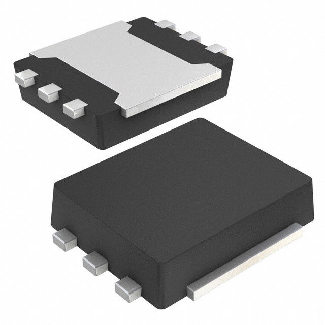
| 产品图片 |
|
| rohs | 符合RoHS无铅 / 符合限制有害物质指令(RoHS)规范要求 |
| 产品系列 | 电源管理 IC,低压差稳压器,Texas Instruments LP38501ATJ-ADJ/NOPB- |
| 数据手册 | |
| 产品型号 | LP38501ATJ-ADJ/NOPB |
| PSRR/纹波抑制—典型值 | 58 dB |
| 产品 | Low Dropout Linear Regulator |
| 产品目录页面 | |
| 产品种类 | 低压差稳压器 |
| 供应商器件封装 | TO-263-5 薄型 |
| 其它名称 | *LP38501ATJ-ADJ/NOPB |
| 包装 | 剪切带 (CT) |
| 商标 | Texas Instruments |
| 回动电压—最大值 | 665 mV |
| 安装类型 | 表面贴装 |
| 安装风格 | SMD/SMT |
| 封装 | Reel |
| 封装/外壳 | TO-263-5 薄型 |
| 封装/箱体 | TO-263-5 |
| 工作温度 | -40°C ~ 125°C |
| 工厂包装数量 | 1000 |
| 最大工作温度 | + 125 C |
| 最大输入电压 | 5.5 V |
| 最小工作温度 | - 40 C |
| 最小输入电压 | 2.7 V |
| 标准包装 | 1 |
| 电压-跌落(典型值) | 0.42V @ 3A |
| 电压-输入 | 2.7 V ~ 5.5 V |
| 电压-输出 | 0.6 V ~ 5 V |
| 电流-输出 | 3A |
| 电流-限制(最小值) | - |
| 稳压器拓扑 | 正,可调式 |
| 稳压器数 | 1 |
| 类型 | LDO Linear Regulator |
| 系列 | LP38501-ADJ |
| 线路调整率 | 0.05 % |
| 负载调节 | 0.24 % |
| 输出电压 | 5 V |
| 输出电压容差 | 1.5 % |
| 输出电流 | 3 A |
| 输出端数量 | 1 Output |
| 输出类型 | Adjustable |
| 配用 | /product-detail/zh/LP38501ATJ-EV/LP38501ATJ-EV-ND/1867892 |


- 商务部:美国ITC正式对集成电路等产品启动337调查
- 曝三星4nm工艺存在良率问题 高通将骁龙8 Gen1或转产台积电
- 太阳诱电将投资9.5亿元在常州建新厂生产MLCC 预计2023年完工
- 英特尔发布欧洲新工厂建设计划 深化IDM 2.0 战略
- 台积电先进制程称霸业界 有大客户加持明年业绩稳了
- 达到5530亿美元!SIA预计今年全球半导体销售额将创下新高
- 英特尔拟将自动驾驶子公司Mobileye上市 估值或超500亿美元
- 三星加码芯片和SET,合并消费电子和移动部门,撤换高东真等 CEO
- 三星电子宣布重大人事变动 还合并消费电子和移动部门
- 海关总署:前11个月进口集成电路产品价值2.52万亿元 增长14.8%


PDF Datasheet 数据手册内容提取
Product Sample & Technical Tools & Support & Folder Buy Documents Software Community LP38501-ADJ,LP38503-ADJ SNVS522I–AUGUST2007–REVISEDAUGUST2015 LP3850x-ADJ, LP3850xA-ADJ 3-A FlexCap Low Dropout Linear Regulator for 2.7-V to 5.5-V Inputs 1 Features 3 Description • InputVoltage:2.7Vto5.5V TI's FlexCap low-dropout (LDO) linear regulators 1 feature unique compensation that allow use of any • AdjustableOutputVoltage:0.6Vto5V type of output capacitor with no limits on minimum or • FlexCap:StablewithCeramic,Tantalum,or maximum equivalent series resistance (ESR). The AluminumCapacitors LP38501 and LP38503 series of LDOs operate from • StableWith10-µFInputandOutputCapacitors a 2.7-V to 5.5-V input supply. These ultra-low-dropout linear regulators respond very quickly to step • LowGround-PinCurrent changesinload,makingthemsuitableforlow-voltage • 25-nAQuiescentCurrentinShutdownMode microprocessor applications. Developed on a CMOS • EnsuredOutputCurrentof3A process (utilizing a PMOS pass transistor) the LP38501-ADJ and LP38503-ADJ have low quiescent • EnsuredV Accuracyof±1.5%at25°C(A ADJ currentsthatchangelittlewithloadcurrent. Grade) • GND Pin Current: Typically 2 mA at 3-A load • EnsuredAccuracyof ±3.5%at25°C(STD) current. • OvertemperatureandOvercurrentProtection • Disable Mode: Typically 25-nA quiescent current • ENABLE(EN)Pin(LP38501only) whentheENpinispulledlow. • –40°Cto+125°COperatingTemperatureRange • Simplified Compensation: Stable with any type of outputcapacitor,regardlessofESR. 2 Applications • Precision Output: A grade versions available with 1.5% V tolerance (25°C) and 3% over line, • ASICPowerSuppliesIn: ADJ load,andtemperature. – Printers,GraphicsCards,DVDPlayers – SetTopBoxes,Copiers,Routers DeviceInformation(1) • DSPandFPGAPowerSupplies PARTNUMBER PACKAGE BODYSIZE(NOM) • SMPSRegulator LP38501 DDPAK/TO-263(5) 10.16mmx8.42mm • Conversionfrom3.3-Vor5-VRail LP38503 TO-263(5) 10.16mmx9.85mm (1) For all available packages, see the orderable addendum at theendofthedatasheet. TypicalApplicationCircuits *Minimumcapacitancerequired(seeApplicationandImplementation). *Minimumcapacitancerequired(seeApplicationandImplementation). 1 An IMPORTANT NOTICE at the end of this data sheet addresses availability, warranty, changes, use in safety-critical applications, intellectualpropertymattersandotherimportantdisclaimers.PRODUCTIONDATA.
LP38501-ADJ,LP38503-ADJ SNVS522I–AUGUST2007–REVISEDAUGUST2015 www.ti.com Table of Contents 1 Features.................................................................. 1 7.4 DeviceFunctionalModes........................................14 2 Applications........................................................... 1 8 ApplicationandImplementation........................ 15 3 Description............................................................. 1 8.1 ApplicationInformation............................................15 4 RevisionHistory..................................................... 2 8.2 TypicalApplications ...............................................15 5 PinConfigurationsandFunctions....................... 3 9 PowerSupplyRecommendations...................... 18 6 Specifications......................................................... 4 10 Layout................................................................... 19 6.1 AbsoluteMaximumRatings......................................4 10.1 LayoutGuidelines.................................................19 6.2 ESDRatings..............................................................4 10.2 LayoutExamples...................................................19 6.3 RecommendedOperatingConditions.......................4 11 DeviceandDocumentationSupport................. 20 6.4 ThermalInformation..................................................4 11.1 DocumentationSupport........................................20 6.5 ElectricalCharacteristics...........................................5 11.2 CommunityResources..........................................20 6.6 TypicalCharacteristics..............................................7 11.3 Trademarks...........................................................20 7 DetailedDescription.............................................. 9 11.4 ElectrostaticDischargeCaution............................20 7.1 Overview...................................................................9 11.5 Glossary................................................................20 7.2 FunctionalBlockDiagrams.......................................9 12 Mechanical,Packaging,andOrderable Information........................................................... 20 7.3 FeatureDescription...................................................9 4 Revision History NOTE:Pagenumbersforpreviousrevisionsmaydifferfrompagenumbersinthecurrentversion. ChangesfromRevisionH(April2013)toRevisionI Page • AddedDeviceInformationandPinConfigurationandFunctionssections,ESDRatingandupdatedThermal Informationtables,FeatureDescription,DeviceFunctionalModes,ApplicationandImplementation,PowerSupply Recommendations,Layout,DeviceandDocumentationSupport,andMechanical,Packaging,andOrderable Informationsections;removeleadtempfromAbsMaxtable(inPOA);removeobsoleteheatsinkingcontent;update thermalvalues........................................................................................................................................................................ 1 • DeletedobsoleteheatsinkinginformationforDDPAK/TO-263package ............................................................................. 18 ChangesfromRevisionG(April2013)toRevisionH Page • ChangedlayoutofNationaldatasheettoTIformat.............................................................................................................. 1 2 SubmitDocumentationFeedback Copyright©2007–2015,TexasInstrumentsIncorporated ProductFolderLinks:LP38501-ADJ LP38503-ADJ
LP38501-ADJ,LP38503-ADJ www.ti.com SNVS522I–AUGUST2007–REVISEDAUGUST2015 5 Pin Configurations and Functions KTTPackage(LP38501) KTTPackage(LP38503) 5-PinDDPAK/TO-263 5-PinDDPAK/TO-263 TopView TopView NDQPackage(LP38501) NDQPackage(LP38503) 5-PinTO-263 5-PinTO-263 TopView TopView PinFunctions PIN LP38501 LP38503 LP38501 LP38503 TYPE DESCRIPTION NAME DDPAK/TO-263 TO-263 ADJ 5 5 5 5 O Setsoutputvoltage. Enable(LP38501-ADJonly).Pullhightoenabletheoutput, EN 1 — 1 — I lowtodisabletheoutput.Thispinhasnointernalbiasand mustbeeithertiedtotheinputvoltage,oractivelydriven. GND 3 3 3 3 G Ground IN 2 2 2 2 I Inputsupplypin. IntheLP38503-ADJ,thispinhasnointernalconnections.It N/C — 1 — 1 — canbeleftfloatingorusedfortracerouting. OUT 4 4 4 4 O Regulatedoutputvoltagepin. TheDAPisusedasathermalconnectiontoremoveheatfrom thedevicetothecircuitboardDAPcoppercladareawhich DAP √ √ √ √ — actsastheheatsink.TheDAPiselectricallyconnectedtothe backsideofthedie.TheDAPmustbeconnectedtoground potential,butcannotbeusedastheonlygroundconnection. Copyright©2007–2015,TexasInstrumentsIncorporated SubmitDocumentationFeedback 3 ProductFolderLinks:LP38501-ADJ LP38503-ADJ
LP38501-ADJ,LP38503-ADJ SNVS522I–AUGUST2007–REVISEDAUGUST2015 www.ti.com 6 Specifications 6.1 Absolute Maximum Ratings overoperatingfree-airtemperaturerange(unlessotherwisenoted)(1) MIN MAX UNIT INpinvoltage(survival) −0.3 6 V ENpinvoltage(survival) −0.3 6 V OUTpinvoltage(survival) −0.3 6 V I (survival) Internallylimited OUT Powerdissipation(2) Internallylimited Storagetemperature,T −65 150 °C stg (1) StressesbeyondthoselistedunderAbsoluteMaximumRatingsmaycausepermanentdamagetothedevice.Thesearestressratings only,whichdonotimplyfunctionaloperationofthedeviceattheseoranyotherconditionsbeyondthoseindicatedunderRecommended OperatingConditions.Exposuretoabsolute-maximum-ratedconditionsforextendedperiodsmayaffectdevicereliability. (2) Operatingjunctiontemperaturemustbeevaluated,andderatedasneeded,basedonambienttemperature(T ),powerdissipation(P ), A D maximumallowableoperatingjunctiontemperature(T )),andpackagethermalresistance(R ).SeeApplicationand J(MAX θJA Implementation. 6.2 ESD Ratings VALUE UNIT V Electrostaticdischarge Humanbodymodel(HBM),perANSI/ESDA/JEDECJS-001,allpins(1) ±2000 V ESD (1) JEDECdocumentJEP155statesthat500-VHBMallowssafemanufacturingwithastandardESDcontrolprocess. 6.3 Recommended Operating Conditions overoperatingfree-airtemperaturerange(unlessotherwisenoted)(1) MIN NOM MAX UNIT Inputsupplyvoltage 2.7 5.5 V Enableinputvoltage 0 5.5 V Outputcurrent(DC) 0 3 A V 0.6 5 V OUT Junctiontemperature(2) −40 125 °C (1) StressesbeyondthoselistedunderAbsoluteMaximumRatingsmaycausepermanentdamagetothedevice.Thesearestressratings only,whichdonotimplyfunctionaloperationofthedeviceattheseoranyotherconditionsbeyondthoseindicatedunderRecommended OperatingConditions.Exposuretoabsolute-maximum-ratedconditionsforextendedperiodsmayaffectdevicereliability. (2) Operatingjunctiontemperaturemustbeevaluated,andderatedasneeded,basedonambienttemperature(T ),powerdissipation(P ), A D maximumallowableoperatingjunctiontemperature(T ),andpackagethermalresistance(R ).SeeApplicationand J(MAX) θJA Implementation. 6.4 Thermal Information LP38501andLP38503 THERMALMETRIC(1) KTT(DDPAK/TO-263) NDQ(TO-263) UNIT 5PINS 5PINS R Junction-to-ambientthermalresistance 41.8 33.3 °C/W θJA R Junction-to-case(top)thermalresistance 45.0 22.1 °C/W θJC(top) R Junction-to-boardthermalresistance 24.8 16.9 °C/W θJB ψ Junction-to-topcharacterizationparameter 13.1 5.8 °C/W JT ψ Junction-to-boardcharacterizationparameter 23.8 16.8 °C/W JB R Junction-to-case(bottom)thermalresistance 2.4 2.3 °C/W θJC(bot) (1) Formoreinformationabouttraditionalandnewthermalmetrics,seetheSemiconductorandICPackageThermalMetricsapplication report,SPRA953. 4 SubmitDocumentationFeedback Copyright©2007–2015,TexasInstrumentsIncorporated ProductFolderLinks:LP38501-ADJ LP38503-ADJ
LP38501-ADJ,LP38503-ADJ www.ti.com SNVS522I–AUGUST2007–REVISEDAUGUST2015 6.5 Electrical Characteristics UnlessotherwisespecifiedV =3.3V,I =10mA,C =10μF,C =10μF,V =V ,V =1.8V.Minimumand IN OUT IN OUT EN IN OUT maximumlimitsapplyoverthejunctiontemperature(T )rangeof–40°Cto+125°Candarespecifiedthroughtest,design,or J statisticalcorrelation.TypicalvaluesrepresentthemostlikelyparametricnormatT =25°C,andareprovidedforreference J purposesonly. PARAMETER TESTCONDITIONS MIN TYP MAX UNIT 2.7V≤V ≤5.5V IN 10mA≤I ≤3A 0.584 0.605 0.626 OUT VADJ ADJpinvoltage(1) TJ=25°C V 2.7V≤V ≤5.5V IN 0.575 0.635 10mA≤I ≤3A OUT 2.7V≤V ≤5.5V IN 10mA≤I ≤3A 0.596 0.605 0.614 OUT VADJ ADJpinvoltage(Agrade)(1) TJ=25°C V 2.7V≤V ≤5.5V IN 0.587 0.623 10mA≤I ≤3A OUT 2.7V≤V ≤5.5V IN 50 nA IADJ ADJpinbiascurrent TJ=25°C 2.7V≤V ≤5.5V 750 nA IN I =3A OUT 420 550 mV VDO Dropoutvoltage(2) TJ=25°C I =3A 665 mV OUT 2.7V≤V ≤5.5V ΔVOUT/ Outputvoltagelineregulation(1)(3) TJ=25°CIN 0.04 %/V ΔV IN 2.7V≤V ≤5.5V 0.05 IN 10mA<I <3A ΔΔVI OUT/ O(4)utputvoltageloadregulation(1) TJ=25°COUT 0.12 %/A OUT 10mA<I <3A 0.24 OUT 10mA<I <3A IGND Goproeurantdionpinmcoudrerentinnormal TJ=25°COUT 2 4 mA 10mA<I <1.5A 5 OUT V <V ,T =25°C 0.025 0.125 EN IL(EN) J I Groundpincurrent µA DISABLED V <V 15 EN IL(EN) I Peakoutputcurrent V ≥V –5% 6 A OUT(PK)GND OUT OUT(NOM) V =0V 6 OUT I Short-circuitcurrent A SC V =0V,T =25°C 3.5 OUT J ENABLEINPUT(LP38501Only) V Enablelogichigh V =ON 1.4 IH(EN) OUT V V Enablelogiclow V =OFF 0.65 IL(EN) OUT TimefromV <V toV =OFF t Turnoffdelay EN IL(EN) OUT 25 µs d(off) I =3A LOAD TimefromV >V toV =ON t Turnondelay EN IH(EN) OUT 25 µs d(on) I =3A LOAD I Enablepinhighcurrent V =V 35 IH(EN) EN IN nA I Enablepinlowcurrent V =0V 35 IL(EN) EN (1) Thelineandloadregulationspecificationcontainsonlythetypicalnumber.However,thelimitsforlineandloadregulationareincluded intheadjustvoltagetolerancespecification. (2) Dropoutvoltageisdefinedastheminimuminputtooutputdifferentialvoltageatwhichtheoutputdrops2%belowthenominalvalue.For anyoutputvoltagelessthan2.5V,theminimumVINoperatingvoltageisthelimitingfactor. (3) Outputvoltagelineregulationisdefinedasthechangeinoutputvoltagefromthenominalvalueduetochangeintheinputlinevoltage. (4) Outputvoltageloadregulationisdefinedasthechangeinoutputvoltagefromthenominalvalueduetochangeintheloadcurrent. Copyright©2007–2015,TexasInstrumentsIncorporated SubmitDocumentationFeedback 5 ProductFolderLinks:LP38501-ADJ LP38503-ADJ
LP38501-ADJ,LP38503-ADJ SNVS522I–AUGUST2007–REVISEDAUGUST2015 www.ti.com Electrical Characteristics (continued) UnlessotherwisespecifiedV =3.3V,I =10mA,C =10μF,C =10μF,V =V ,V =1.8V.Minimumand IN OUT IN OUT EN IN OUT maximumlimitsapplyoverthejunctiontemperature(T )rangeof–40°Cto+125°Candarespecifiedthroughtest,design,or J statisticalcorrelation.TypicalvaluesrepresentthemostlikelyparametricnormatT =25°C,andareprovidedforreference J purposesonly. PARAMETER TESTCONDITIONS MIN TYP MAX UNIT ACPARAMETERS V =3V,I =3A,ƒ=120Hz 58 IN OUT PSRR Ripplerejection dB V =3V,I =3A,ƒ=1kHz 56 IN OUT ρ Outputnoisedensity ƒ=120Hz,C =10µFCER 1 µV/√Hz n(l/f) OUT BW=100Hz–100kHz e Outputnoisevoltage 100 µV n C =10µFCER (RMS) OUT THERMALS T Thermalshutdown T rising 170 — °C SD J ΔT Thermalshutdownhysteresis T fallingfromT 10 — °C SD J SD 6 SubmitDocumentationFeedback Copyright©2007–2015,TexasInstrumentsIncorporated ProductFolderLinks:LP38501-ADJ LP38503-ADJ
LP38501-ADJ,LP38503-ADJ www.ti.com SNVS522I–AUGUST2007–REVISEDAUGUST2015 6.6 Typical Characteristics Unlessotherwisespecified:T =25°C,V =2.7V,V =V ,C =10µF,C =10µF,I =10mA,V =1.8V. J IN EN IN IN OUT OUT OUT Figure1.NoiseDensity Figure2.NoiseDensity Figure3.IGNDvsLoadCurrent Figure4.IGND(OFF)vsTemperature Figure5.V vsTemperature Figure6.DropoutVoltagevsLoadCurrent ADJ Copyright©2007–2015,TexasInstrumentsIncorporated SubmitDocumentationFeedback 7 ProductFolderLinks:LP38501-ADJ LP38503-ADJ
LP38501-ADJ,LP38503-ADJ SNVS522I–AUGUST2007–REVISEDAUGUST2015 www.ti.com Typical Characteristics (continued) Unlessotherwisespecified:T =25°C,V =2.7V,V =V ,C =10µF,C =10µF,I =10mA,V =1.8V. J IN EN IN IN OUT OUT OUT Figure7.V vsTemperature Figure8.TurnonCharacteristics EN Figure9.LoadRegulationvsTemperature Figure10.PSRR 8 SubmitDocumentationFeedback Copyright©2007–2015,TexasInstrumentsIncorporated ProductFolderLinks:LP38501-ADJ LP38503-ADJ
LP38501-ADJ,LP38503-ADJ www.ti.com SNVS522I–AUGUST2007–REVISEDAUGUST2015 7 Detailed Description 7.1 Overview The LP38501-ADJ and LP38503-ADJ are FlexCap and low-dropout adjustable regulators, the output voltage can be set from 0.6 V to 5 V. Standard regulator features, such as overcurrent and overtemperature protections, are alsoincluded. TheLP38501-ADJandLP38503-ADJcontainseveralfeatures: • Stablewithanytypeofoutputcapacitor • Fastloadtransientresponse • DisableMode(LP38501-ADJonly) 7.2 Functional Block Diagrams Figure11. LP38501-ADJBlockDiagram Figure12. LP38503-ADJBlockDiagram 7.3 Feature Description 7.3.1 StabilityandPhaseMargin Any regulator which operates using a feedback loop must be compensated in such a way as to ensure adequate phase margin, which is defined as the difference between the phase shift and –180 degrees at the frequency wheretheloopgaincrossesunity(0dB).FormostLDOregulators,theESRoftheoutputcapacitorisrequiredto createazerotoaddenoughphaseleadtoensurestableoperation. Figure 13 shows the gain/phase plot of the LP38501-ADJ and LP38503-ADJ with an output of 1.2 V, a 10-µF ceramic output capacitor, delivering 2 A of load current. The unity-gain crossover occurs at 300 kHz, and the phasemarginisabout40° (whichisverystable). Copyright©2007–2015,TexasInstrumentsIncorporated SubmitDocumentationFeedback 9 ProductFolderLinks:LP38501-ADJ LP38503-ADJ
LP38501-ADJ,LP38503-ADJ SNVS522I–AUGUST2007–REVISEDAUGUST2015 www.ti.com Feature Description (continued) Figure13. Gain-BandwidthPlotfor2-ALoad Figure 14 shows the gain and phase with no external load. In this case, the only load is provided by the gain setting resistors (about 12 kΩ total in this test). It is immediately obvious that the unity-gain frequency is significantlylower(droppingtoabout500Hz),atwhichpointthephasemarginis125°. Figure14. Gain-BandwidthPlotforNoLoad The reduction in unity-gain bandwidth as load current is reduced is normal for any LDO regulator using a P-FET orPNPpasstransistor,becausetheyhaveapoleintheloopgainfunctiongivenby: 1 F P 2uSuR uC L OUT (1) Equation 1 calculates how the pole goes to the highest frequency when R is minimum value (maximum load L current). In general, LDOs have maximum bandwidth (and lowest phase margin) at full load current. In the case of the LP38501-ADJ, good phase margin is seen even when using ceramic capacitors with ESR values of only a fewmΩ. 7.3.2 LoadTransientResponse Load transient response is defined as the change in regulated output voltage which occurs as a result of a change in load current. Many applications have loads which vary, and the control loop of the voltage regulator must adjust the current in the pass FET transistor in response to load current changes. For this reason, regulatorswithwiderbandwidthsoftenhavebettertransientresponse. The LP38501-ADJ employs an internal feed-forward design which makes the load transient response much faster than would be predicted simply by loop speed; this feedforward means any voltage changes appearing on the output are coupled through to the high-speed driver used to control the gate of the pass FET along a signal pathusingveryfastFETdevices.Becauseofthis,thepasstransistor’scurrentcanchangeveryquickly. 10 SubmitDocumentationFeedback Copyright©2007–2015,TexasInstrumentsIncorporated ProductFolderLinks:LP38501-ADJ LP38503-ADJ
LP38501-ADJ,LP38503-ADJ www.ti.com SNVS522I–AUGUST2007–REVISEDAUGUST2015 Feature Description (continued) Figure 15 shows the output transient response resulting from a change in load current of 0.1 A – 3 A, and then 3 A – 0.1 A with a load current slew rate of 500 mA/µs. As shown in Figure 15, the resulting change in output voltage is only about 40 mV (peak), which is just slightly over 2% for the 1.8-V output used for this test. This is excellentperformanceforsuchasmalloutputcapacitor. Figure15. LoadTransientResponse:10-µFCeramic,0.5-A/µsDi/Dt When the load current changes much more quickly, the output voltage will show more change because the loop and internal feedforward circuitry are not able to react as fast as the load changes. In such cases, it is the output capacitor which must supply load current during the transition until the loop responds and changes the pass transistor’s drive to deliver the new value of load current. As an example, the slew rate of the load current will be increased to 75 A/μs and the same test will be performed. In Figure 16, it can be seen that the peak excursion of theoutputvoltageduringthetransienthasnowincreasedtoabout200mV,whichisjustslightlyover11%forthe 1.8-Voutput. Figure16. LoadTransientResponse:10-μFCeramic,75A/μsdi/dt A better understanding of the load transient can be obtained when the load’s rising edge is expanded in time scale(Figure16). Figure17. RisingEdge,10-µFCeramic,75A/µsdi/dt Copyright©2007–2015,TexasInstrumentsIncorporated SubmitDocumentationFeedback 11 ProductFolderLinks:LP38501-ADJ LP38503-ADJ
LP38501-ADJ,LP38503-ADJ SNVS522I–AUGUST2007–REVISEDAUGUST2015 www.ti.com Feature Description (continued) Figure 16 shows that the output voltage starts “correcting” back upwards after less than a microsecond, and has fullyreverseddirectionafterabout1.2 µs.Thisveryrapidreactionisaresultofthemaximumloopbandwidth(full load is being delivered) and the feedforward effect kicking on the drive to the FET before feedback gets fully aroundtheloop. Incaseswhereextremelyfastloadchangesoccur,andoutputvoltageregulationbetterthan10%isrequired,the output capacitance must be increased. When selecting capacitors, it must be understood that the better performing ones usually cost the most. For fast changing loads, the internal parasitics of ESR (equivalent series resistance)andESL(equivalentseriesinductance)degradethecapacitor’sabilitytosourcecurrentquicklytothe load.Thebestcapacitortypesfortransientperformanceare(inorder): 1. Multilayer Ceramic: with the lowest values of ESR and ESL, they can have ESR values in the range of a few milliOhms.Disadvantage:capacitancevaluesaboveabout22 µFsignificantlyincreaseincost. 2. Low-ESR Aluminum Electrolytics: these are aluminum types (like OSCON) with a special electrolyte which provides extremely low ESR values, and are the closest to ceramic performance while still providing large amountsofcapacitance.Thesearecheaper(bycapacitance)thanceramic. 3. Solid tantalum: can provide several hundred µF of capacitance, transient performance is slightly worse than OSCONtypecapacitors,cheaperthanceramicinlargevalues. 4. General purpose aluminum electrolytics: cheap and provide a lot of capacitance, but give the worst performance. As a first example, larger values of ceramic capacitance show how much reduction can be obtained from the 200-mV output change (Figure 16) which was seen with only a 10-µF ceramic output capacitor. In Figure 18, the 10-µF output capacitor is increased to 22 µF. The 200-mV transient is reduced to about 160 mV, which is from about11%ofV downtoabout9%. OUT Figure18. 22-µFCeramicOutputCapacitor In Figure 19, the output capacitance is increased to 47 µF ceramic. It can be seen that the output transient is further reduced down to about 120 mV, which is still about 6.6% of the output voltage. This shows that a 5X increase in ceramic capacitance from the original 10 µF only reduced the peak voltage transient amplitude by about40%. Figure19. 47-µFCeramicOutputCapacitor 12 SubmitDocumentationFeedback Copyright©2007–2015,TexasInstrumentsIncorporated ProductFolderLinks:LP38501-ADJ LP38503-ADJ
LP38501-ADJ,LP38503-ADJ www.ti.com SNVS522I–AUGUST2007–REVISEDAUGUST2015 Feature Description (continued) In general, managing load transients is done by paralleling ceramic capacitance with a larger bulk capacitance. In this way, the ceramic can source current during the rapidly changing edge and the bulk capacitor can support theloadcurrentafterthefirstinitialspikeincurrent. In the next test, the same 10-µF ceramic capacitor is paralleled with a general-purpose (less expensive) aluminum electrolytic whose capacitance is 220 µF. As shown in Figure 20, there is a small improvement over the 200 mV peak seen with the 10-µF ceramic capacitor alone. By adding the 220 µF aluminum capacitor, the peakisreducedtoabout160mV(thesamepeakvalueasseenwitha22-µFceramiccapacitoralone). Figure20. 10-µFCeramicParalleledby220-µFGenericAluminumElectrolytic A solid Tantalum works better, so the aluminum electrolytic is replaced by a 220-µF Tantalum (Figure 21). The peak amplitude of the output transient is now reduced to about 130 mV, just slightly less efficient than the value ofthe47-µFceramiccapacitoralone. Figure21. 10-µFCeramicParalleledby220-µFTantalum The OSCON (ultra low ESR) aluminum electrolytic is the best of the electrolytics. Figure 22 shows the output voltagetransientisreduceddowntoabout90mV(about5%ofV )whena220-µFOSCONisaddedtothe10 OUT µF ceramic. This indicates that some kind of ultra-low ESR aluminum electrolytic used in parallel with some ceramic capacitance is probably the best approach for extremely fast transients, but each application must be dialedinforit’sspecificloadrequirements. Copyright©2007–2015,TexasInstrumentsIncorporated SubmitDocumentationFeedback 13 ProductFolderLinks:LP38501-ADJ LP38503-ADJ
LP38501-ADJ,LP38503-ADJ SNVS522I–AUGUST2007–REVISEDAUGUST2015 www.ti.com Feature Description (continued) Figure22. 10-µFCeramicParalleledby220-µFOSCON 7.3.3 DropoutVoltage The dropout voltage of a regulator is defined as the input-to-output differential required by the regulator to keep the output voltage within 2% of the nominal value. For CMOS LDOs, the dropout voltage is the product of the loadcurrentandtheR oftheinternalMOSFETpasselement. DS(on) Because the output voltage is beginning to “drop out” of regulation when it drops by 2%, electrical performance of the device is reduced compared to the values listed in Electrical Characteristics for some parameters (line and loadregulationandPSRRwouldbeaffected). 7.3.4 ReverseCurrentPath The internal MOSFET pass element in the LP38501-ADJ and LP38503-ADJ has an inherent parasitic diode. During normal operation, the input voltage is higher than the output voltage and the parasitic diode is reverse biased. However, if the output is pulled above the input in an application, then current flows from the output to the input as the parasitic diode gets forward biased. The output can be pulled above the input as long as the current in the parasitic diode is limited to 200-mA continuous and 1-A peak. The regulator output pin must not be taken below ground potential. If the LP38501-ADJ and LP38503-ADJ is used in a dual-supply system where the regulatorloadisreturnedtoanegativesupply,theoutputmustbediode-clampedtoground. 7.3.5 Short-CircuitProtection The LP38501-ADJ and LP38503-ADJ contain internal current limiting which reduces output current to a safe value if the output is overloaded or shorted. Depending upon the value of V , thermal limiting may also become IN active as the average power dissipated causes the die temperature to increase to the limit value (about 170°C). The hysteresis of the thermal shutdown circuitry can result in a “cyclic” behavior on the output as the die temperatureheatsandcools. 7.4 Device Functional Modes 7.4.1 EnableOperation(LP38501-ADJOnly) The ENABLE pin (EN) must be actively terminated by either a 10-kΩ pullup resistor to V , or a driver which IN actively pulls high and low (such as a CMOS rail to rail comparator). If active drive is used, the pullup resistor is notrequired.ThispinmustbetiedtoV ifnotused(itmustnotbeleftfloating). IN 14 SubmitDocumentationFeedback Copyright©2007–2015,TexasInstrumentsIncorporated ProductFolderLinks:LP38501-ADJ LP38503-ADJ
LP38501-ADJ,LP38503-ADJ www.ti.com SNVS522I–AUGUST2007–REVISEDAUGUST2015 8 Application and Implementation NOTE Information in the following applications sections is not part of the TI component specification, and TI does not warrant its accuracy or completeness. TI’s customers are responsible for determining suitability of components for their purposes. Customers should validateandtesttheirdesignimplementationtoconfirmsystemfunctionality. 8.1 Application Information The LP38501-ADJ and LP38503-ADJ devices can provide 3-A output current with 2.7-V to 5.5-V input voltage. These ultra-low-dropout linear regulators respond very quickly to step changes in load, making them suitable for low-voltagemicroprocessorapplications.Inputandoutputcapacitorsofatleast10 µFarerequired. 8.2 Typical Applications *Minimumcapacitancerequired(seeDetailedDesignProcedure). Figure23. TypicalCircuit(LP38501) *Minimumcapacitancerequired(seeDetailedDesignProcedure). Figure24. TypicalCircuit(LP38503) 8.2.1 DesignRequirements ForLP3850x-ADJtypicalapplications,usetheparameterslistedinTable1 astheinputparameters. Table1.DesignParameters DESIGNPARAMETERS VALUE Inputvoltage 2.7Vto5.5V Outputvoltage 0.6Vto5V(adjustable) Outputcurrent 3A(maximum) Inputcapacitor 10µF(minimum) Outputcapacitor 10µF(minimum) Copyright©2007–2015,TexasInstrumentsIncorporated SubmitDocumentationFeedback 15 ProductFolderLinks:LP38501-ADJ LP38503-ADJ
LP38501-ADJ,LP38503-ADJ SNVS522I–AUGUST2007–REVISEDAUGUST2015 www.ti.com 8.2.2 DetailedDesignProcedure 8.2.2.1 ExternalCapacitors The LP38501-ADJ and LP38503-ADJ require that at least 10-µF (±20%) capacitors be used at the input and output pins located within one cm of the device. Larger capacitors may be used without limit on size for both C IN and C . Capacitor tolerances such as temperature variation and voltage loading effects must be considered OUT when selecting capacitors to ensure that they provide the minimum required amount of capacitance under all operatingconditionsfortheapplication. In general, ceramic capacitors are best for noise bypassing and transient response because of their ultra low ESR. It must be noted that if ceramics are used, only the types with X5R or X7R dielectric ratings must be used (never Z5U or Y5F). Capacitors which have the Z5U or Y5F characteristics have a drop in capacitance of as much as 50% if their temperature increases from 25°C to 85°C. In addition, the capacitance drops significantly withappliedvoltage:atypicalZ5UorY5Fcapacitorcanloseasmuchas60%ofitsratedcapacitanceifonlyhalf oftheratedvoltageisappliedtoit.Forthesereasons,onlyX5RandX7Rceramicsmustbeused. 8.2.2.2 InputCapacitor All linear regulators can be affected by the source impedance of the voltage which is connected to the input. If the source impedance is too high, the reactive component of the source may affect the control loop’s phase margin. To ensure proper loop operation, the ESR of the capacitor used for C must not exceed 0.5 Ω. Any IN good quality ceramic capacitor meets this requirement, as well as many good quality tantalums. Aluminum electrolytic capacitors may also work, but can possibly have an ESR which increases significantly at cold temperatures. If the ESR of the input capacitor may exceed 0.5 Ω, it is recommended that a 2.2-µF ceramic capacitorbeusedinparallel,asthisassuresstableloopoperation. 8.2.2.3 OutputCapacitor Any type of capacitor may be used for C , with no limitations on minimum or maximum ESR, as long as the OUT minimum amount of capacitance is present. The amount of capacitance can be increased without limit. IncreasingthesizeofC typicallygivesimprovedloadtransientresponse. OUT 8.2.2.4 SettingTheOutputVoltage The output voltage of the LP38501-ADJ and LP38503-ADJ can be set to any value between 0.6 V and 5 V using twoexternalresistorsshownasR1andR2inFigure25. Figure25. SettingOutputVoltage The value of R2 must always be less than or equal to 10 kΩ for good loop compensation. R1 can be selected for agivenV usingthefollowingformula: OUT V =V (1+R1/R2)+I (R1) OUT ADJ ADJ where • V istheadjustpinvoltage ADJ • I isthebiascurrentflowingintotheadjustpin (2) ADJ 16 SubmitDocumentationFeedback Copyright©2007–2015,TexasInstrumentsIncorporated ProductFolderLinks:LP38501-ADJ LP38503-ADJ
LP38501-ADJ,LP38503-ADJ www.ti.com SNVS522I–AUGUST2007–REVISEDAUGUST2015 8.2.2.5 RFI/EMISusceptibility Radio frequency interference (RFI) and electro-magnetic interference (EMI) can degrade any integrated circuit's performance because of the small dimensions of the geometries inside the device. In applications where circuit sources are present which generate signals with significant high frequency energy content (> 1 MHz), care must betakentoensurethatthisdoesnotaffectthedeviceregulator. If RFI/EMI noise is present on the input side of the regulator (such as applications where the input source comes from the output of a switching regulator), good ceramic bypass capacitors must be used at the input pin of the devicetoreducetheamountofEMIconductedintothedevice. If the LP38501-ADJ or LP38503-ADJ output is connected to a load which switches at high speed (such as a clock), the high-frequency current pulses required by the load must be supplied by the capacitors on the device output. Because the bandwidth of the regulator loop is less than 300 kHz, the control circuitry cannot respond to load changes above that frequency. This means the effective output impedance of the device at frequencies above 300 kHz is determined only by the output capacitor(s). Ceramic capacitors provide the best performance inthistypeofapplication. In applications where the load is switching at high speed, the output of the device may need RF isolation from the load. In such cases, it is recommended that some inductance be placed between the output capacitor and the load, and good RF bypass capacitors be placed directly across the load. PCB layout is also critical in high noise environments, because RFI/EMI is easily radiated directly into PC traces. Noisy circuitry must be isolated from clean circuits where possible, and grounded through a separate path. At MHz frequencies, ground planes begin to look inductive and RFI/EMI can cause ground bounce across the ground plane. In multi-layer PC Board applications, care must be taken in layout so that noisy power and ground planes do not radiate directly into adjacentlayerswhichcarryanalogpowerandground. 8.2.2.6 OutputNoise Noiseisspecifiedintwoways: • Spot noise or output noise density is the RMS sum of all noise sources, measured at the regulator output, at a specific frequency (measured with a 1-Hz bandwidth). This type of noise is usually plotted on a curve as a functionoffrequency. • Total output noise or broadband noise is the RMS sum of spot noise over a specified bandwidth, usually severaldecadesoffrequencies. Spot noise is measured in units µV/√Hz or nV/√Hz and total output noise is measured in µV . The primary (RMS) source of noise in low-dropout regulators is the internal reference. In CMOS regulators, noise has a low- frequency component and a high frequency component, which depend strongly on the silicon area and quiescent current. Noise can generally be reduced in two ways: by increasing the transistor area or increasing the reference current.However,enlargingthetransistorsincreasesdiesize,andincreasingthereferencecurrentmeanshigher totalsupplycurrent(GNDpincurrent). 8.2.2.7 PowerDissipation/Heatsinking The maximum power dissipation (P ) of the LP38501-ADJ and LP38503-ADJ is limited by the maximum D(MAX) junction temperature of 125°C, along with the maximum ambient temperature (T ) of the application, and the A(MAX) thermal resistance (R ) of the package. Under all possible conditions, the junction temperature (T ) must be θJA J within the range specified in the Recommended Operating Conditions. The total power dissipation of the device isgivenby: P =((V −V )×I )+(V ×I ) D IN OUT OUT IN GND where • I istheoperatinggroundcurrentofthedevice(specifiedunderElectricalCharacteristics). (3) GND The maximum allowable junction temperature rise (ΔT ) depends on the maximum expected ambient J temperature(T )oftheapplication,andthemaximumallowablejunctiontemperature(T ): A(MAX) J(MAX) ΔT =T −T (4) J J(MAX) A(MAX) The maximum allowable value for junction-to-ambient thermal resistance, R , can be calculated using the θJA formula: R =ΔT /P (5) θJA J D(MAX) Copyright©2007–2015,TexasInstrumentsIncorporated SubmitDocumentationFeedback 17 ProductFolderLinks:LP38501-ADJ LP38503-ADJ
LP38501-ADJ,LP38503-ADJ SNVS522I–AUGUST2007–REVISEDAUGUST2015 www.ti.com The LP38501-ADJ and LP38503-ADJ are available in the DDPAK/TO-263 and TO-263 packages. The thermal resistancedependsontheamountofcopperareaallocatedtoheattransfer. 8.2.3 ApplicationCurves Figure27.TurnonTime Figure26.TurnonTime Figure28.LoadTransientResponse:10-μFCeramic,75A/μsdi/dt 9 Power Supply Recommendations The LP38501-ADJ and LP38503-ADJ devices are designed to operate from an input voltage supply range between 2.7 V and 5.5 V. The input voltage range provides adequate headroom in order for the device to have a regulatedoutput.Thisinputsupplymustbewellregulated.Aninputcapacitorofatleast10 μFisrequired. 18 SubmitDocumentationFeedback Copyright©2007–2015,TexasInstrumentsIncorporated ProductFolderLinks:LP38501-ADJ LP38503-ADJ
LP38501-ADJ,LP38503-ADJ www.ti.com SNVS522I–AUGUST2007–REVISEDAUGUST2015 10 Layout 10.1 Layout Guidelines Good layout practices minimize voltage error and prevent instability which can result from ground loops. The input and output capacitors must be directly connected to the device pins with short traces that have no other currentflowinginthem(Kelvinconnect). The best way to do this is to place the capacitors very near the device and make connections directly to the device pins via short traces on the top layer of the PCB. The regulator ground pin must be connected through viastotheinternalorbacksidegroundplanesothattheregulatorhasasinglepointground. Theexternalresistorswhichsettheoutputvoltagemustalsobelocatedverynearthedevicewithallconnections directly tied via short traces to the pins of the device (Kelvin connect). Do not connect the resistive divider to the loadpointorDCerrorcouldbeinduced. 10.2 Layout Examples R2 EN ADJ Pull-up Resistor R1 IN OUT Input Output Capacitor Capacitor Ground Figure29. LP38501-ADJTO-263Layout R2 N/C ADJ R1 IN OUT Input Output Capacitor Capacitor Ground Figure30. LP38503-ADJTO-263Layout Copyright©2007–2015,TexasInstrumentsIncorporated SubmitDocumentationFeedback 19 ProductFolderLinks:LP38501-ADJ LP38503-ADJ
LP38501-ADJ,LP38503-ADJ SNVS522I–AUGUST2007–REVISEDAUGUST2015 www.ti.com 11 Device and Documentation Support 11.1 Documentation Support 11.1.1 RelatedLinks Table 2 lists quick access links. Categories include technical documents, support and community resources, toolsandsoftware,andquickaccesstosampleorbuy. Table2.RelatedLinks TECHNICAL TOOLS& SUPPORT& PARTS PRODUCTFOLDER SAMPLE&BUY DOCUMENTS SOFTWARE COMMUNITY LP38501-ADJ Clickhere Clickhere Clickhere Clickhere Clickhere LP38503-ADJ Clickhere Clickhere Clickhere Clickhere Clickhere 11.2 Community Resources The following links connect to TI community resources. Linked contents are provided "AS IS" by the respective contributors. They do not constitute TI specifications and do not necessarily reflect TI's views; see TI's Terms of Use. TIE2E™OnlineCommunity TI'sEngineer-to-Engineer(E2E)Community.Createdtofostercollaboration amongengineers.Ate2e.ti.com,youcanaskquestions,shareknowledge,exploreideasandhelp solveproblemswithfellowengineers. DesignSupport TI'sDesignSupport QuicklyfindhelpfulE2Eforumsalongwithdesignsupporttoolsand contactinformationfortechnicalsupport. 11.3 Trademarks E2EisatrademarkofTexasInstruments. Allothertrademarksarethepropertyoftheirrespectiveowners. 11.4 Electrostatic Discharge Caution Thesedeviceshavelimitedbuilt-inESDprotection.Theleadsshouldbeshortedtogetherorthedeviceplacedinconductivefoam duringstorageorhandlingtopreventelectrostaticdamagetotheMOSgates. 11.5 Glossary SLYZ022—TIGlossary. Thisglossarylistsandexplainsterms,acronyms,anddefinitions. 12 Mechanical, Packaging, and Orderable Information The following pages include mechanical, packaging, and orderable information. This information is the most current data available for the designated devices. This data is subject to change without notice and revision of thisdocument.Forbrowser-basedversionsofthisdatasheet,refertotheleft-handnavigation. 20 SubmitDocumentationFeedback Copyright©2007–2015,TexasInstrumentsIncorporated ProductFolderLinks:LP38501-ADJ LP38503-ADJ
PACKAGE OPTION ADDENDUM www.ti.com 9-Jun-2020 PACKAGING INFORMATION Orderable Device Status Package Type Package Pins Package Eco Plan Lead/Ball Finish MSL Peak Temp Op Temp (°C) Device Marking Samples (1) Drawing Qty (2) (6) (3) (4/5) LP38501ATJ-ADJ/NOPB ACTIVE TO-263 NDQ 5 1000 Green (RoHS SN Level-1-260C-UNLIM -40 to 125 LP38501A & no Sb/Br) TJ-ADJ LP38501TJ-ADJ/NOPB ACTIVE TO-263 NDQ 5 1000 Green (RoHS SN Level-1-260C-UNLIM LP38501 & no Sb/Br) TJ-ADJ LP38501TS-ADJ/NOPB ACTIVE DDPAK/ KTT 5 45 Green (RoHS SN Level-3-245C-168 HR -40 to 125 LP38501 TO-263 & no Sb/Br) TS-ADJ LP38501TSX-ADJ/NOPB ACTIVE DDPAK/ KTT 5 500 Green (RoHS SN Level-3-245C-168 HR -40 to 125 LP38501 TO-263 & no Sb/Br) TS-ADJ LP38503ATJ-ADJ/NOPB ACTIVE TO-263 NDQ 5 1000 Green (RoHS SN Level-1-260C-UNLIM -40 to 125 LP38503A & no Sb/Br) TJ-ADJ LP38503TJ-ADJ/NOPB ACTIVE TO-263 NDQ 5 1000 Green (RoHS SN Level-1-260C-UNLIM -40 to 125 LP38503 & no Sb/Br) TJ-ADJ LP38503TS-ADJ/NOPB ACTIVE DDPAK/ KTT 5 45 Green (RoHS SN Level-3-245C-168 HR -40 to 125 LP38503 TO-263 & no Sb/Br) TS-ADJ LP38503TSX-ADJ/NOPB ACTIVE DDPAK/ KTT 5 500 Green (RoHS SN Level-3-245C-168 HR -40 to 125 LP38503 TO-263 & no Sb/Br) TS-ADJ (1) The marketing status values are defined as follows: ACTIVE: Product device recommended for new designs. LIFEBUY: TI has announced that the device will be discontinued, and a lifetime-buy period is in effect. NRND: Not recommended for new designs. Device is in production to support existing customers, but TI does not recommend using this part in a new design. PREVIEW: Device has been announced but is not in production. Samples may or may not be available. OBSOLETE: TI has discontinued the production of the device. (2) RoHS: TI defines "RoHS" to mean semiconductor products that are compliant with the current EU RoHS requirements for all 10 RoHS substances, including the requirement that RoHS substance do not exceed 0.1% by weight in homogeneous materials. Where designed to be soldered at high temperatures, "RoHS" products are suitable for use in specified lead-free processes. TI may reference these types of products as "Pb-Free". RoHS Exempt: TI defines "RoHS Exempt" to mean products that contain lead but are compliant with EU RoHS pursuant to a specific EU RoHS exemption. Green: TI defines "Green" to mean the content of Chlorine (Cl) and Bromine (Br) based flame retardants meet JS709B low halogen requirements of <=1000ppm threshold. Antimony trioxide based flame retardants must also meet the <=1000ppm threshold requirement. (3) MSL, Peak Temp. - The Moisture Sensitivity Level rating according to the JEDEC industry standard classifications, and peak solder temperature. (4) There may be additional marking, which relates to the logo, the lot trace code information, or the environmental category on the device. Addendum-Page 1
PACKAGE OPTION ADDENDUM www.ti.com 9-Jun-2020 (5) Multiple Device Markings will be inside parentheses. Only one Device Marking contained in parentheses and separated by a "~" will appear on a device. If a line is indented then it is a continuation of the previous line and the two combined represent the entire Device Marking for that device. (6) Lead/Ball Finish - Orderable Devices may have multiple material finish options. Finish options are separated by a vertical ruled line. Lead/Ball Finish values may wrap to two lines if the finish value exceeds the maximum column width. Important Information and Disclaimer:The information provided on this page represents TI's knowledge and belief as of the date that it is provided. TI bases its knowledge and belief on information provided by third parties, and makes no representation or warranty as to the accuracy of such information. Efforts are underway to better integrate information from third parties. TI has taken and continues to take reasonable steps to provide representative and accurate information but may not have conducted destructive testing or chemical analysis on incoming materials and chemicals. TI and TI suppliers consider certain information to be proprietary, and thus CAS numbers and other limited information may not be available for release. In no event shall TI's liability arising out of such information exceed the total purchase price of the TI part(s) at issue in this document sold by TI to Customer on an annual basis. Addendum-Page 2
PACKAGE MATERIALS INFORMATION www.ti.com 21-Jul-2015 TAPE AND REEL INFORMATION *Alldimensionsarenominal Device Package Package Pins SPQ Reel Reel A0 B0 K0 P1 W Pin1 Type Drawing Diameter Width (mm) (mm) (mm) (mm) (mm) Quadrant (mm) W1(mm) LP38501ATJ-ADJ/NOPB TO-263 NDQ 5 1000 330.0 24.4 10.6 15.4 2.45 12.0 24.0 Q2 LP38501TJ-ADJ/NOPB TO-263 NDQ 5 1000 330.0 24.4 10.6 15.4 2.45 12.0 24.0 Q2 LP38501TSX-ADJ/NOPB DDPAK/ KTT 5 500 330.0 24.4 10.75 14.85 5.0 16.0 24.0 Q2 TO-263 LP38503ATJ-ADJ/NOPB TO-263 NDQ 5 1000 330.0 24.4 10.6 15.4 2.45 12.0 24.0 Q2 LP38503TJ-ADJ/NOPB TO-263 NDQ 5 1000 330.0 24.4 10.6 15.4 2.45 12.0 24.0 Q2 LP38503TSX-ADJ/NOPB DDPAK/ KTT 5 500 330.0 24.4 10.75 14.85 5.0 16.0 24.0 Q2 TO-263 PackMaterials-Page1
PACKAGE MATERIALS INFORMATION www.ti.com 21-Jul-2015 *Alldimensionsarenominal Device PackageType PackageDrawing Pins SPQ Length(mm) Width(mm) Height(mm) LP38501ATJ-ADJ/NOPB TO-263 NDQ 5 1000 367.0 367.0 35.0 LP38501TJ-ADJ/NOPB TO-263 NDQ 5 1000 367.0 367.0 35.0 LP38501TSX-ADJ/NOPB DDPAK/TO-263 KTT 5 500 367.0 367.0 45.0 LP38503ATJ-ADJ/NOPB TO-263 NDQ 5 1000 367.0 367.0 35.0 LP38503TJ-ADJ/NOPB TO-263 NDQ 5 1000 367.0 367.0 35.0 LP38503TSX-ADJ/NOPB DDPAK/TO-263 KTT 5 500 367.0 367.0 45.0 PackMaterials-Page2
MECHANICAL DATA NDQ0005A TJ5A (Rev F) www.ti.com
MECHANICAL DATA KTT0005B TS5B (Rev D) BOTTOM SIDE OF PACKAGE www.ti.com
IMPORTANTNOTICEANDDISCLAIMER TI PROVIDES TECHNICAL AND RELIABILITY DATA (INCLUDING DATASHEETS), DESIGN RESOURCES (INCLUDING REFERENCE DESIGNS), APPLICATION OR OTHER DESIGN ADVICE, WEB TOOLS, SAFETY INFORMATION, AND OTHER RESOURCES “AS IS” AND WITH ALL FAULTS, AND DISCLAIMS ALL WARRANTIES, EXPRESS AND IMPLIED, INCLUDING WITHOUT LIMITATION ANY IMPLIED WARRANTIES OF MERCHANTABILITY, FITNESS FOR A PARTICULAR PURPOSE OR NON-INFRINGEMENT OF THIRD PARTY INTELLECTUAL PROPERTY RIGHTS. These resources are intended for skilled developers designing with TI products. You are solely responsible for (1) selecting the appropriate TI products for your application, (2) designing, validating and testing your application, and (3) ensuring your application meets applicable standards, and any other safety, security, or other requirements. These resources are subject to change without notice. TI grants you permission to use these resources only for development of an application that uses the TI products described in the resource. Other reproduction and display of these resources is prohibited. No license is granted to any other TI intellectual property right or to any third party intellectual property right. TI disclaims responsibility for, and you will fully indemnify TI and its representatives against, any claims, damages, costs, losses, and liabilities arising out of your use of these resources. TI’s products are provided subject to TI’s Terms of Sale (www.ti.com/legal/termsofsale.html) or other applicable terms available either on ti.com or provided in conjunction with such TI products. TI’s provision of these resources does not expand or otherwise alter TI’s applicable warranties or warranty disclaimers for TI products. Mailing Address: Texas Instruments, Post Office Box 655303, Dallas, Texas 75265 Copyright © 2020, Texas Instruments Incorporated