ICGOO在线商城 > 集成电路(IC) > PMIC - 稳压器 - 线性 > TPS71518DCKR
 Datasheet下载
- 型号: TPS71518DCKR
- 制造商: Texas Instruments
- 库位|库存: xxxx|xxxx
- 要求:
| 数量阶梯 | 香港交货 | 国内含税 |
| +xxxx | $xxxx | ¥xxxx |
查看当月历史价格
查看今年历史价格
TPS71518DCKR产品简介:
ICGOO电子元器件商城为您提供TPS71518DCKR由Texas Instruments设计生产,在icgoo商城现货销售,并且可以通过原厂、代理商等渠道进行代购。 TPS71518DCKR价格参考。Texas InstrumentsTPS71518DCKR封装/规格:PMIC - 稳压器 - 线性, Linear Voltage Regulator IC Positive Fixed 1 Output 1.8V 50mA SC-70-5。您可以下载TPS71518DCKR参考资料、Datasheet数据手册功能说明书,资料中有TPS71518DCKR 详细功能的应用电路图电压和使用方法及教程。
TPS71518DCKR 是 Texas Instruments(德州仪器)推出的一款低功耗、低压差线性稳压器(LDO),属于 PMIC - 稳压器 - 线性分类。该型号具有 1.8V 固定输出电压,输入电压范围为 1.8V 至 5.5V,并支持高达 250mA 的负载电流。以下是其主要应用场景:

1. 便携式电子设备
   TPS71518DCKR 的低静态电流(典型值为 16µA)和小封装尺寸(如 DCK 封装)使其非常适合电池供电的便携式设备,例如手持终端、可穿戴设备(如智能手表或健身追踪器)、蓝牙耳机等。它能够高效地管理电源,延长电池寿命。

2. 微控制器电源供应
   该芯片的稳定输出电压(1.8V)非常适合为现代低功耗微控制器(MCU)提供核心电压。由于其出色的瞬态响应性能,能够在 MCU 工作状态切换时保持电压稳定,避免系统崩溃或误操作。

3. 传感器模块供电
   在物联网(IoT)应用中,TPS71518DCKR 可以为各种低功耗传感器(如温度传感器、加速度计、湿度传感器等)提供稳定的电源支持。其低噪声特性有助于提高传感器数据的精确度。

4. 通信模块供电
   该 LDO 可用于为无线通信模块(如 Zigbee、LoRa 或 NB-IoT 模块)供电。其高 PSRR(电源抑制比)特性可以有效减少射频干扰,确保通信质量。

5. 工业自动化与控制
   在工业环境中,TPS71518DCKR 可为现场总线设备、数据采集模块或其他低功耗电路提供可靠电源。其宽输入电压范围适应了工业场景中可能存在的电压波动。

6. 消费类电子产品
   包括数码相机、电子阅读器、遥控器等需要低功耗和小型化设计的产品,TPS71518DCKR 都能提供理想的电源解决方案。

总之,TPS71518DCKR 凭借其高效能、低功耗和紧凑设计,广泛适用于需要稳定低压电源的各种低功耗应用场景,特别适合对电池寿命和空间有严格要求的设计。
| 参数 | 数值 |
| 产品目录 | 集成电路 (IC)半导体 |
| 描述 | IC REG LDO 1.8V 50MA SC70-5低压差稳压器 50-mA 1.8-V High Input Voltage |
| 产品分类 | |
| 品牌 | Texas Instruments |
| 产品手册 | |
| 产品图片 |
|
| rohs | 符合RoHS无铅 / 符合限制有害物质指令(RoHS)规范要求 |
| 产品系列 | 电源管理 IC,低压差稳压器,Texas Instruments TPS71518DCKR- |
| 数据手册 | |
| 产品型号 | TPS71518DCKR |
| 产品目录页面 | |
| 产品种类 | Regulators - Low Dropout (LDO) |
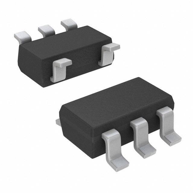
| 供应商器件封装 | SC-70-5 |
| 其它名称 | 296-18731-6 |
| 包装 | Digi-Reel® |
| 单位重量 | 2.500 mg |
| 商标 | Texas Instruments |
| 回动电压—最大值 | 750 mV at 50 mA |
| 安装类型 | 表面贴装 |
| 安装风格 | SMD/SMT |
| 封装 | Reel |
| 封装/外壳 | 6-TSSOP(5 引线),SC-88A,SOT-353 |
| 封装/箱体 | SC-70-5 |
| 工作温度 | -40°C ~ 125°C |
| 工厂包装数量 | 3000 |
| 最大功率耗散 | 0.32 W |
| 最大工作温度 | + 125 C |
| 最大输入电压 | 24 V |
| 最小工作温度 | - 40 C |
| 最小输入电压 | + 2.5 V |
| 标准包装 | 1 |
| 电压-跌落(典型值) | 0.415V @ 50mA |
| 电压-输入 | 2.5 V ~ 24 V |
| 电压-输出 | 1.8V |
| 电压调节准确度 | 4 % |
| 电流-输出 | 50mA |
| 电流-限制(最小值) | 90mA |
| 稳压器拓扑 | 正,固定式 |
| 稳压器数 | 1 |
| 系列 | TPS71518 |
| 线路调整率 | 20 mV |
| 负载调节 | 22 mV |
| 输入偏压电流—最大 | 0.0032 mA |
| 输出电压 | 1.8 V |
| 输出电流 | 50 mA |
| 输出端数量 | 1 Output |
| 输出类型 | Fixed |
| 配用 | /product-detail/zh/TPS71533EVM/296-13590-ND/486548 |


- 商务部:美国ITC正式对集成电路等产品启动337调查
- 曝三星4nm工艺存在良率问题 高通将骁龙8 Gen1或转产台积电
- 太阳诱电将投资9.5亿元在常州建新厂生产MLCC 预计2023年完工
- 英特尔发布欧洲新工厂建设计划 深化IDM 2.0 战略
- 台积电先进制程称霸业界 有大客户加持明年业绩稳了
- 达到5530亿美元!SIA预计今年全球半导体销售额将创下新高
- 英特尔拟将自动驾驶子公司Mobileye上市 估值或超500亿美元
- 三星加码芯片和SET,合并消费电子和移动部门,撤换高东真等 CEO
- 三星电子宣布重大人事变动 还合并消费电子和移动部门
- 海关总署:前11个月进口集成电路产品价值2.52万亿元 增长14.8%


PDF Datasheet 数据手册内容提取
Product Sample & Technical Tools & Support & Folder Buy Documents Software Community TPS715 SLVS338R–MAY2001–REVISEDAPRIL2015 TPS715 50-mA, 24-V, 3.2-μA Supply Current Low-Dropout Linear Regulator in SC70 Package 1 Features 3 Description • 24-VMaximumInputVoltage The TPS715 low-dropout (LDO) voltage regulators 1 offer the benefits of high input voltage, low-dropout • Low3.2-μAQuiescentCurrentat50mA voltage, low-power operation, and miniaturized • StableWithAnyCapacitor≥ 0.47 μF packaging. The devices, which operate over an input • 50-mALow-DropoutRegulator range of 2.5 V to 24 V, are stable with any capacitor greater than or equal to 0.47 μF. The low dropout • Availablein1.8V,1.9V,2.3V,2.5V,3V, voltage and low quiescent current allow operation at 3.3V,3.45V,5V,and extremely low power levels. Therefore, the devices Adjustable(1.2Vto15V) are ideal for powering battery management ICs. • DesignedtoSupportMSP430Families: Specifically, because the devices are enabled as – 1.9-VVersionEnsuredtobeHigherThan soon as the applied voltage reaches the minimum input voltage, the output is quickly available to power MinimumV of1.8V IN continuouslyoperatingbatterychargingICs. – 2.3-VVersionEnsuredtoMeet2.2-VMinimum V forFlashonMSP430F2xx The usual PNP pass transistor has been replaced by IN a PMOS pass element. Because the PMOS pass – 3.45-VVersionEnsuredtobeLowerThan element behaves as a low-value resistor, the low MaximumV of3.6V IN dropout voltage, typically 415mV at 50mA of load – WideVarietyofFixed-OutputVoltageOptions current, is directly proportional to the load current. toMatchV totheMinimumRequiredfor The low quiescent current (3.2 µA typically) is stable IN DesiredMSP430Speed over the entire range of output load current (0 mA to 50mA). • MinimumandMaximumSpecifiedCurrentLimit • 5-PinSC70(DCK) DeviceInformation(1) • –40°Cto+125°CSpecifiedJunction PARTNUMBER PACKAGE BODYSIZE(NOM) TemperatureRange TPS715 SC70(5) 2.00mm×1.25mm • For80-mARatedCurrentandHigherPower (1) For all available packages, see the orderable addendum at Package,seeTPS715A theendofthedatasheet. 2 Applications • UltralowPowerMicrocontrollers • CellularandCordlessHandsets • PortableandBattery-PoweredEquipment TypicalApplicationSchematic TPS715xx IN OUT MSP430 GND Solar Cell 1 An IMPORTANT NOTICE at the end of this data sheet addresses availability, warranty, changes, use in safety-critical applications, intellectualpropertymattersandotherimportantdisclaimers.PRODUCTIONDATA.
TPS715 SLVS338R–MAY2001–REVISEDAPRIL2015 www.ti.com Table of Contents 1 Features.................................................................. 1 8 ApplicationandImplementation........................ 10 2 Applications........................................................... 1 8.1 ApplicationInformation............................................10 3 Description............................................................. 1 8.2 TypicalApplication..................................................10 4 RevisionHistory..................................................... 2 8.3 Do'sandDon'ts.......................................................12 5 PinConfigurationandFunctions......................... 3 9 PowerSupplyRecommendations...................... 12 6 Specifications......................................................... 4 10 Layout................................................................... 13 6.1 AbsoluteMaximumRatings .....................................4 10.1 LayoutGuidelines.................................................13 6.2 ESDRatings ............................................................4 10.2 LayoutExample....................................................13 6.3 RecommendedOperatingConditions.......................4 10.3 PowerDissipation.................................................13 6.4 ThermalInformation..................................................4 11 DeviceandDocumentationSupport................. 14 6.5 ElectricalCharacteristics...........................................5 11.1 DeviceSupport......................................................14 6.6 TypicalCharacteristics..............................................6 11.2 DocumentationSupport .......................................14 7 DetailedDescription.............................................. 8 11.3 Trademarks...........................................................14 7.1 Overview...................................................................8 11.4 ElectrostaticDischargeCaution............................14 7.2 FunctionalBlockDiagrams.......................................8 11.5 Glossary................................................................14 7.3 FeatureDescription...................................................8 12 Mechanical,Packaging,andOrderable Information........................................................... 14 7.4 DeviceFunctionalModes..........................................9 4 Revision History NOTE:Pagenumbersforpreviousrevisionsmaydifferfrompagenumbersinthecurrentversion. ChangesfromRevisionQ(January2014)toRevisionR Page • AddedESDRatingstable,FeatureDescriptionsection,DeviceFunctionalModes,ApplicationandImplementation section,PowerSupplyRecommendationssection,Layoutsection,DeviceandDocumentationSupportsection,and Mechanical,Packaging,andOrderableInformationsection ................................................................................................. 1 • Changedfront-pagefigure..................................................................................................................................................... 1 • ChangedPinConfigurationandFunctionssection;updatedtableformat ............................................................................ 3 • DeletedContinuoustotalpowerdissipationrowinAbsoluteMaximumRatings.................................................................... 4 ChangesfromRevisionP(November2008)toRevisionQ Page • ChangedtestconditionforV accuracyparameter............................................................................................................ 5 OUT 2 SubmitDocumentationFeedback Copyright©2001–2015,TexasInstrumentsIncorporated ProductFolderLinks:TPS715
TPS715 www.ti.com SLVS338R–MAY2001–REVISEDAPRIL2015 5 Pin Configuration and Functions DCKPACKAGE 5-PinSC70 TopView FB/NC 1 5 OUT GND 2 NC 3 4 IN PinFunctions PIN SC70 I/O DESCRIPTION NAME FIXED ADJUSTABLE FB — 1 I Adjustableversiononly.Thisterminalisusedtosettheoutputvoltage. GND 2 2 — Ground IN 4 4 I Inputsupply NC 1,3 3 — Noconnection OUT 5 5 O Outputoftheregulator.Anyoutputcapacitor≥0.47μFcanbeusedforstability. Copyright©2001–2015,TexasInstrumentsIncorporated SubmitDocumentationFeedback 3 ProductFolderLinks:TPS715
TPS715 SLVS338R–MAY2001–REVISEDAPRIL2015 www.ti.com 6 Specifications 6.1 Absolute Maximum Ratings Overoperatingtemperaturerange(unlessotherwisenoted).(1)(2) MIN MAX UNIT V –0.3 24 IN Voltage V V –0.3 16.5 OUT Peakoutputcurrent Internallylimited Junction,T –40 150 J Temperature °C Storage,T –65 150 stg (1) StressesbeyondthoselistedunderAbsoluteMaximumRatingsmaycausepermanentdamagetothedevice.Thesearestressratings only,whichdonotimplyfunctionaloperationofthedeviceattheseoranyotherconditionsbeyondthoseindicatedunderRecommended OperatingConditions.Exposuretoabsolute-maximum-ratedconditionsforextendedperiodsmayaffectdevicereliability. (2) Allvoltagevaluesarewithrespecttonetworkgroundterminal. 6.2 ESD Ratings VALUE UNIT Humanbodymodel(HBM),perANSI/ESDA/JEDECJS-001,allpins(1) ±2000 Electrostatic V(ESD) discharge Cpihnasr(g2)eddevicemodel(CDM),perJEDECspecificationJESD22-C101,all ±500 V (1) JEDECdocumentJEP155statesthat500-VHBMallowssafemanufacturingwithastandardESDcontrolprocess. (2) JEDECdocumentJEP157statesthat250-VCDMallowssafemanufacturingwithastandardESDcontrolprocess. 6.3 Recommended Operating Conditions overoperatingfree-airtemperaturerange(unlessotherwisenoted) MIN NOM MAX UNIT V Inputsupplyvoltage 2.5 24 V IN I Outputcurrent 0 50 mA OUT C Inputcapacitor 0 0.047 µF IN C Outputcapacitor 0.47 1 µF OUT 6.4 Thermal Information TPS715 THERMALMETRIC(1) DCK[SC70] UNIT 5PINS R Junction-to-ambientthermalresistance 253.8 θJA R Junction-to-case(top)thermalresistance 73.7 θJC(top) R Junction-to-boardthermalresistance 84.6 °C/W θJB ψ Junction-to-topcharacterizationparameter 1.1 JT ψ Junction-to-boardcharacterizationparameter 83.9 JB (1) Formoreinformationabouttraditionalandnewthermalmetrics,seetheICPackageThermalMetricsapplicationreport,SPRA953. 4 SubmitDocumentationFeedback Copyright©2001–2015,TexasInstrumentsIncorporated ProductFolderLinks:TPS715
TPS715 www.ti.com SLVS338R–MAY2001–REVISEDAPRIL2015 6.5 Electrical Characteristics Overoperatingjunctiontemperaturerange(T =–40°Cto125°C),V =V +1V,I =1mA,andC =1μF,unless J IN OUT(nom) OUT OUT otherwisenoted.TypicalvaluesareatT =25°C. J PARAMETER TESTCONDITIONS MIN TYP MAX UNIT I =10mA 2.5 24 V Inputvoltage(1) O V IN I =50mA 3 24 O Outputvoltage V 1.2 15 V OUT (TPS71501) V Accuracy(1) OverVIN, VOUT+1V≤VIN≤24V –4% 4% OUT IOUT,andT 100μA≤IOUT≤50mA 0≤I ≤50mA,T =–40°Cto85°C 3.2 4.2 OUT J I Groundpincurrent(2) 0mA≤I ≤50mA 3.2 4.8 μA GND OUT 0mA≤I ≤50mA,V =24V 5.8 OUT IN ΔV Loadregulation I =100μAto50mA 22 mV OUT(ΔIOUT) OUT Outputvoltageline ΔVOUT(ΔVIN) regulation (1) VOUT+1V<VIN≤24V 20 60 mV BW=200Hzto100kHz,C =10μF, V Outputnoisevoltage OUT 575 μVrms n I =50mA OUT V =0V,V ≥3.5V 125 750 mA OUT IN I Outputcurrentlimit CL V =0V,V <3.5V 90 750 mA OUT IN Power-supplyripple PSRR f=100kHz,C =10μF 60 dB rejection OUT Dropoutvoltage V I =50mA 415 750 mV DO V =V –0.1V OUT IN OUT(nom) (1) MinimumV =V +V orthevalueshownforInputvoltageinthistable,whicheverisgreater. IN OUT DO (2) SeeFigure10.TheTPS715familyemploysaleakagenullcontrolcircuit.Thiscircuitisactiveonlyifoutputcurrentislessthanpass FETleakagecurrent.Thecircuitistypicallyactivewhenoutputloadislessthan5μA,V isgreaterthan18V,anddietemperatureis IN greaterthan100°C. Copyright©2001–2015,TexasInstrumentsIncorporated SubmitDocumentationFeedback 5 ProductFolderLinks:TPS715
TPS715 SLVS338R–MAY2001–REVISEDAPRIL2015 www.ti.com 6.6 Typical Characteristics 3.320 3.32 3.315 VCIONU=T4=.31VmF 3.31 IOUT=1mA TJ=25°C V V 3.30 − 3.310 − oltageV 3.305 oltageV 3.29 IOUT=50mA Output 3.300 Output 33..2278 − − OUT3.295 OUT 3.26 VIN=4.3V V V COUT=1mF 3.290 3.25 0 10 20 30 40 50 −40−25−105 20 35 50 65 80 95 110125 IO−Output Current−mA TJ−Junction Temperature−°C Figure1.OutputVoltagevsOutputCurrent Figure2.OutputVoltagevsJunctionTemperature 4.5 8 VIN=4.3V Hz VIN=4.3V 4 VIOOUUTT==13m.3FV V/m 67 IOUT=1mA VCOOUUTT==31.3mFV A m(cid:3) − I−Ground Current−GND 23..553 put Spectral Noise Density 12345 IOUT=50mA 2 ut 0 O −40−25−10 5 20 35 50 65 80 95 110125 100 1k 10k 100k TJ−Junction Temperature−°C f−Frequency−Hz Figure3.QuiescentCurrentvsJunctionTemperature Figure4.OutputSpectralNoiseDensityvsFrequency 18 600 1146 VVCIOONUU=TT4==.331.V3mFV V 500 VCIONU=T3=.21VmF ut Impedance−W 112086 TJ=25°C opout ltage−mV 340000 TJ=25T°JC=125°C Outp 4 IOUT=1mA Dro 200 − −Zo 2 DO 100 TJ=−40°C V 0 IOUT=50mA 0 10 100 1k 10k 100k 1M 10M 0 10 20 30 40 50 f−Frequency−Hz IOUT−Output Current−mA Figure5.OutputImpendencevsFrequency Figure6.DropoutVoltagevsOutputCurrent 6 SubmitDocumentationFeedback Copyright©2001–2015,TexasInstrumentsIncorporated ProductFolderLinks:TPS715
TPS715 www.ti.com SLVS338R–MAY2001–REVISEDAPRIL2015 Typical Characteristics (continued) 1 600 0.9 IOUT=50mA VIN=3.2V 500 −Dropooltage−ut VVDO 0000000.......2456783 TJ=−4T0°JC=2T5J°C=125°C V−oltDropout Vage−mVDO 123400000000 IOUT=50mAIOUT=10mA V 0.1 0 0 0 3 6 9 12 15 −40−25−10 5 20 35 50 65 80 95110 125 VIN−Input Voltage−V TJ−Junction Temperature−°C Figure7.TPS71501DropoutVoltagevsInputVoltage Figure8.DropoutVoltagevsJunctionTemperature B 100 d on− 90 VVIONU=T4=.33.V3V cti 80 COUT=10mF Reje 70 TJ=25°C e ppl 60 IOUT=1mA Ri y 50 pl up 40 S er 30 w Po 20 IOUT=50mA − RR 10 S P 0 10 100 1k 10k 100k 1M 10M f−Frequency−Hz Figure9.PowerSupplyRippleRejectionvsFrequency Copyright©2001–2015,TexasInstrumentsIncorporated SubmitDocumentationFeedback 7 ProductFolderLinks:TPS715
TPS715 SLVS338R–MAY2001–REVISEDAPRIL2015 www.ti.com 7 Detailed Description 7.1 Overview The TPS715 family of LDOs consume only 3.2 µA of current while offering a wide input voltage range and low- dropout voltage in a small package. The devices, which operate over an input range of 2.5 V to 24 V, are stable with any capacitor greater than or equal to 0.47 μF. The low quiescent current makes the TPS715 ideal for powering battery management ICs. Specifically, because the TPS715 is enabled as soon as the applied voltage reaches the minimum input voltage, the output is quickly available to power continuously operating battery chargingICs. 7.2 Functional Block Diagrams V(IN) V(OUT) Current Sense Leakage Null ILIM Control Circuit R1 _ + GND FB R2 V = 1.205 V ref Bandgap Reference Figure10. FunctionalBlockDiagram—AdjustableVersion V(IN) V(OUT) Current Sense Leakage Null ILIM Control Circuit R1 _ + GND R2 V = 1.205 V ref Bandgap Reference Figure11. FunctionalBlockDiagram—FixedVersion 7.3 Feature Description 7.3.1 WideSupplyRange Thisdevicehasanoperationalinputsupplyrangeof2.5Vto24V,allowingforawiderangeofapplications.This widesupplyrangeisidealforapplicationsthathaveeitherlargetransientsorhighDCvoltagesupplies. 7.3.2 LowSupplyCurrent This device only requires 3.2 µA (typical) of supply current from –40°C to 85°C and has a maximum current consumptionof5.8µAat –40°Cto125°C. 7.3.3 StableWithAnyCapacitor≥ 0.47 µF Anycapacitor,includingbothceramicandtantalum,greaterthanorequalto0.47 μFproperlystabilizesthisloop. 8 SubmitDocumentationFeedback Copyright©2001–2015,TexasInstrumentsIncorporated ProductFolderLinks:TPS715
TPS715 www.ti.com SLVS338R–MAY2001–REVISEDAPRIL2015 Feature Description (continued) 7.3.4 InternalCurrentLimit TheinternalcurrentlimitcircuitisusedtoprotecttheLDOagainsthigh-loadcurrentfaultsorshortingevents.The LDO is not designed to operate in a steady-state current limit. During a current limit event, the LDO sources constantcurrent.Therefore,theoutputvoltagefallswhenloadimpedancedecreases. NOTE if a current limit occurs and the resulting output voltage is low, excessive power is dissipatedacrosstheLDO,resultinginpossibledamagetothedevice. 7.3.5 ReverseCurrent The TPS715 PMOS-pass transistor has a built-in back diode that conducts current when the input voltage drops belowtheoutputvoltage(forexample,duringpowerdown).Currentisconductedfromtheoutputtotheinputand isnotinternallylimited.Ifextendedreversevoltageoperationisanticipated,externallimitingmayberequired. 7.4 Device Functional Modes Table1providesaquickcomparisonbetweenthenormal,dropout,anddisabledmodesofoperation. Table1.DeviceFunctionalModeComparison PARAMETER OPERATINGMODE V I IN OUT Normal V >V +V I <I IN OUT(nom) DO OUT CL Dropout V <V +V I <I IN OUT(nom) DO OUT CL Disabled — — 7.4.1 NormalOperation Thedeviceregulatestothenominaloutputvoltageunderthefollowingconditions: • Theinputvoltageisgreaterthanthenominaloutputvoltageplusthedropoutvoltage(V +V ). OUT(nom) DO • Theoutputcurrentislessthanthecurrentlimit(I <I ). OUT CL • Thedevicejunctiontemperatureislessthan125°C. 7.4.2 DropoutOperation If the input voltage is lower than the nominal output voltage plus the specified dropout voltage, but all other conditions are met for normal operation, the device operates in dropout mode. In this mode, the output voltage tracks the input voltage. During this mode, the transient performance of the device becomes significantly degraded because the pass device is in the linear region and no longer controls the current through the LDO. Lineorloadtransientsindropoutcanresultinlargeoutput-voltagedeviations. Copyright©2001–2015,TexasInstrumentsIncorporated SubmitDocumentationFeedback 9 ProductFolderLinks:TPS715
TPS715 SLVS338R–MAY2001–REVISEDAPRIL2015 www.ti.com 8 Application and Implementation NOTE Information in the following applications sections is not part of the TI component specification, and TI does not warrant its accuracy or completeness. TI’s customers are responsible for determining suitability of components for their purposes. Customers should validateandtesttheirdesignimplementationtoconfirmsystemfunctionality. 8.1 Application Information The TPS715 family of LDO regulators has been optimized for ultralow-power applications such as the MSP430 microcontroller.Theultralow-supplycurrentoftheTPS715devicemaximizesefficiencyatlightloads,anditshigh inputvoltagerangemakesitsuitableforsuppliessuchasunconditionedsolarpanels. 8.2 Typical Application TPS71533 VIN IN OUT VOUT C1 GND 0.47mF 0.1mF Figure12. TypicalApplicationCircuit(Fixed-VoltageVersion) OUTPUT VOLTAGE PROGRAMMING GUIDE VIN IN OUT VOUT OUTPUT TPS71501 R1 CFB VOLTAGE R1 R2 0.1mF 0.47mF GND FB 1.8 V 0.499 MW 1 MW R 2.8 V 1.33 MW 1 MW 2 5.0 V 3.16 MW 1 MW VOUT=VREF´æçè1+RR21ö÷ø Figure13. TPS71501AdjustableLDORegulatorProgramming 8.2.1 DesignRequirements 8.2.1.1 PowertheMSP430Microcontroller Several versions of the TPS715 are ideal for powering the MSP430 microcontroller. Table 2 shows potential applicationsofsomevoltageversions. Table2.TypicalMSP430Applications DEVICE V (TYP) APPLICATION OUT TPS71519 1.9V V >1.8VrequiredbymanyMSP430s.Allowslowestpowerconsumptionoperation. OUT(min) TPS71523 2.3V V >2.2VrequiredbysomeMSP430sflashoperation. OUT(min) TPS71530 3V V >2.7VrequiredbysomeMSP430sFlashoperation. OUT(min) TPS715345 3.45V V <3.6VrequiredbysomeMSP430s.Allowshighestspeedoperation. OUT(max) The TPS715 family offers many output voltage versions to allow designers to optimize the supply voltage for the MSP430,therebyminimizingthesupplycurrentconsumedbytheMSP430. 10 SubmitDocumentationFeedback Copyright©2001–2015,TexasInstrumentsIncorporated ProductFolderLinks:TPS715
TPS715 www.ti.com SLVS338R–MAY2001–REVISEDAPRIL2015 8.2.2 DetailedDesignProcedure 8.2.2.1 ExternalCapacitorRequirements Although not required, a 0.047-μF or larger input bypass capacitor, connected between IN and GND and located close to the device, is recommended to improve transient response and noise rejection of the power supply as a whole.Ahigher-valueinputcapacitormaybenecessaryiflarge,fast-rise-timeloadtransientsareanticipatedand thedeviceislocatedseveralinchesfromthepowersource. TheTPS715requiresanoutputcapacitorconnectedbetweenOUTandGNDtostabilizetheinternalcontrolloop. Anycapacitor(includingceramicandtantalum)greaterthanorequalto0.47 μFproperlystabilizesthisloop.X7R or X5R type capacitors are recommended due to their wider temperature spec and lower temperature coefficient, butothertypesofcapacitorsmaybeused. 8.2.2.2 DropoutVoltage(V ) DO Generally speaking, the dropout voltage often refers to the voltage difference between the input and output voltage (V = V – V ). However, in the Electrical Characteristics, V is defined as the V – V voltage at DO IN OUT DO IN OUT the rated current, where the pass-FET is fully on in the ohmic region of operation and is characterized by the classic R of the FET. V indirectly specifies a minimum input voltage above the nominal programmed DS(on) DO output voltage at which the output voltage is expected to remain within its accuracy boundary. If the input falls belowthisV limit(V <V +V ),thentheoutputvoltagedecreasesinordertofollowtheinputvoltage. DO IN OUT DO Dropout voltage is always determined by the R of the main pass-FET. Therefore, if the LDO operates below DS(on) theratedcurrent,thentheV forthatcurrentscalesaccordingly.R canbecalculatedusingEquation1: DO DS(on) V R = DO DS(ON) I RATED (1) 8.2.2.3 SettingV fortheTPS71501AdjustableLDO OUT The TPS715 family contains an adjustable-version, TPS71501, which sets the output voltage using an external resistor divider as shown in Figure 13. The output voltage operating range is 1.2 V to 15 V, and is calculated using: æ R1ö VOUT = VREF´çè1+R2÷ø where • V =1.205V(typical) (2) REF Resistors R1 and R2 should be chosen to allow approximately 1.5-μA of current through the resistor divider. Lower value resistors can be used for improved noise performance, but will consume more power. Higher resistor values should be avoided as leakage current into or out of FB across R1/R2 creates an offset voltage that is proportional to V divided by V . The recommended design procedure is to choose R2 = 1MΩ to set OUT REF thedividercurrentat1.5 μA,andthencalculateR1usingEquation3: æV ö R1=ç OUT -1÷´2 V è REF ø (3) Figure13showsthisconfiguration. Copyright©2001–2015,TexasInstrumentsIncorporated SubmitDocumentationFeedback 11 ProductFolderLinks:TPS715
TPS715 SLVS338R–MAY2001–REVISEDAPRIL2015 www.ti.com 8.2.3 ApplicationCurves 8 V V−Ooltautput Vge−VOUTV−Input oltage−VVIN 7642153 VVRCINOLOUU=TT6==631W.03VmOVFUT ∆V−Change inut oltage−VVOUTOutpoltaut Vge−m−155050.0030 VICOOOUUUTTT===5310.03mmVAF 0 np 4.3 I 0 2 4 6 8 10 12 14 16 18 20 −N 0 50100 150 200250300 350 400450500 t−Time−ms VI t−Time−ms Figure14.PowerUpandPowerDown Figure15.LineTransientResponse V nm V = 4.3 V Change ioltage- 420000 VCIOONUUTT== 31.03 mVF VD-OUTutput V 0 O -200 A m - 60 Output Current- UT 420000 100 2003004t0−0T5im00e−60m0s7008009001000 O I Figure16.LoadTransientResponse 8.3 Do's and Don'ts Placeatleastone0.47-µFcapacitorascloseaspossibletotheOUTandGNDterminalsoftheregulator. Donotconnecttheoutputcapacitortotheregulatorusingalong,thintrace. Connect an input capacitor as close as possible to the IN and GND terminals of the regulator for best performance. Donotexceedtheabsolutemaximumratings. 9 Power Supply Recommendations The TPS715 is designed to operate from an input voltage supply range between 2.5 V and 24 V. The input voltage range provides adequate headroom in order for the device to have a regulated output. This input supply mustbewellregulated.Iftheinputsupplyisnoisy,additionalinputcapacitorswithlowESRcanhelpimprovethe outputnoiseperformance. 12 SubmitDocumentationFeedback Copyright©2001–2015,TexasInstrumentsIncorporated ProductFolderLinks:TPS715
TPS715 www.ti.com SLVS338R–MAY2001–REVISEDAPRIL2015 10 Layout 10.1 Layout Guidelines For best overall performance, place all circuit components on the same side of the printed-circuit-board and as nearaspracticaltotherespectiveLDOpinconnections.Placegroundreturnconnectionsfortheinputandoutput capacitors as close to the GND pin as possible, using wide, component-side, copper planes. TI strongly discourages using vias and long traces to create LDO circuit connections to the input capacitor, output capacitor, or the resistor divider because that will negatively affect system performance. This grounding and layout scheme minimizes inductive parasitics, and thereby reduces load-current transients, minimizes noise, and increases circuit stability. A ground reference plane is also recommended and is either embedded in the PCB itself or locatedonthebottomsideofthePCBoppositethecomponents.Thisreferenceplaneservestoassureaccuracy oftheoutputvoltageandshieldtheLDOfromnoise. 10.2 Layout Example GND R2 NC GND FB CIN TPS71501DCK R1 VIN IN OUT COUT GND VOUT Figure17. ExampleLayoutforTPS71501DCK 10.3 Power Dissipation Toensurereliableoperation,worst-casejunctiontemperatureshouldnotexceed125°C.Thisrestrictionlimitsthe power dissipation the regulator can handle in any given application. To ensure the junction temperature is within acceptable limits, calculate the maximum allowable dissipation, P , and the actual dissipation, P , which D(max) D mustbelessthanorequaltoP . D(max) Themaximum-power-dissipationlimitisdeterminedusingEquation4: T max-T P = J A D(max) R qJA where • Tmaxisthemaximumallowablejunctiontemperature J • R isthethermalresistancejunction-to-ambientforthepackage(seetheThermalInformationtable) θJA • T istheambienttemperature (4) A TheregulatordissipationiscalculatedusingEquation5: P =(V -V )´I D IN OUT OUT (5) ForahigherpowerpackageversionoftheTPS715,seetheTPS715A. Copyright©2001–2015,TexasInstrumentsIncorporated SubmitDocumentationFeedback 13 ProductFolderLinks:TPS715
TPS715 SLVS338R–MAY2001–REVISEDAPRIL2015 www.ti.com 11 Device and Documentation Support 11.1 Device Support 11.1.1 DevelopmentSupport 11.1.1.1 EvaluationModule An evaluation module (EVM) is available to assist in the initial circuit performance evaluation using the TPS715. The TPS71533EVM evaluation module (and related user's guide) can be requested at the TI website through the productfoldersorpurchaseddirectlyfromtheTIeStore. 11.1.1.2 SpiceModels Computer simulation of circuit performance using SPICE is often useful when analyzing the performance of analog circuits and systems. A SPICE model for the TPS715 is available through the product folders under Tools &Software. 11.1.2 DeviceNomenclature Table3.DeviceNomenclature(1) PRODUCT V (2) OUT XXisnominaloutputvoltage(forexample,28=2.8V,285=2.85V,01=Adjustable). TPS715xxyyyz YYYispackagedesignator. Zispackagequantity. (1) ForthemostcurrentpackageandorderinginformationseethePackageOptionAddendumattheendofthisdocument,orseetheTI websiteatwww.ti.com. (2) Outputvoltagesfrom1.25Vto5.4Vin50-mVincrementsareavailablethroughtheuseofinnovativefactoryEEPROMprogramming; minimumorderquantitiesmayapply.Contactfactoryfordetailsandavailability. 11.2 Documentation Support 11.2.1 RelatedDocumentation Forrelateddocumentationseethefollowing: • TPS71533EVMLDOEvaluationModuleUserGuide,SLVU061 • TPS735:HighInputVoltage,MicropowerSON-Packaged,80-mALDOLinearRegulators,SBVS047 11.3 Trademarks Alltrademarksarethepropertyoftheirrespectiveowners. 11.4 Electrostatic Discharge Caution Thesedeviceshavelimitedbuilt-inESDprotection.Theleadsshouldbeshortedtogetherorthedeviceplacedinconductivefoam duringstorageorhandlingtopreventelectrostaticdamagetotheMOSgates. 11.5 Glossary SLYZ022—TIGlossary. Thisglossarylistsandexplainsterms,acronyms,anddefinitions. 12 Mechanical, Packaging, and Orderable Information The following pages include mechanical, packaging, and orderable information. This information is the most current data available for the designated devices. This data is subject to change without notice and revision of thisdocument.Forbrowser-basedversionsofthisdatasheet,refertotheleft-handnavigation. 14 SubmitDocumentationFeedback Copyright©2001–2015,TexasInstrumentsIncorporated ProductFolderLinks:TPS715
PACKAGE OPTION ADDENDUM www.ti.com 6-Feb-2020 PACKAGING INFORMATION Orderable Device Status Package Type Package Pins Package Eco Plan Lead/Ball Finish MSL Peak Temp Op Temp (°C) Device Marking Samples (1) Drawing Qty (2) (6) (3) (4/5) HPA00328DCKR ACTIVE SC70 DCK 5 3000 Green (RoHS NIPDAU Level-1-260C-UNLIM -40 to 85 AQI & no Sb/Br) HPA00423DCKR ACTIVE SC70 DCK 5 3000 Green (RoHS NIPDAU Level-1-260C-UNLIM -40 to 125 ARB & no Sb/Br) HPA00681DCKR ACTIVE SC70 DCK 5 3000 Green (RoHS NIPDAU Level-1-260C-UNLIM -40 to 125 ARB & no Sb/Br) TPS71501DCKR ACTIVE SC70 DCK 5 3000 Green (RoHS NIPDAU | NIPDAUAG Level-1-260C-UNLIM -40 to 125 ARB & no Sb/Br) TPS71501DCKRG4 ACTIVE SC70 DCK 5 3000 Green (RoHS NIPDAU Level-1-260C-UNLIM -40 to 125 ARB & no Sb/Br) TPS71518DCKR ACTIVE SC70 DCK 5 3000 Green (RoHS NIPDAUAG Level-1-260C-UNLIM -40 to 125 ARD & no Sb/Br) TPS71518DCKRG4 ACTIVE SC70 DCK 5 3000 Green (RoHS NIPDAUAG Level-1-260C-UNLIM -40 to 125 ARD & no Sb/Br) TPS71519DCKR ACTIVE SC70 DCK 5 3000 Green (RoHS NIPDAUAG Level-1-260C-UNLIM -40 to 125 BOX & no Sb/Br) TPS71523DCKR ACTIVE SC70 DCK 5 3000 Green (RoHS NIPDAU | NIPDAUAG Level-1-260C-UNLIM -40 to 125 BNX & no Sb/Br) TPS71525DCKR ACTIVE SC70 DCK 5 3000 Green (RoHS NIPDAU | NIPDAUAG Level-1-260C-UNLIM -40 to 125 AQL & no Sb/Br) TPS71525DCKRG4 ACTIVE SC70 DCK 5 3000 Green (RoHS NIPDAU Level-1-260C-UNLIM -40 to 125 AQL & no Sb/Br) TPS71530DCKR ACTIVE SC70 DCK 5 3000 Green (RoHS NIPDAU | NIPDAUAG Level-1-260C-UNLIM -40 to 125 AQM & no Sb/Br) TPS71530DCKRG4 ACTIVE SC70 DCK 5 3000 Green (RoHS NIPDAU Level-1-260C-UNLIM -40 to 125 AQM & no Sb/Br) TPS71533DCKR ACTIVE SC70 DCK 5 3000 Green (RoHS NIPDAU | NIPDAUAG Level-1-260C-UNLIM -40 to 125 AQI & no Sb/Br) TPS71533DCKRG4 ACTIVE SC70 DCK 5 3000 Green (RoHS NIPDAU Level-1-260C-UNLIM -40 to 125 AQI & no Sb/Br) TPS715345DCKR ACTIVE SC70 DCK 5 3000 Green (RoHS NIPDAUAG Level-1-260C-UNLIM -40 to 125 BNY & no Sb/Br) TPS71550DCKR ACTIVE SC70 DCK 5 3000 Green (RoHS NIPDAU | NIPDAUAG Level-1-260C-UNLIM -40 to 125 T48 & no Sb/Br) Addendum-Page 1
PACKAGE OPTION ADDENDUM www.ti.com 6-Feb-2020 Orderable Device Status Package Type Package Pins Package Eco Plan Lead/Ball Finish MSL Peak Temp Op Temp (°C) Device Marking Samples (1) Drawing Qty (2) (6) (3) (4/5) TPS71550DCKRG4 ACTIVE SC70 DCK 5 3000 Green (RoHS NIPDAU Level-1-260C-UNLIM -40 to 125 T48 & no Sb/Br) (1) The marketing status values are defined as follows: ACTIVE: Product device recommended for new designs. LIFEBUY: TI has announced that the device will be discontinued, and a lifetime-buy period is in effect. NRND: Not recommended for new designs. Device is in production to support existing customers, but TI does not recommend using this part in a new design. PREVIEW: Device has been announced but is not in production. Samples may or may not be available. OBSOLETE: TI has discontinued the production of the device. (2) RoHS: TI defines "RoHS" to mean semiconductor products that are compliant with the current EU RoHS requirements for all 10 RoHS substances, including the requirement that RoHS substance do not exceed 0.1% by weight in homogeneous materials. Where designed to be soldered at high temperatures, "RoHS" products are suitable for use in specified lead-free processes. TI may reference these types of products as "Pb-Free". RoHS Exempt: TI defines "RoHS Exempt" to mean products that contain lead but are compliant with EU RoHS pursuant to a specific EU RoHS exemption. Green: TI defines "Green" to mean the content of Chlorine (Cl) and Bromine (Br) based flame retardants meet JS709B low halogen requirements of <=1000ppm threshold. Antimony trioxide based flame retardants must also meet the <=1000ppm threshold requirement. (3) MSL, Peak Temp. - The Moisture Sensitivity Level rating according to the JEDEC industry standard classifications, and peak solder temperature. (4) There may be additional marking, which relates to the logo, the lot trace code information, or the environmental category on the device. (5) Multiple Device Markings will be inside parentheses. Only one Device Marking contained in parentheses and separated by a "~" will appear on a device. If a line is indented then it is a continuation of the previous line and the two combined represent the entire Device Marking for that device. (6) Lead/Ball Finish - Orderable Devices may have multiple material finish options. Finish options are separated by a vertical ruled line. Lead/Ball Finish values may wrap to two lines if the finish value exceeds the maximum column width. Important Information and Disclaimer:The information provided on this page represents TI's knowledge and belief as of the date that it is provided. TI bases its knowledge and belief on information provided by third parties, and makes no representation or warranty as to the accuracy of such information. Efforts are underway to better integrate information from third parties. TI has taken and continues to take reasonable steps to provide representative and accurate information but may not have conducted destructive testing or chemical analysis on incoming materials and chemicals. TI and TI suppliers consider certain information to be proprietary, and thus CAS numbers and other limited information may not be available for release. In no event shall TI's liability arising out of such information exceed the total purchase price of the TI part(s) at issue in this document sold by TI to Customer on an annual basis. OTHER QUALIFIED VERSIONS OF TPS715 : •Automotive: TPS715-Q1 Addendum-Page 2
PACKAGE OPTION ADDENDUM www.ti.com 6-Feb-2020 NOTE: Qualified Version Definitions: •Automotive - Q100 devices qualified for high-reliability automotive applications targeting zero defects Addendum-Page 3
PACKAGE MATERIALS INFORMATION www.ti.com 15-Feb-2018 TAPE AND REEL INFORMATION *Alldimensionsarenominal Device Package Package Pins SPQ Reel Reel A0 B0 K0 P1 W Pin1 Type Drawing Diameter Width (mm) (mm) (mm) (mm) (mm) Quadrant (mm) W1(mm) TPS71501DCKR SC70 DCK 5 3000 178.0 9.0 2.4 2.5 1.2 4.0 8.0 Q3 TPS71501DCKR SC70 DCK 5 3000 180.0 8.4 2.41 2.41 1.2 4.0 8.0 Q3 TPS71518DCKR SC70 DCK 5 3000 180.0 8.4 2.41 2.41 1.2 4.0 8.0 Q3 TPS71519DCKR SC70 DCK 5 3000 180.0 8.4 2.41 2.41 1.2 4.0 8.0 Q3 TPS71523DCKR SC70 DCK 5 3000 178.0 9.0 2.4 2.5 1.2 4.0 8.0 Q3 TPS71523DCKR SC70 DCK 5 3000 180.0 8.4 2.41 2.41 1.2 4.0 8.0 Q3 TPS71525DCKR SC70 DCK 5 3000 180.0 8.4 2.41 2.41 1.2 4.0 8.0 Q3 TPS71525DCKR SC70 DCK 5 3000 178.0 9.0 2.4 2.5 1.2 4.0 8.0 Q3 TPS71530DCKR SC70 DCK 5 3000 178.0 9.0 2.4 2.5 1.2 4.0 8.0 Q3 TPS71530DCKR SC70 DCK 5 3000 180.0 8.4 2.41 2.41 1.2 4.0 8.0 Q3 TPS71533DCKR SC70 DCK 5 3000 180.0 8.4 2.41 2.41 1.2 4.0 8.0 Q3 TPS71533DCKR SC70 DCK 5 3000 178.0 9.0 2.4 2.5 1.2 4.0 8.0 Q3 TPS715345DCKR SC70 DCK 5 3000 180.0 8.4 2.41 2.41 1.2 4.0 8.0 Q3 TPS71550DCKR SC70 DCK 5 3000 178.0 9.0 2.4 2.5 1.2 4.0 8.0 Q3 TPS71550DCKR SC70 DCK 5 3000 180.0 8.4 2.41 2.41 1.2 4.0 8.0 Q3 PackMaterials-Page1
PACKAGE MATERIALS INFORMATION www.ti.com 15-Feb-2018 *Alldimensionsarenominal Device PackageType PackageDrawing Pins SPQ Length(mm) Width(mm) Height(mm) TPS71501DCKR SC70 DCK 5 3000 180.0 180.0 18.0 TPS71501DCKR SC70 DCK 5 3000 183.0 183.0 20.0 TPS71518DCKR SC70 DCK 5 3000 183.0 183.0 20.0 TPS71519DCKR SC70 DCK 5 3000 183.0 183.0 20.0 TPS71523DCKR SC70 DCK 5 3000 180.0 180.0 18.0 TPS71523DCKR SC70 DCK 5 3000 183.0 183.0 20.0 TPS71525DCKR SC70 DCK 5 3000 183.0 183.0 20.0 TPS71525DCKR SC70 DCK 5 3000 180.0 180.0 18.0 TPS71530DCKR SC70 DCK 5 3000 180.0 180.0 18.0 TPS71530DCKR SC70 DCK 5 3000 183.0 183.0 20.0 TPS71533DCKR SC70 DCK 5 3000 183.0 183.0 20.0 TPS71533DCKR SC70 DCK 5 3000 180.0 180.0 18.0 TPS715345DCKR SC70 DCK 5 3000 183.0 183.0 20.0 TPS71550DCKR SC70 DCK 5 3000 180.0 180.0 18.0 TPS71550DCKR SC70 DCK 5 3000 183.0 183.0 20.0 PackMaterials-Page2
None
None
IMPORTANTNOTICEANDDISCLAIMER TI PROVIDES TECHNICAL AND RELIABILITY DATA (INCLUDING DATASHEETS), DESIGN RESOURCES (INCLUDING REFERENCE DESIGNS), APPLICATION OR OTHER DESIGN ADVICE, WEB TOOLS, SAFETY INFORMATION, AND OTHER RESOURCES “AS IS” AND WITH ALL FAULTS, AND DISCLAIMS ALL WARRANTIES, EXPRESS AND IMPLIED, INCLUDING WITHOUT LIMITATION ANY IMPLIED WARRANTIES OF MERCHANTABILITY, FITNESS FOR A PARTICULAR PURPOSE OR NON-INFRINGEMENT OF THIRD PARTY INTELLECTUAL PROPERTY RIGHTS. These resources are intended for skilled developers designing with TI products. You are solely responsible for (1) selecting the appropriate TI products for your application, (2) designing, validating and testing your application, and (3) ensuring your application meets applicable standards, and any other safety, security, or other requirements. These resources are subject to change without notice. TI grants you permission to use these resources only for development of an application that uses the TI products described in the resource. Other reproduction and display of these resources is prohibited. No license is granted to any other TI intellectual property right or to any third party intellectual property right. TI disclaims responsibility for, and you will fully indemnify TI and its representatives against, any claims, damages, costs, losses, and liabilities arising out of your use of these resources. TI’s products are provided subject to TI’s Terms of Sale (www.ti.com/legal/termsofsale.html) or other applicable terms available either on ti.com or provided in conjunction with such TI products. TI’s provision of these resources does not expand or otherwise alter TI’s applicable warranties or warranty disclaimers for TI products. Mailing Address: Texas Instruments, Post Office Box 655303, Dallas, Texas 75265 Copyright © 2020, Texas Instruments Incorporated