ICGOO在线商城 > 集成电路(IC) > PMIC - 稳压器 - 线性 > SIP21108DT-T1-E3

 Datasheet下载
- 型号: SIP21108DT-T1-E3
- 制造商: Vishay
- 库位|库存: xxxx|xxxx
- 要求:
| 数量阶梯 | 香港交货 | 国内含税 |
| +xxxx | $xxxx | ¥xxxx |
查看当月历史价格
查看今年历史价格
SIP21108DT-T1-E3产品简介:
ICGOO电子元器件商城为您提供SIP21108DT-T1-E3由Vishay设计生产,在icgoo商城现货销售,并且可以通过原厂、代理商等渠道进行代购。 SIP21108DT-T1-E3价格参考¥询价-¥询价。VishaySIP21108DT-T1-E3封装/规格:PMIC - 稳压器 - 线性, Linear Voltage Regulator IC Positive Adjustable 1 Output Adjustable 150mA TSOT-23-5。您可以下载SIP21108DT-T1-E3参考资料、Datasheet数据手册功能说明书,资料中有SIP21108DT-T1-E3 详细功能的应用电路图电压和使用方法及教程。
Vishay Siliconix的SIP21108DT-T1-E3是一款PMIC(电源管理集成电路),属于线性稳压器类别。它具有低噪声、高精度和高效能的特点,适用于多种需要稳定电压输出的应用场景。

 主要应用场景:
1. 消费电子设备:如智能手机、平板电脑和可穿戴设备。这些设备对电源管理要求较高,需要在小尺寸内实现高效的电源转换和稳定的电压输出。SIP21108DT-T1-E3能够提供稳定的供电,确保设备在各种工作模式下都能正常运行,同时减少发热和功耗。

2. 通信设备:包括路由器、交换机和其他网络设备。这些设备通常需要多个不同电压的电源轨来为不同的组件供电,而SIP21108DT-T1-E3可以为这些设备提供多路输出,并且具备良好的负载响应能力,确保通信信号的稳定性和可靠性。

3. 工业自动化系统:如PLC(可编程逻辑控制器)、传感器和执行器等。工业环境中对电源的稳定性和可靠性要求极高,SIP21108DT-T1-E3可以在宽温度范围内保持稳定的输出电压,适应恶劣的工作环境,保证系统的持续运行。

4. 医疗设备:如便携式医疗仪器、监护仪等。这些设备对电源的精度和稳定性有严格的要求,SIP21108DT-T1-E3的低噪声特性和高精度输出能够满足医疗设备对电源的苛刻需求,确保测量结果的准确性。

5. 汽车电子:如车载信息娱乐系统、导航系统和驾驶辅助系统。汽车环境中的电源波动较大,SIP21108DT-T1-E3能够有效应对这种波动,提供稳定的电压输出,确保电子系统的正常工作,提升行车安全性。

6. 物联网(IoT)设备:如智能家居设备、智能传感器等。这些设备通常依赖电池供电,SIP21108DT-T1-E3的高效能设计可以帮助延长电池寿命,同时提供稳定的电源支持,确保设备长时间稳定运行。

总之,SIP21108DT-T1-E3凭借其出色的性能和广泛的适用性,成为许多高要求应用的理想选择,尤其适合那些对电源稳定性和效率有严格要求的场景。
| 参数 | 数值 |
| 产品目录 | 集成电路 (IC)半导体 |
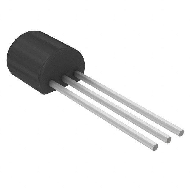
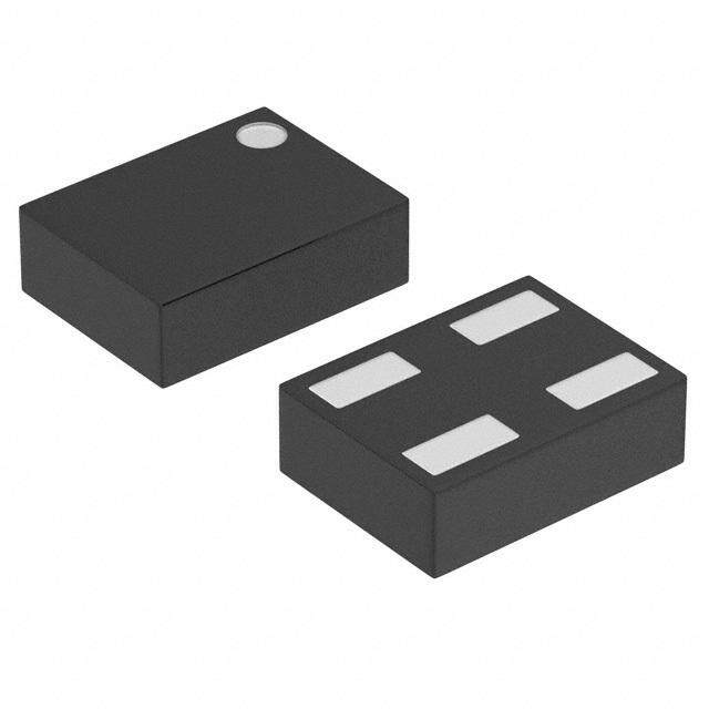
| 描述 | IC REG LDO ADJ 0.15A TSOT23-5低压差稳压器 Low Noise 150mA Adj |
| 产品分类 | |
| 品牌 | Vishay / SiliconixVishay Siliconix |
| 产品手册 | |
| 产品图片 |
|
| rohs | 符合RoHS无铅 / 符合限制有害物质指令(RoHS)规范要求 |
| 产品系列 | 电源管理 IC,低压差稳压器,Vishay / Siliconix SIP21108DT-T1-E3- |
| 数据手册 | |
| 产品型号 | SIP21108DT-T1-E3SIP21108DT-T1-E3 |
| 产品目录页面 | |
| 产品种类 | 低压差稳压器 |
| 供应商器件封装 | TSOT-23-5 |
| 其它名称 | SIP21108DT-T1-E3TR |
| 包装 | 带卷 (TR) |
| 商标 | Vishay / Siliconix |
| 安装类型 | 表面贴装 |
| 安装风格 | SMD/SMT |
| 封装 | Reel |
| 封装/外壳 | SOT-23-5 细型,TSOT-23-5 |
| 封装/箱体 | SOT-23 |
| 工作温度 | -40°C ~ 85°C |
| 工厂包装数量 | 3000 |
| 最大功率耗散 | 0.305 W |
| 最大工作温度 | + 85 C |
| 最大输入电压 | 6 V |
| 最小工作温度 | - 40 C |
| 最小输入电压 | + 2.2 V |
| 标准包装 | 3,000 |
| 电压-跌落(典型值) | 0.16V @ 150mA |
| 电压-输入 | 2.2 V ~ 6 V |
| 电压-输出 | 可调 |
| 电流-输出 | 150mA |
| 电流-限制(最小值) | 170mA |
| 稳压器拓扑 | 正,可调式 |
| 稳压器数 | 1 |
| 系列 | SIP2110x |
| 线路调整率 | 0.2 % / V |
| 输出电流 | 150 mA |
| 输出端数量 | 1 Output |
| 输出类型 | Adjustable |
| 零件号别名 | SIP21108DT-E3 |


- 商务部:美国ITC正式对集成电路等产品启动337调查
- 曝三星4nm工艺存在良率问题 高通将骁龙8 Gen1或转产台积电
- 太阳诱电将投资9.5亿元在常州建新厂生产MLCC 预计2023年完工
- 英特尔发布欧洲新工厂建设计划 深化IDM 2.0 战略
- 台积电先进制程称霸业界 有大客户加持明年业绩稳了
- 达到5530亿美元!SIA预计今年全球半导体销售额将创下新高
- 英特尔拟将自动驾驶子公司Mobileye上市 估值或超500亿美元
- 三星加码芯片和SET,合并消费电子和移动部门,撤换高东真等 CEO
- 三星电子宣布重大人事变动 还合并消费电子和移动部门
- 海关总署:前11个月进口集成电路产品价值2.52万亿元 增长14.8%


PDF Datasheet 数据手册内容提取
End of Life. Last Available Purchase Date is 31-Dec-2014 SiP21106, SiP21107, SiP21108 Vishay Siliconix 150-mA Low Noise, Low Dropout Regulator DESCRIPTION FEATURES The SiP21106 BiCMOS 150 mA low noise LDO voltage (cid:129) SC70-5L (2.1 mm x 2.1 mm x 0.95 mm) regulators are the perfect choice for low battery operated low (cid:129) TSOT23-5L (3.05 mm x 2.85 mm x 1.0 mm) powered applications. An ultra low ground current and low (cid:129) TSC75-6L package (1.6 mm x 1.6 mm RoHS dropout voltage of 135 mV at 150 mA load helps to extend x 0.55 mm), TSOT23-5L and SC70-5L COMPLIANT battery life for portable electronics. Systems requiring a quiet Package Options voltage source, such as RF applications, will benefit from the (cid:129) 1.0 % output voltage accuracy at 25 °C SiP21106 low output noise. (cid:129) Low dropout voltage: 135 mV at 150 mA The SiP21107 do not require a noise bypass capacitor and (cid:129) SiP21106 low noise: 60 µV (10 Hz to 100 kHz provides an error flag pin (POK or Power OK). POK output (rms) bandwidth) with 10 nF over full load range requires an external pull-up resistor and goes low when the (cid:129) 35 µA (typical) ground current at 1 mA load supply has not come up to voltage. (cid:129) 1 µA maximum shutdown current at 85 °C The SiP21108 output is adjusted with an external resistor network. (cid:129) Output auto discharge at shutdown mode The SiP21106, SiP21107, SiP21108 regulators allow stable (cid:129) Built-in short circuit (330 mA typical) and thermal operation with very small ceramic output capacitors, protection (160 °C typical) reducing board space and component cost. They are (cid:129) SiP21108 adjustable output voltage designed to maintain regulation while delivering 330 mA (cid:129) SiP21107 POK Error Flag peak current upon turn-on. During start-up, an active (cid:129) - 40 °C to + 125 °C junction temperature range for pull-down circuit improves the output transient response and operation regulation. In shutdown mode, the output automatically (cid:129) Uses low ESR ceramic capacitors discharges to ground through a 100 NMOS. (cid:129) Fixed voltage output 1.2 V to 5 V in 50 mV steps The SiP21106, SiP21107, SiP21108 are available in (cid:129) Compliant to RoHS Directive 2002/95/EC TSOT23-5L a super thin lead (Pb)-free TSC75-6L and SC70-5L packages for operation over the industrial operation APPLICATIONS range (- 40 °C to 85 °C). (cid:129) Cellular phones, wireless handsets (cid:129) PDAs (cid:129) MP3 players (cid:129) Digital cameras (cid:129) Pagers (cid:129) Wireless modem (cid:129) Noise-sensitive electronic systems TYPICAL APPLICATION CIRCUIT VIN 1 VIN VOUT 5 VOUT EN EN BP CIN= 1 µF COUT= 1 µF CBypass= 10 nF 2 GND GND NC SiP21106 SiP21106 EN 3 EN BP 4 VIN VIN VOUT VOUT CBypass= 10 nF CIN= 1 µF COUT= 1 µF TSOT23-5L/SC70-5LPackage TSC75-6L Package Document Number: 74442 www.vishay.com S09-1047-Rev. G, 08-Jun-09 1
End of Life. Last Available Purchase Date is 31-Dec-2014 SiP21106, SiP21107, SiP21108 Vishay Siliconix TYPICAL APPLICATION CIRCUIT 1 VIN VOUT 5 VOUT EN EN POK POK CIN= 1 µF COUT= 1 µF 2 GND GND NC SiP21107 SiP21107 3 EN POK 4 POK VIN VIN VOUT VOUT CIN= 1 µF COUT=1 µF TSOT23-5L/SC70-5LPackage TSC75L-6 Package VIN 1 VIN VOUT 5 VOUT EN EN Adj CIN= 1 µF 2 GND COUT= 1 µF GND NC SiP21108 SiP21108 EN 3 EN Adj 4 VIN VIN VOUT VOUT CIN= 1 µF COUT= 1 µF TSOT23-5L/SC70-5L Package TSC75-6L Package ABSOLUTE MAXIMUM RATINGS Parameter Limit Unit Input Voltage, V to GND - 0.3 to 6.5 IN V V (See Detailed Description) - 0.3 to 6.5 EN Output Current (I ) Short Circuit Protected OUT Output Voltage (V ) - 0.3 to V + 0.3 V OUT IN TSC75-6L TSOT23-5L SC70-5L Package Power Dissipation (P )a 420 305 187 mW D Package Thermal Resistance ( )b 131 180 294 °C/W JA Maximum Junction Temperature, T 125 J(max) Storage Temperature, T - 65 to 150 °C STG Lead Temperature, T c 260 L Notes: a. Derate 7.6 mW/°C for TSC75-6L package, 5.5 mW/°C for TSOT23-5L and 3.4 mW/°C for SC70-5L package above T = 70 °C. A b. Device mounted with all leads soldered or welded to multilayer 1S2P PC board. c. Soldering for 5 s. Stresses beyond those listed under "Absolute Maximum Ratings" may cause permanent damage to the device. These are stress ratings only, and functional operation of the device at these or any other conditions beyond those indicated in the operational sections of the specifications is not implied. Exposure to absolute maximum rating/conditions for extended periods may affect device reliability. RECOMMENDED OPERATING RANGE Parameter Limit Unit Input Voltage, V 2.2 to 6 V IN Operating Ambient Temperature T - 40 to 85 °C A www.vishay.com Document Number: 74442 2 S09-1047-Rev. G, 08-Jun-09
End of Life. Last Available Purchase Date is 31-Dec-2014 SiP21106, SiP21107, SiP21108 Vishay Siliconix SPECIFICATIONS Test Conditions Unless Specified V = V + 1.0 V = V IN OUT(nom) EN I = 1 mA, C = 1 µF, C = 1 µF OUT IN OUT Parameter Symbol - 40 °C < TA < 85 °C for full Temp.a Min.b Typ.c Max.b Unit Input Voltage Range V Full 2.2 6 V IN Room - 1.0 1.0 I = 1 mA OUT Full - 2.5 2.5 Output Voltage Accuracy V % OUT Room - 1.5 1.5 SiP21106/7 (1.2 V) I = 1 mA OUT Full - 4 4 Feedback Voltage Room 1.188 1.2 1.212 V V (SiP21108 Version only) Adj Full 1.170 1.230 Line Regulation LNR Full - 0.2 0.006 0.2 %/V V 2.6 V, OUT Room 0.003 0.006 I : 1 mA to 150 mA Load Regulation LDR OUTV < 2.6 V, %/mA OUT Room 0.005 0.009 I : 1 mA to 150 mA OUT Room 35 75 I = 1 mA OUT Full 85 Ground Pin Currente IGND Room 39 75 µA I = 150 mA OUT Full 85 Shutdown Supply Current ICC(off) VEN = 0 V Full 0.02 1 µA SiP21106 V = 2.8 V, BW = 10 Hz to 100 kHz, Room 60 OUT(nom) 1 mA < I < 150 mA, C = 0.01 µF Output Noise Voltagef (RMS) e OUT BP µV N SiP21107/8 V = 2.8 V, BW = 10 Hz to 100 kHz, Room 350 OUT(nom) 1 mA < I < 150 mA OUT Output Voltage Turn-On Time ton EN to VOUT delay; IOUT = 1 mA 70 µs f = 1 kHz Room 75 SiP21106, C = 0.01 µF BP f = 10 kHz Room 56 I = 10 mA OUT f = 100 kHz Room 40 Ripple Rejection PSRR dB SiP21107/8 f = 1 kHz Room 72 SiP21106, C = 0 µF f = 10 kHz Room 53 BP IOUT = 10 mA f = 100 kHz Room 38 Output Current Limit IO_LIM VOUT = 0 V Room 170 330 600 mA EN = 0 V, V = 1 V Room 100 OUT Auto Discharge Resistance R DIS For V < 2.2 V, EN = 0 V, V = 1 V Room 120 OUT OUT Room 45 I = 50 mA OUT Full 55 Dropout Voltaged Room 90 V I = 100 mA (2.2 V VOUT(nom) < 2.6 V) DO OUT Full 106 Room 135 250 I = 150 mA OUT Full 160 300 mV Room 45 I = 50 mA OUT Full 55 Dropout Voltage Room 90 V I = 100 mA (VOUT(nom) 2.6 V) DO OUT Full 106 Room 135 180 I = 150 mA OUT Full 160 220 V High = Regulator On (Rising) Full 1.2 ENH EN Pin Input Voltage V VENL Low = Regulator Off (Falling) Full 0.4 EN Pin Input Current I Room 0.009 µA EN Document Number: 74442 www.vishay.com S09-1047-Rev. G, 08-Jun-09 3
End of Life. Last Available Purchase Date is 31-Dec-2014 SiP21106, SiP21107, SiP21108 Vishay Siliconix SPECIFICATIONS Test Conditions Unless Specified V = V + 1.0 V IN OUT(nom) I = 1 mA, C = 1 µF, C = 1 µF OUT IN OUT Parameter Symbol - 40 °C < TA < 85 °C for full Temp.a Min.b Typ.c Max.b Unit Thermal Shutdown Junction Temperature T Room 160 J(S/D) °C Thermal Hysteresis T Room 20 HYST Error Flag Section (SiP21107 Version only) POK(OFF) Leakage IOFF RPU to VOUT or VIN Full 1 µA POK(ON) Voltage VPOKL EN = 0 V, IPOK = 0.5 mA Full 0.4 V V rising, POK goes high OUT 90 93 96 V 2.2 V, I = 1 mA POK Thresholdg V OUT(nom) OUT Full POKLH VOUT rising, POK goes high % 91 V < 2.2 V, I = 1 mA OUT(nom) OUT POK Hysteresis VHYST VIN falling, IOUT = 1 mA, POK goes low Room 1.5 POK Voltage Delay Time TP_Delay VOUT to POK delay, IOUT = 1 mA 40 µs Notes: a. Room = 25 °C, Full = - 40 to 85 °C. Derate 7.6 mW/°C for TSC75 and 5.5 mW/°C for SOT23 above T = 70 °C. A b. The algebraic convention whereby the most negative value is a minimum and the most positive a maximum. c. Typical values are for DESIGN AID ONLY, not guaranteed nor subject to production testing. d. Dropout voltage is defined as the input-to-output differential voltage at which the output voltage drops 2 % below its nominal value with constant load. For outputs = 2.2 V, dropout voltage is not applicable due to 2.2 V minimum input voltage requirement. e. Ground current is specified for normal operation as well as “drop-out” operation. f. Output noise is proportional to output voltage. Use formula e = 60 µV(rms)*V /2.8 V. N OUT g. POK threshold percentage is calculated by V /V x 100 %. The POK is measured with a differential voltage across V and V until POK IN OUT IN OUT turn on (low threshold) or off (high threshold). For V less than 2.2 V, POK is guaranteed functionality only. OUT TIMING WAVEFORMS VIN VEN tr 1 µs 0 V tON VNOM 0.95 VNOM VOUT Figure 1. www.vishay.com Document Number: 74442 4 S09-1047-Rev. G, 08-Jun-09
End of Life. Last Available Purchase Date is 31-Dec-2014 SiP21106, SiP21107, SiP21108 Vishay Siliconix PIN CONFIGURATION EN BP/Adj/POK BP/Adj/POK EN 6 1 GND NC NC 5 2 GND 4 3 VIN VOUT VOUT VIN TOP VIEW TSC75-6L Package (1.6 mm x 1.6 mm x 0.55 mm) BOTTOM VIEW VIN 1 5 VOUT VOUT 5 1 VIN GND 2 2 GND EN 3 4 BP/Adj/POK BP/Adj/POK 4 3 EN TOP VIEW BOTTOM VIEW TSOT23-5L/SC70-5LPackage Figure 2. PIN DESCRIPTION Pin Number Pin Number TSC75-6L TSOT23-5L/ Name Function SC70-5L By applying less than 0.4 V to this pin, the device will be turned off. Connect this pin to 1 3 EN V if unused. Do not leave floating. IN 2 2 GND Ground pin. For better thermal capability, directly connected to large ground plane. 3 1 VIN Input supply pin. Bypass this pin with a 1 µF ceramic or tantalum capacitor to ground. 4 5 VOUT Output voltage. Connect COUT between this pin and ground. 5 - NC No Connection. - BP (SiP21106): Noise bypass pin. For low noise applications, a 10 nF ceramic capacitor should be connected from this pin to ground. - Adj (SiP21108): Adjust input pin. Connect feedback resistors to program the output voltage for trim value of 1.2005 V. 6 4 BP/Adj/POK - POK (SiP21107): Power OK (error flag) pin. Open-drain output, which requires connecting a pull-up resistor to V or V . POK pin is actively high to indicate an output IN OUT normal operation condition on regulator and goes low to indicate under-voltage fault condition. Document Number: 74442 www.vishay.com S09-1047-Rev. G, 08-Jun-09 5
End of Life. Last Available Purchase Date is 31-Dec-2014 SiP21106, SiP21107, SiP21108 Vishay Siliconix ORDERING INFORMATION Part Number Marking Voltage Temperature Range Package SiP21108DVP-T1-E3 AA Adjustable SiP21106DVP-12-E3 BA 1.2 SiP21106DVP-18-E3 BG 1.8 SiP21106DVP-25-E3 BP 2.5 SiP21106DVP-26-E3 BR 2.6 SiP21106DVP-28-E3 BT 2.8 SiP21106DVP-285-E3 CT 2.85 SiP21106DVP-30-E3 BV 3 SiP21106DVP-33-E3 BY 3.3 SiP21106DVP-46-E3 CM 4.6 - 40 °C to 85 °C TSC75-6L SiP21106DVP-475-E3 CU 4.75 SiP21107DVP-12-E3 DA 1.2 SiP21107DVP-18-E3 DG 1.8 SiP21107DVP-25-E3 DP 2.5 SiP21107DVP-26-E3 DR 2.6 SiP21107DVP-28-E3 DT 2.8 SiP21107DVP-30-E3 DV 3 SiP21107DVP-33-E3 DY 3.3 SiP21107DVP-46-E3 EM 4.6 SiP21107DVP-285-E3 ET 2.85 SiP21108DT-T1-E3 N9 Adjustable SiP21106DT-12-E3 NP 1.2 SiP21106DT-18-E3 N1 1.8 SiP21106DT-25-E3 NA 2.5 SiP21106DT-26-E3 NC 2.6 SiP21106DT-28-E3 N2 2.8 SiP21106DT-285-E3 NE 2.85 SiP21106DT-30-E3 NG 3 SiP21106DT-33-E3 N3 3.3 SiP21106DT-45-E3 NM 4.5 SiP21106DT-46-E3 N4 4.6 - 40 °C to 85 °C TSOT23-5L SiP21106DT-475-E3 NJ 4.75 SiP21107DT-12-E3 NQ 1.2 SiP21107DT-18-E3 N5 1.8 SiP21107DT-25-E3 NB 2.5 SiP21107DT-26-E3 ND 2.6 SiP21107DT-28-E3 N6 2.8 SiP21107DT-285-E3 NF 2.85 SiP21107DT-30-E3 NH 3 SiP21107DT-33-E3 N7 3.3 SiP21107DT-46-E3 N8 4.6 www.vishay.com Document Number: 74442 6 S09-1047-Rev. G, 08-Jun-09
End of Life. Last Available Purchase Date is 31-Dec-2014 SiP21106, SiP21107, SiP21108 Vishay Siliconix ORDERING INFORMATION SiP21108DR-T1-E3 N9 Adjustable SiP21106DR-12-E3 NP 1.2 SiP21106DR-18-E3 N1 1.8 SiP21106DR-25-E3 NA 2.5 SiP21106DR-26-E3 NC 2.6 SiP21106DR-28-E3 N2 2.8 SiP21106DR-285-E3 NE 2.85 SiP21106DR-30-E3 NG 3 SiP21106DR-33-E3 N3 3.3 SiP21106DR-46-E3 N4 4.6 - 40 °C to 85 °C SC70-5L SiP21106DR-475-E3 NJ 4.75 SiP21107DR-12-E3 NQ 1.2 SiP21107DR-18-E3 N5 1.8 SiP21107DR-25-E3 NB 2.5 SiP21107DR-26-E3 ND 2.6 SiP21107DR-28-E3 N6 2.8 SiP21107DR-285-E3 NF 2.85 SiP21107DR-30-E3 NH 3 SiP21107DR-33-E3 N7 3.3 SiP21107DR-46-E3 N8 4.6 Note: Other fixed output voltage options are available. Please contact your Vishay sales representative or distributor for details. Document Number: 74442 www.vishay.com S09-1047-Rev. G, 08-Jun-09 7
End of Life. Last Available Purchase Date is 31-Dec-2014 SiP21106, SiP21107, SiP21108 Vishay Siliconix TYPICAL CHARACTERISTICS 3.0 1.00 2.5 0.50 2.0 (V)T 1.5 IOUT = 0 mA on (%) 0.00 IOUT = 1 mA VOU IOUT = 150 mA eviati - 0.50 D 1.0 - 1.00 0.5 SiP21106: 2.8 V SiP21106: 2.8 V 0.0 - 1.50 0 1 2 3 4 5 6 - 40 - 15 10 35 60 85 VIN (V) Temperature (°C) Output Voltage vs. Input Voltage Output Voltage Accuracy vs. Temperature 180 180 SiP21106: 2.8 V 160 160 140 TA = + 85 °C IOUT = 150 mA 120 140 TA = + 25 °C mV) 100 mV) V (DO 80 V (DO 120 60 100 IOUT = 100 mA 40 TA = - 40 °C 80 20 SiP21106: 2.8 V 0 60 0 25 50 75 100 125 150 2.0 2.5 3.0 3.5 4.0 4.5 5.0 5.5 6.0 IOUT(mA) VIN (V) Dropout Voltage vs. Load Current Dropout Voltage vs. Input Voltage 180 41 160 40 IOUT = 150 mA IOUT = 150 mA 140 39 120 V) 38 (m 100 IOUT = 100 mA O D 37 V 80 36 IOUT = 1 mA 60 IOUT = 50 mA 35 40 SiP21106: 2.8 V SiP21106: 2.8 V 20 34 - 40 - 15 10 35 60 85 - 40 - 15 10 35 60 85 Temperature (°C) Temperature (°C) Dropout Voltage vs. Temperature Ground Current vs. Temperature www.vishay.com Document Number: 74442 8 S09-1047-Rev. G, 08-Jun-09
End of Life. Last Available Purchase Date is 31-Dec-2014 SiP21106, SiP21107, SiP21108 Vishay Siliconix TYPICAL CHARACTERISTICS 50 50 VIN = 5.5 V IOUT = 150 mA 45 40 VIN = 3.8 V µA) 40 A) 30 IOUT = 1 mA (D (µD IGN35 IGN 20 30 10 SiP21106: 2.8 V SiP21106: 2.8 V 25 0 0 25 50 75 100 125 150 0 1 2 3 4 5 6 IOUT (mA) VIN (V) Ground Current vs. Output Current Ground Current vs. Input Voltage at 25 °C 80 2.820 SiP21106 SiP21106: 2.8 V 70 CBP= 10 nF VIN= 3.8 V 60 IOUT= 10 mA 2.800 IOUT= 1 mA 50 dB) V) 2.780 R ( 40 ( PSR 30 VOUT 2.760 IOUT= 50 mA 20 IOUT= 150 mA 2.740 10 0 10 100 1000 10 000 100 000 1 000 000 2.720 - 40 - 15 10 35 60 85 Frequency (Hz) Temperature (°C) PSRR Output Voltage Accuracy vs. Load Current 400 SiP21106: 2.8 V 350 300 V) µ e ( 250 s oi N ut 200 p ut O 150 100 50 0 0.001 0.0056 0.01 0.056 0.1 BP Capacitance (µF) Output Noise vs. BP Capacitance Document Number: 74442 www.vishay.com S09-1047-Rev. G, 08-Jun-09 9
End of Life. Last Available Purchase Date is 31-Dec-2014 SiP21106, SiP21107, SiP21108 Vishay Siliconix TYPICAL OPERATING WAVEFORMS IOUT (100 mA/DIV) IOUT (100 mA/DIV) VOUT (50 mV/DIV) VOUT (50 mV/DIV) SiP21106: 2.8 V SiP21106: 4.6 V VVCCCIOIOBNNUPU == TT= 5=1= 1. 54µ01 . FV6nµ FFV VVCCCIOIOBNNUPU == TT= 3=1= 1. 8µ201 . FV8nµ FFV 50 µs/DIV 50 µs/DIV Load Transient Response Load Transient Response SiP21106: 4.6 V SiP21106: 2.8 V VIN = 5.0 to 5.5 V VIN = 3.8 to 4.8 V VOUT = 4.6 V VOUT = 2.8 V IOUT = 150 mA IOUT = 150 mA CIN = 1 µF CIN = 1 µF COUT = 1 µF COUT = 1 µF CBP = 10 nF CBP = 10 nF VIN (1 V/DIV) AC Coupling AC Coupling VIN (200 mV/DIV) VOUT (10 mV/DIV) VOUT (10 mV/DIV) 200 µs/DIV 200 µs/DIV Line Transient Response Line Transient Response SiP21106: 4.6 V SiP21106: 2.8 V VIN = 5.0 to 5.5 V VIN = 3.8 to 4.8 V VOUT = 4.6 V VOUT = 2.8 V IOUT = 1 mA IOUT = 1 mA CIN = 1 µF CIN = 1 µF COUT = 1 µF COUT = 1 µF CBP = 10 nF CBP = 10 nF VIN (1 V/DIV) AC Coupling AC Coupling VIN (200 mV/DIV) VOUT (10 mV/DIV) VOUT (10 mV/DIV) 200 µs/DIV 200 µs/DIV Line Transient Response Line Transient Response www.vishay.com Document Number: 74442 10 S09-1047-Rev. G, 08-Jun-09
End of Life. Last Available Purchase Date is 31-Dec-2014 SiP21106, SiP21107, SiP21108 Vishay Siliconix TYPICAL OPERATING WAVEFORMS SiP21106: 2.8 V SiP21106: 2.8 V VVCCIOIONNUU ==TT 3=1=. 8µ21 .F V8µ FV VVCCCIOIOBNNUPU == TT= 3=1= 1. 8µ201 . FV8nµ FFV CBP = 10 nF IOUT (100 mA/DIV) IOUT (50 mA/DIV) 50 ms/DIV 50 ms/DIV Output Short Circuit Current Output Short Thermal Cycling SiP21106: 2.8 V SiP21106: 2.8 V VIN = 3.8 V VIN = 3.8 V VOUT = 2.8 V VOUT = 2.8 V CIN = 1 µF CCIONU =T 1= µ1 FµF VEN (500 mV/DIV) CCOBPU T= = 1 01 nµFF CBP = 10 nF VEN (1 V/DIV) IOUT = 150 mA IOUT = 150 mA VOUT (500 mV/DIV) VOUT (500 mV/DIV) 20 µs/DIV 20 µs/DIV Output Voltage Power-Down Output Voltage Start-Up SiP21107: 1.8 V VIN = 2.8 V VOUT (500 mV/DIV) VOUT = 1.8 V CIN = 1 µF COUT = 1 µF VOUT (500 mV/DIV) CBP = 10 nF IOUT = 1 mA POK (1 V/DIV) SiP21107: 2.8 V POK (1 V/DIV) VIN = 3.8 V VOUT = 2.8 V CIN = 1 µF COUT = 1 µF CBP = 10 nF IOUT = 1 mA 20 ms/DIV 20 ms/DIV POK pin goes low to indicate output under-voltage POK pin goes low to indicate output under-voltage fault condition fault condition Document Number: 74442 www.vishay.com S09-1047-Rev. G, 08-Jun-09 11
End of Life. Last Available Purchase Date is 31-Dec-2014 SiP21106, SiP21107, SiP21108 Vishay Siliconix TYPICAL OPERATING WAVEFORMS SiP21107: 1.8 V VIN = 2.8 V VOUT (500 mV/DIV) VOUT = 1.8 V CIN = 1 µF CCOBPU T= = 1 01 nµFF VOUT (500 mV/DIV) IOUT = 1 mA SiP21107: 2.8 V V = 3.8 V POK (1 V/DIV) IN VOUT = 2.8 V CIN = 1 µF POK (1 V/DIV) COUT = 1 µF CBP = 10 nF IOUT = 1 mA 20 µs/DIV 20 µs/DIV POK pin is actively high to indicate an output normal POK pin is actively high to indicate an output normal operation condition on regular operation condition on regular TYPICAL WAVEFORMS 1 z) H √ V/ µ y ( sit n e D 0.1 al SiP21106: 2.8 V SiP21106: 2.8 V ectr VIN = 3.8 V VIN = 4.5 V Sp VOUT = 2.8 V CVIONU =T 1= µ2F.8 V oise CCOINU =T =1 1µ FµF VOUT (100 µV/DIV) CCOBPU T= = 1 01 nµFF N CIOBUPT == 11000 n mFA VNOISE = 60 µVRMS IOUT = 150 mA 0.01 10 100 1K 10K 1 0 0 K 1M 2 ms/DIV Frequency (Hz) Output Noise Output Noise Spectral Density FUNCTIONAL BLOCK DIAGRAM VIN EN Enable Error-Amp B *P / A *d*j / P *O**K Bandgap Reference Current Limit and VOUT Thermal + POK - 0.94 VOUT SiP21106: BP SiP21107: POK SiP21108: Adj *SiP21106: BP ***SiP21107: POK GND **SiP21108: Adj Figure 3. www.vishay.com Document Number: 74442 12 S09-1047-Rev. G, 08-Jun-09
End of Life. Last Available Purchase Date is 31-Dec-2014 SiP21106, SiP21107, SiP21108 Vishay Siliconix DETAILED DESCRIPTION VIN As shown in the block diagram, the circuit consists of a bandgap reference, error amplifier, P-channel pass 1.2 V Reference + transistor and an internal feedback resistor voltage divider, Error-Amp which is used to monitor and control the output voltage. - VOUT A constant 1.2 V bandgap reference voltage is applied to the non-inverting input of the error amplifier. The error amplifier compares this reference with the feedback voltage on its R1 inverting input and amplifies the difference. If the feedback voltage is lower than the reference voltage, the pass-transistor gate is pulled low. This increases the R2 PMOS's gate to source voltage and allows more current to pass through the transistor to the output which increases the output voltage. Conversely, if the feedback voltage is higher Figure 4. than the reference voltage, the pass transistor gate is pulled The SiP21108 has a user-adjustable output that can be set high, decreasing the gate-to-source voltage, thereby through the resistor feedback network consisting of R and 1 allowing less current to pass to the output and causing it to R . R range of 100K to 400K is recommended to be 2 2 drop. consistent with ground current specification. R can then be 1 determined by the following equation: Internal P-Channel Pass Transistor A 0.9 (typical) P-channel MOSFET is used as the pass R = R x ( V O U T - 1) transistor for the SiP21106, SiP21107, SiP21108 part series. 1 2 V ref The MOSFET transistor offers many advantages over the Where V is typically 1.2005 V. Use 1 % or better resistors more, formerly, common PNP pass transistor designs, which ref for better output voltage accuracy (see Figure 4). ultimately result in longer battery lifetime. The main disadvantage of PNP pass transistors is that they require a Current Limit certain base current to stay on, which significantly increases The SiP21106, SiP21107, SiP21108 include a current limit under heavy load conditions. In addition, during dropout, block which monitors the current passing through the pass when the pass transistor saturates, the PNP regulators transistor through a current mirror and controls the gate waste considerable current. In contrast, P-channel voltage of the MOSFET, limiting the output current to 330 mA MOSFETS require virtually zero-base drive and do not suffer (typical). This current limit feature allows for the output to be from the stated problems. These savings in base drive shorted to ground for an indefinite amount of time without current translate to lower quiescent current which is typical damaging the device. around 35 µA as shown in the Typical Characteristics. Thermal-Overload Protection Shutdown and Auto-Dischage/No-Discharge The thermal overload protection limits the total power Bringing the EN voltage low will place the part in shutdown dissipation and protects the device from being damaged. mode where the device output enters a high-impedance When the junction temperature exceeds T = 150 °C, the state and the quiescent current is reduced to below 1 µA, J device turns the P-channel pass transistor off allowing the reducing the drain on the battery in standby mode and device to cool down. Once the temperature drops by about increasing standby time. Connect EN pin to input for normal 20 °C, the thermal sensor turns the pass transistor on again operation. The output has an internal pull down to discharge and resumes normal operation. Consequently, a continuous the output to ground when the EN pin is low. The internal pull thermal overload condition will result in a pulsed output. It is down is a 100 typical resistor, which can discharge a 1 µF generally recommended to not exceed the junction in less than 1 ms. Refer to Typical Operating Waveforms for temperature rating of 125 °C for continuous operation. turn-off waveforms. Noise Reduction in SiP21106 Output Voltage Selection For the SiP21106, an external 10 nF bypass capacitor at BP The SiP21106 has fixed voltage outputs that are preset to pin is used to create a low pass filter for noise reduction. The voltages from 1.2 V to 4.6 V (see Ordering Information). startup time is fast, since a power-on circuit pre-charges the bypass capacitor. After the power-up sequence the pre-charge circuit is switched to standby mode in order to save current. It is therefore not recommended to use larger bypass capacitor values than 50 nF. When the circuit is used without a capacitor, stable operation is guaranteed. Document Number: 74442 www.vishay.com S09-1047-Rev. G, 08-Jun-09 13
End of Life. Last Available Purchase Date is 31-Dec-2014 SiP21106, SiP21107, SiP21108 Vishay Siliconix POK Status in SiP21107 The GND pin of the SiP2110 acts as both the electrical The POK comparator monitors the output until the supply connection to GND as well as a path for channeling away comes up to specified percentage of VIN. This open drain heat. Connect this pin to a GND plane to maximize heat NMOS output requires an external pull-up resistor to either dissipation. Once maximum power dissipation is calculated VOUT or VIN. The internal NMOS can drive up to 0.5 mA using the equation above, the maximum allowable output loads. POK pin is active high to indicate that output is within current for any input/output potential can be calculated as percentage tolerance. POK goes low when output is outside of this tolerance as when in dropout, over current and P thermal shutdown. IOUT(max) = (max) V - V IN OUT APPLICATION INFORMATION PCB Layout The component placement around the LDO should be done Input/Output Capacitor Selection and Regulator Stability carefully to achieve good dynamic line and load response. It is recommended that a low ESR 1 µF capacitor be used on The input and noise capacitor should be kept close to the the SiP21106, SiP21107, SiP21108 input. A larger input LDO. The rise in junction temperature depends on how capacitance with lower ESR would improve noise rejection efficiently the heat is carried away from junction-to-ambient. and line-transient response. A larger input bypass capacitor The junction-to-lead thermal impedance is a characteristic of may be required in applications involving long inductive the package and is fixed. The thermal impedance between traces between the source and LDO. The circuit is stable with lead-to-ambient can be reduced by increasing the copper only a small output capacitor equal to 6 nF/mA ( 1 µF at area on PCB. Increase the input, output and ground trace 150 mA) of load. Since the bandwidth of the error amplifier is area to reduce the junction-to-ambient thermal impedance. around 1 MHz - 3 MHz and the dominant pole is at the output node, the capacitor should be capacitive in this range, i.e., for 150 mA load current, an ESR < 0.4 is necessary. Parasitic inductance of about 10 nH can be tolerated. Applying a larger output capacitor would increase power supply rejection and improve load-transient response. Some ceramic dielectrics such as the Z5U and Y5V exhibit large capacitance and ESR variation over temperature. If such capacitors are used, a 2.2 µF or larger value may be needed to ensure stability over the industrial temperature range. If using higher quality ceramic capacitors, such as those with X7R and Y7R dielectrics, a 1 µF capacitor will be sufficient at all operating temperatures. Operating Region and Power Dissipation An important consideration when designing power supplies is the maximum allowable power dissipation of a part. The maximum power dissipation in any application is dependant on the maximum junction temperature, T = 125 °C, the J(max) ambient temperature, T , and the junction-to-ambient A thermal resistance for the package, which is the summation of , the thermal resistance of the package, and , the J-C C-A thermal resistance through the PC board and copper traces. Power dissipation may be expressed as: P(max) = TJ (max) - TA θ + θ J-C C-A Vishay Siliconix maintains worldwide manufacturing capability. Products may be manufactured at one of several qualified locations. Reliability data for Silicon Technology and Package Reliability represent a composite of all qualified locations. For related documents such as package/tape drawings, part marking, and reliability data, see www.vishay.com/ppg?74442. www.vishay.com Document Number: 74442 14 S09-1047-Rev. G, 08-Jun-09
Package Information www.vishay.com Vishay Siliconix Thin SOT-23 : 5- and 6-Lead (Power IC only) e1 6 5 4 E1 E 1 2 3 -B- 4 Pin #1 indetifier e 0.15 M C B A b -A- D 4x θ1 0.17 ref c R R A2 A L Gage plane Seating plane θ Seating plane 4 xθ1 0.08 C A1 L -C- (L1) Notes: 1. Use millimeters as the primary measurement. 2. Dimensioning and tolerances conform to ASME Y14.5M. - 1994. 3. This part is fully compliant with JEDEC MO-193. 4. Detail of Pin #1 indentifier is optional. MILLIMETERS INCHES DIM. MIN. NOM. MAX. MIN. NOM. MAX. A 0.91 1.00 1.10 0.036 0.039 0.043 A1 0.00 0.05 0.10 0.000 0.002 0.004 A2 0.85 0.90 1.00 0.033 0.035 0.039 b 0.30 0.40 0.45 0.012 0.016 0.018 c 0.10 0.15 0.20 0.004 0.006 0.008 D 2.85 2.95 3.10 0.112 0.116 0.122 E 2.70 2.85 2.98 0.106 0.112 0.117 E1 1.525 1.65 1.70 0.060 0.065 0.067 e 0.95 BSC 0.0374 BSC L 0.30 0.40 0.50 0.014 - 0.020 L1 0.60 ref. 0.024 BSC L2 0.25 BSC 0.010 BSC 0° 4° 8° 0° 4° 8° 1 4° 10° 12° 4° 10° 12° ECN: E13-1126-Rev. B, 01-Jul-13 DWG: 5926 Revision: 01-Jul-13 1 Document Number: 72821 For technical questions, contact: powerictechsupport@vishay.com THIS DOCUMENT IS SUBJECT TO CHANGE WITHOUT NOTICE. THE PRODUCTS DESCRIBED HEREIN AND THIS DOCUMENT ARE SUBJECT TO SPECIFIC DISCLAIMERS, SET FORTH AT www.vishay.com/doc?91000
Package Information Vishay Siliconix SC-70: 3/4/5/6-LEADS (PIC ONLY) D 0.15 (0.006) C e1 A A D N5 N4 N3 E/2 E1/2 E E/1 0.15 (0.006) C Pin 1 N1 N2 e B See Detail A C 0.10 (0.004) M C A B b U1 A2 A SEATING PLANE A1 C 0.10 (0.004) C H (b) b1 0.15 (0.0059) GAGE PLANE c1 c Base Metal U L SECTIION A-A DETAIL A LEAD COUNT PPiinn NOTES: Code 3 4 5 6 1. Dimensioning and tolerancing per ANSI Y14.5M-1994. N1 − − 2 2 2. Controlling dimensions: millimeters converted to inch dimensions are N2 2 2 3 3 not necessarily exact. N3 − 3 4 4 3. Dimension “D” does not include mold flash, protrusion or gate burr. Mold flash, protrusion or gate burr shall not exceed 0.15 mm N4 3 − − 5 (0.006 inch) per side. N5 − 4 5 6 4. The package top shall be smaller than the package bottom. Dimension “D” and “E1” are determined at the outer most extremes of the plastic body exclusive of mold flash, tie bar burrs, gate burrs and interlead flash, but including any mismatch between the top and bottom of the plastic body. Document Number: 73201 www.vishay.com 19-Nov-04 1
Package Information Vishay Siliconix MILLIMETERS INCHES Dim Min Nom Max Min Nom Max A 0.80 − 1.10 0.031 − 0.043 A1 0.00 − 0.10 0.000 − 0.004 A2 0.80 0.90 1.00 0.031 0.035 0.040 b 0.15 − 0.30 0.006 − 0.012 b1 0.15 0.20 0.25 0.006 0.008 0.010 c 0.08 − 0.25 0.003 − 0.010 c1 0.08 0.13 0.20 0.003 0.005 0.008 D 1.90 2.10 2.15 0.074 0.082 0.084 E 2.00 2.10 2.20 0.078 0.082 0.086 E1 1.15 1.25 1.35 0.045 0.050 0.055 e 0.65 BSC 0.0255 BSC e1 1.30 BSC 0.0512 BSC L 0.26 0.36 0.46 0.010 0.014 0.018 U 0(cid:1) − 8(cid:1) 0(cid:1) − 8(cid:1) U1 4(cid:1) 10(cid:1) 4(cid:1) 10(cid:1) ECN: S-42145—Rev. A, 22-Nov-04 DWG: 5941 www.vishay.com Document Number: 73201 2 19-Nov-04
Package Information Vishay Siliconix PowerPAK ® TSC75-6L (Power IC only) D1 Exposed pad e D b Pin4 Pin 5 Pin6 K PPAK TSC75 E1 E (1.6 x 1.6 mm) Exposed pad K L Pin3 Pin 2 Pin1 e1 K2 K2 Pin 1 Dot By Marking Top View Bottom View A C A1 Side View MILLIMETERS INCHES DIM Min Nom Max Min Nom Max A 0.50 0.55 0.65 0.020 0.022 0.026 A1 0 - 0.05 0 - 0.002 b 0.20 0.25 0.30 0.008 0.010 0.012 C 0.10 0.15 0.20 0.006 0.008 0.010 D 1.55 1.60 1.65 0.0061 0.063 0.065 D1 0.95 1.00 1.05 0.037 0.039 0.041 E 1.55 1.60 1.65 0.061 0.063 0.065 E1 0.55 0.60 0.65 0.022 0.024 0.026 e 0.50 BSC 0.020 BSC e1 1.00 BSC 0.039 BSC K 0.15 - - 0.006 - - K2 0.20 - - 0.008 L 0.20 0.25 0.30 0.008 0.010 0.012 ECN: S-61919-Rev. A, 02-Oct-06 DWG: 5955 Document Number: 74416 www.vishay.com 02-Oct-06 1
Legal Disclaimer Notice www.vishay.com Vishay Disclaimer ALL PRODUCT, PRODUCT SPECIFICATIONS AND DATA ARE SUBJECT TO CHANGE WITHOUT NOTICE TO IMPROV E RELIABILITY, FUNCTION OR DESIGN OR OTHERWISE. Vishay Intertechnology, Inc., its affiliates, agents, and employees, and all persons acting on its or their behalf (collectively, “Vishay”), disclaim any and all liability for any errors, inaccuracies or incompleteness contained in any datasheet or in any other disclosure relating to any product. Vishay makes no warranty, representation or guarantee regarding the suitability of the products for any particular purpose o r the continuing production of any product. To the maximum extent permitted by applicable law, Vishay disclaims (i) any and all liability arising out of the application or use of any product, (ii) any and all liability, including without limitation special, consequential or incidental damages, and (iii) any and all implied warranties, including warranties of fitness for particular purpose, non-infringement and merchantability. Statements regarding the suitability of products for certain types of applications are based on Vishay’s knowledge of typical requirements that are often placed on Vishay products in generic applications. Such statements are not binding statements about the suitability of products for a particular application. It is the customer’s responsibility to validate that a particular product with the properties described in the product specification is suitable for use in a particular application. Parameters provided in datasheets and / or specifications may vary in different applications and performance may vary over time. All operating parameters, including typical parameters, must be validated for each customer application by the customer’s technical experts. Product specifications do not expand or otherwise modify Vishay’s terms and conditions of purchase, including but not limited to the warranty expressed therein. Except as expressly indicated in writing, Vishay products are not designed for use in medical, life-saving, or life-sustainin g applications or for any other application in which the failure of the Vishay product could result in personal injury or death. Customers using or selling Vishay products not expressly indicated for use in such applications do so at their own risk . Please contact authorized Vishay personnel to obtain written terms and conditions regarding products designed for such applications. No license, express or implied, by estoppel or otherwise, to any intellectual property rights is granted by this documen t or by any conduct of Vishay. Product names and markings noted herein may be trademarks of their respective owners. © 2021 VISHAY INTERTECHNOLOGY, INC. ALL RIGHTS RESERVED Revision: 01-Jan-2021 1 Document Number: 91000