ICGOO在线商城 > 集成电路(IC) > PMIC - 稳压器 - 线性 > LM2990T-5.0/NOPB

 Datasheet下载
- 型号: LM2990T-5.0/NOPB
- 制造商: Texas Instruments
- 库位|库存: xxxx|xxxx
- 要求:
| 数量阶梯 | 香港交货 | 国内含税 |
| +xxxx | $xxxx | ¥xxxx |
查看当月历史价格
查看今年历史价格
LM2990T-5.0/NOPB产品简介:
ICGOO电子元器件商城为您提供LM2990T-5.0/NOPB由Texas Instruments设计生产,在icgoo商城现货销售,并且可以通过原厂、代理商等渠道进行代购。 LM2990T-5.0/NOPB价格参考¥10.24-¥20.98。Texas InstrumentsLM2990T-5.0/NOPB封装/规格:PMIC - 稳压器 - 线性, Linear Voltage Regulator IC Negative Fixed 1 Output -5V 1.8A TO-220-3。您可以下载LM2990T-5.0/NOPB参考资料、Datasheet数据手册功能说明书,资料中有LM2990T-5.0/NOPB 详细功能的应用电路图电压和使用方法及教程。
LM2990T-5.0/NOPB 是由德州仪器(Texas Instruments)制造的一款线性稳压器,属于PMIC(电源管理集成电路)类别。它具有低功耗、低压差(Low Dropout, LDO)特性,广泛应用于需要稳定5V输出电压的场合。

 应用场景

1. 便携式电子设备:
   - LM2990T-5.0/NOPB 适用于各种便携式电子设备,如手机、平板电脑、便携式音频播放器等。这些设备通常依赖电池供电,要求电源管理芯片具备高效能和低功耗特性,以延长电池寿命。

2. 嵌入式系统:
   - 在嵌入式系统中,如单片机(MCU)、微控制器模块等,该稳压器可以为系统提供稳定的5V电源。其低压差特性使其能够在输入电压较低的情况下保持输出电压的稳定性,特别适合电池供电的应用。

3. 传感器与数据采集系统:
   - 传感器和数据采集系统需要高精度的电源供应,以确保测量结果的准确性。LM2990T-5.0/NOPB 提供的稳定5V输出能够满足这些应用的需求,同时其低噪声特性有助于提高系统的信号完整性。

4. 工业控制与自动化:
   - 在工业环境中,许多设备和模块需要稳定的电源供应。例如,PLC(可编程逻辑控制器)、人机界面(HMI)、通信模块等都可以使用该稳压器来确保电源的稳定性,从而提高整个系统的可靠性。

5. 医疗设备:
   - 医疗设备对电源的要求非常严格,必须保证电源的稳定性和安全性。LM2990T-5.0/NOPB 可以为便携式医疗设备(如血糖仪、心率监测仪等)提供可靠的5V电源,确保设备正常工作。

6. 消费电子产品:
   - 在消费电子产品中,如数码相机、电子书阅读器等,该稳压器可以为内部电路提供稳定的电源,确保设备在不同工作模式下的性能一致。

总之,LM2990T-5.0/NOPB 凭借其低功耗、低压差和高稳定性等特点,适用于多种需要5V稳定电源的应用场景,尤其适合电池供电和对电源质量要求较高的设备。
| 参数 | 数值 |
| 产品目录 | 集成电路 (IC)半导体 |
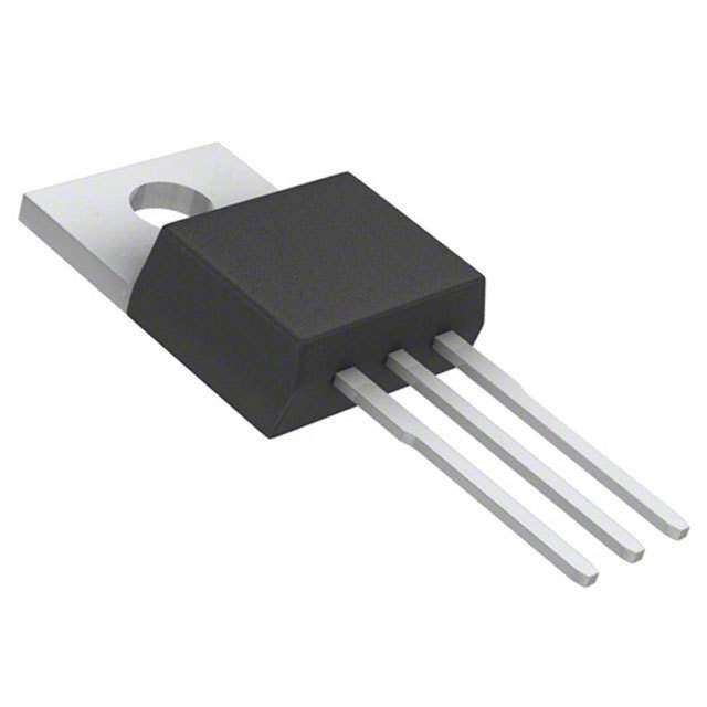
| 描述 | IC REG LDO -5V 1.8A TO220-3低压差稳压器 NEG LDO REG |
| 产品分类 | |
| 品牌 | Texas Instruments |
| 产品手册 | |
| 产品图片 |
|
| rohs | 符合RoHS含铅 / 不受限制有害物质指令(RoHS)规范要求限制 |
| 产品系列 | 电源管理 IC,低压差稳压器,Texas Instruments LM2990T-5.0/NOPB- |
| 数据手册 | |
| 产品型号 | LM2990T-5.0/NOPB |
| 产品目录页面 | |
| 产品种类 | 低压差稳压器 |
| 供应商器件封装 | TO-220-3 |
| 其它名称 | *LM2990T-5.0/NOPB |
| 制造商产品页 | http://www.ti.com/general/docs/suppproductinfo.tsp?distId=10&orderablePartNumber=LM2990T-5.0/NOPB |
| 包装 | 管件 |
| 商标 | Texas Instruments |
| 回动电压—最大值 | 600 mV |
| 安装类型 | 通孔 |
| 安装风格 | Through Hole |
| 封装 | Tube |
| 封装/外壳 | TO-220-3 |
| 封装/箱体 | TO-220-3 |
| 工作温度 | -40°C ~ 125°C |
| 工厂包装数量 | 45 |
| 最大输入电压 | - 26 V |
| 标准包装 | 45 |
| 电压-跌落(典型值) | 0.6V @ 1A |
| 电压-输入 | 可下调至 -26V |
| 电压-输出 | -5V |
| 电流-输出 | 1.8A |
| 电流-限制(最小值) | - |
| 稳压器拓扑 | 负,固定式 |
| 稳压器数 | 1 |
| 系列 | LM2990 |
| 设计资源 | http://www.digikey.com/product-highlights/cn/zh/texas-instruments-webench-design-center/3176 |
| 输出电流 | 1.5 A |


- 商务部:美国ITC正式对集成电路等产品启动337调查
- 曝三星4nm工艺存在良率问题 高通将骁龙8 Gen1或转产台积电
- 太阳诱电将投资9.5亿元在常州建新厂生产MLCC 预计2023年完工
- 英特尔发布欧洲新工厂建设计划 深化IDM 2.0 战略
- 台积电先进制程称霸业界 有大客户加持明年业绩稳了
- 达到5530亿美元!SIA预计今年全球半导体销售额将创下新高
- 英特尔拟将自动驾驶子公司Mobileye上市 估值或超500亿美元
- 三星加码芯片和SET,合并消费电子和移动部门,撤换高东真等 CEO
- 三星电子宣布重大人事变动 还合并消费电子和移动部门
- 海关总署:前11个月进口集成电路产品价值2.52万亿元 增长14.8%


PDF Datasheet 数据手册内容提取
Product Sample & Technical Tools & Support & Folder Buy Documents Software Community LM2990 SNVS093G–JUNE1999–REVISEDMAY2015 LM2990 Negative Low-Dropout Regulator 1 Features 3 Description • InputVoltage: –26Vto –6V The LM2990 is a three-terminal, low-dropout, 1-A 1 negative voltage regulator available with fixed output • FixedOutputVoltages: −5V, −5.2V, −12V,and voltagesof−5V, −5.2V, −12V,and −15V. −15V The LM2990 uses circuit design techniques to • 5%OutputAccuracyoverEntireOperatingRange provide low-dropout and low-quiescent current. The • OutputCurrentinExcessof1A dropout voltage at 1-A load current is typically 0.6 V • DropoutVoltageTypically0.6Vat1-ALoad and an ensured worst-case maximum of 1 V over the entire operating temperature range. The quiescent • LowQuiescentCurrent current is typically 1 mA with 1-A load current and an • InternalShort-CircuitCurrentLimit input-output voltage differential greater than 3 V. A • InternalThermalShutdownwithHysteresis unique circuit design of the internal bias supply limits • FunctionalComplementtotheLM2940Series the quiescent current to only 9 mA (typical) when the regulator is in the dropout mode (V − V ≤ 3 V). OUT IN 2 Applications Output voltage accuracy is ensured to ±5% over load andtemperatureextremes. • PostSwitcherRegulator The LM2990 also implements short-circuit proof, and • Local,On-CardRegulation thermal shutdown includes hysteresis to enhance the • BatteryOperatedEquipment reliability of the device when overloaded for an space extendedperiodoftime. space All these features make the LM2990 an ideal space negative power supply suited for dual supply systems. The device may also be used as fixed or TypicalApplication adjustablecurrentsinkload. TheLM2990isavailableintwo3-pinpackagesandis rated for operation over the junction temperature rangeof−40°Cto125°C. DeviceInformation(1) *and**:Requiredforstability.Mustbeat PARTNUMBER PACKAGE BODYSIZE(NOM) leasta10-μFaluminumelectrolyticora1- DDPAK/TO-263(3) 10.20mmx9.00mm μFsolidtantalumtomaintainstability.May LM2990 beincreasedwithoutboundtomaintain TO-220(3) 14.99mmx10.16mm regulationduringtransients.Locatethe (1) For all available packages, see the orderable addendum at capacitorascloseaspossibletothe theendofthedatasheet. regulator.Theequivalentseriesresistance (ESR)iscritical,andshouldbelessthan 10Ωoverthesameoperatingtemperature rangeastheregulator. 1 An IMPORTANT NOTICE at the end of this data sheet addresses availability, warranty, changes, use in safety-critical applications, intellectualpropertymattersandotherimportantdisclaimers.PRODUCTIONDATA.
LM2990 SNVS093G–JUNE1999–REVISEDMAY2015 www.ti.com Table of Contents 1 Features.................................................................. 1 7.3 FeatureDescription.................................................10 2 Applications........................................................... 1 7.4 DeviceFunctionalModes........................................11 3 Description............................................................. 1 8 ApplicationandImplementation........................ 12 4 RevisionHistory..................................................... 2 8.1 ApplicationInformation............................................12 8.2 TypicalApplication .................................................12 5 PinConfigurationandFunctions......................... 3 9 PowerSupplyRecommendations...................... 14 6 Specifications......................................................... 4 10 Layout................................................................... 15 6.1 AbsoluteMaximumRatings......................................4 6.2 ESDRatings..............................................................4 10.1 LayoutGuidelines.................................................15 6.3 RecommendedOperatingConditions.......................4 10.2 LayoutExample....................................................15 6.4 ThermalInformation..................................................4 11 DeviceandDocumentationSupport................. 16 6.5 ElectricalCharacteristics:–5Vand–5.2V...............5 11.1 DeviceSupport ....................................................16 6.6 ElectricalCharacteristics:–12Vand–15V..............6 11.2 Trademarks...........................................................16 6.7 TypicalCharacteristics..............................................6 11.3 ElectrostaticDischargeCaution............................16 7 DetailedDescription............................................ 10 11.4 Glossary................................................................16 7.1 Overview.................................................................10 12 Mechanical,Packaging,andOrderable Information........................................................... 16 7.2 FunctionalBlockDiagram.......................................10 4 Revision History NOTE:Pagenumbersforpreviousrevisionsmaydifferfrompagenumbersinthecurrentversion. ChangesfromRevisionF(February2015)toRevisionG Page • Changed"Ground"to"INPUT"incenteroflayoutdrawing ................................................................................................. 15 ChangesfromRevisionE(November2014)toRevisionF Page • Changedword"automotive"to"junction";updatepinnamestoTInomenclature ................................................................ 1 • ChangedHandlingRatingstoESDRatingstable;movedStoragetemperaturetoAbMax.................................................. 4 • ChangedwordingoffirstsentenceofLowDropoutVoltagesection .................................................................................. 10 • ChangedwordingoffirstsentenceofApplicationInformationsection................................................................................ 12 • AddedI =5mAto"RMSnoise"and"PSRR"rows......................................................................................................... 12 OUT ChangesfromRevisionD(April2013)toRevisionE Page • AddedDeviceInformationandHandlingRatingtables,FeatureDescription,DeviceFunctionalModes,Application andImplementation,PowerSupplyRecommendations,Layout,DeviceandDocumentationSupport,and Mechanical,Packaging,andOrderableInformationsections;movedsomecurvestoApplicationCurvessection; updatenewthermalvalues..................................................................................................................................................... 1 2 SubmitDocumentationFeedback Copyright©1999–2015,TexasInstrumentsIncorporated ProductFolderLinks:LM2990
LM2990 www.ti.com SNVS093G–JUNE1999–REVISEDMAY2015 5 Pin Configuration and Functions 3Pins TO-220(NDE) TopView 3Pins 3Pins DDPAK/TO-263(KTT) DDPAK/TO-263(KTT) TopView SideView PinFunctions PIN I/O DESCRIPTION NAME NO. GND 1 — Ground. IN 2 I Inputvoltage. OUT 3 O Regulatedoutputvoltage. Copyright©1999–2015,TexasInstrumentsIncorporated SubmitDocumentationFeedback 3 ProductFolderLinks:LM2990
LM2990 SNVS093G–JUNE1999–REVISEDMAY2015 www.ti.com 6 Specifications 6.1 Absolute Maximum Ratings overoperatingfree-airtemperaturerange(unlessotherwisenoted) (1)(2) MIN MAX UNIT Inputvoltage –26 0.3 V Powerdissipation(3) Internallylimited Junctiontemperature(T ) 125 °C Jmax Storagetemperature,T –65 150 °C stg (1) StressesbeyondthoselistedunderAbsoluteMaximumRatingsmaycausepermanentdamagetothedevice.Thesearestressratings only,whichdonotimplyfunctionaloperationofthedeviceattheseoranyotherconditionsbeyondthoseindicatedunderRecommended OperatingConditions.Exposuretoabsolute-maximum-ratedconditionsforextendedperiodsmayaffectdevicereliability. (2) IfMilitary/Aerospacespecifieddevicesarerequired,pleasecontacttheTexasInstrumentsSalesOffice/Distributorsforavailabilityand specifications. (3) ThemaximumpowerdissipationisafunctionofT ,R ,andT .Themaximumallowablepowerdissipationatanyambient Jmax θJA A temperatureisPD=(T −T /R .Ifthisdissipationisexceeded,thedietemperaturewillriseabove125°C,andtheLM2990will Jmax A) θJA eventuallygointothermalshutdownataT ofapproximately160°C.PleaserefertoThermalInformationformoredetails. J 6.2 ESD Ratings VALUE UNIT V Electrostaticdischarge Human-bodymodel(HBM),perANSI/ESDA/JEDECJS-001(1) ±2000 V (ESD) (1) JEDECdocumentJEP155statesthat500-VHBMallowssafemanufacturingwithastandardESDcontrolprocess. 6.3 Recommended Operating Conditions overoperatingfree-airtemperaturerange(unlessotherwisenoted)(1) MIN NOM MAX UNIT Junctiontemperature(T) –40 125 °C J Inputvoltage(operational) –26 –6 V (1) StressesbeyondthoselistedunderAbsoluteMaximumRatingsmaycausepermanentdamagetothedevice.Thesearestressratings only,whichdonotimplyfunctionaloperationofthedeviceattheseoranyotherconditionsbeyondthoseindicatedunderRecommended OperatingConditions.Exposuretoabsolute-maximum-ratedconditionsforextendedperiodsmayaffectdevicereliability. 6.4 Thermal Information LM2990S LM2990T THERMALMETRIC(1) TO-263(KTT) TO-220(NDE) UNIT 3PINS 3PINS R Junction-to-ambientthermalresistance,High-K 41.3 22.8 θJA R Junction-to-case(top)thermalresistance 43 15.7 θJC(top) R Junction-to-boardthermalresistance 23.2 4.2 θJB °C/W ψ Junction-to-topcharacterizationparameter 11.3 2.2 JT ψ Junction-to-boardcharacterizationparameter 20.4 4.2 JB R Junction-to-case(bottom)thermalresistance 0.5 0.7 θJC(bot) (1) Formoreinformationabouttraditionalandnewthermalmetrics,seetheICPackageThermalMetricsapplicationreport,SPRA953. 4 SubmitDocumentationFeedback Copyright©1999–2015,TexasInstrumentsIncorporated ProductFolderLinks:LM2990
LM2990 www.ti.com SNVS093G–JUNE1999–REVISEDMAY2015 6.5 Electrical Characteristics: –5 V and –5.2 V V =−5V+V (1),I =1A,C =47μF,unlessotherwisespecified.AlllimitsapplyforT =25°C,unlessotherwise IN OUT(NOM) OUT OUT J indicatedintheTestConditions. LM2990–5V LM2990–5.2V PARAMETER TESTCONDITIONS UNIT MIN(2) TYP(3) MAX(2) MIN(2) TYP(3) MAX(2) 5mA≤I ≤1A −5.1 –5 –4.9 −5.3 –5.2 –5.1 V OUT Outputvoltage (VOUT) 5mA≤IOUT≤1A –5.25 –5 −4.75 –5.46 –5.2 –4.94 V −40°C≤T ≤125°C J I =5mA, Lineregulation OUT 4 40 4 40 mV V −1V>V >−26V O(NOM) IN Loadregulation 50mA≤I ≤1A 1 40 1 40 mV OUT I =0.1A,ΔV ≤100mV OUT OUT 0.1 0.3 0.1 0.3 V −40°C≤T ≤125°C J Dropoutvoltage I =1A,ΔV ≤100mV OUT OUT 0.6 1 0.6 1 V −40°C≤T ≤125°C J Quiescent IOUT≤1A 1 5 1 5 mA current(Iq) IOUT=1A,VIN=VOUT(NOM) 9 50 9 50 Shortcircuit R =1Ω(4) L 1.5 1.8 1.5 1.8 A current Maximumoutput See(4) 1.5 1.8 1.5 1.8 A current Ripplerejection V =1V , ripple rms 50 58 50 58 dB ƒ =1kHz,I =5mA (min) ripple OUT Outputnoise 10Hzto100kHz,I =5mA μV OUT 250 750 250 750 (max) voltage Long-term 1000Hours ppm 2000 2000 stability (1) V isthenominal(typical)regulatoroutputvoltage,−5V,−5.2V,−12Vor−15V. OUT(NOM) (2) Limitsarespecifiedand100%productiontested. (3) TypicalsareatT =25°Candrepresentthemostlikelyparametricnorm. J (4) Theshortcircuitcurrentislessthanthemaximumoutputcurrentwiththe−12Vand−15Vversionsduetointernalfoldbackcurrent limiting.The−5Vand−5.2Vversions,testedwithalowerinputvoltage,doesnotreachthefoldbackcurrentlimitandtherefore conductsahighershortcircuitcurrentlevel.IftheLM2990outputispulledaboveground,themaximumallowedcurrentsunkbackinto theLM2990is1.5A. Copyright©1999–2015,TexasInstrumentsIncorporated SubmitDocumentationFeedback 5 ProductFolderLinks:LM2990
LM2990 SNVS093G–JUNE1999–REVISEDMAY2015 www.ti.com 6.6 Electrical Characteristics: –12 V and –15 V V =−5V+V (1),I =1A,C =47μF,unlessotherwisespecified.AlllimitsapplyforT =25°C,unlessotherwise IN OUT(NOM) OUT OUT J indicatedintheTestConditions. LM2990–12V LM2990–15V PARAMETER TESTCONDITIONS UNIT MIN(2) TYP(3) MAX(2) MIN(2) TYP(3) MAX(2) 5mA≤I ≤1A −12.24 –12 –11.76 −15.30 –15 –14.70 V OUT Outputvoltage (VOUT) 5mA≤IOUT≤1A –12.60 –12 −11.40 –15.75 –15 –14.25 V −40°C≤T ≤125°C J I =5mA, Lineregulation OUT 6 60 6 60 mV V −1V>V >−26V OUT(NOM) IN Loadregulation 50mA≤I ≤1A 3 50 3 50 mV OUT I =0.1A,ΔV ≤100mV OUT OUT 0.1 0.3 0.1 0.3 V −40°C≤T ≤125°C J Dropoutvoltage I =1A,ΔV ≤100mV OUT OUT 0.6 1 0.6 1 V −40°C≤T ≤125°C J Quiescent IOUT≤1A 1 5 1 5 mA current(Iq) IOUT=1A,VIN=VOUT(NOM) 9 50 9 50 Shortcircuit R =1Ω(4) L 0.9 1.2 0.75 1.2 A current Maximumoutput See(4) 1.4 1.8 1.4 1.8 A current Ripplerejection V =1V , ripple rms 42 52 42 52 dB ƒ =1kHz,I =5mA (min) ripple OUT Outputnoise 10Hzto100kHz,I =5mA μV OUT 500 1500 500 1500 (max) voltage Long-term 1000hours ppm 2000 2000 stability (1) V isthenominal(typical)regulatoroutputvoltage,−5V,−5.2V,−12Vor−15V. OUT(NOM) (2) Limitsarespecifiedand100%productiontested. (3) TypicalsareatT =25°Candrepresentthemostlikelyparametricnorm. J (4) Theshortcircuitcurrentislessthanthemaximumoutputcurrentwiththe−12Vand−15Vversionsduetointernalfoldbackcurrent limiting.The−5Vand−5.2Vversions,testedwithalowerinputvoltage,doesnotreachthefoldbackcurrentlimitandtherefore conductsahighershortcircuitcurrentlevel.IftheLM2990outputispulledaboveground,themaximumallowedcurrentsunkbackinto theLM2990is1.5A. 6.7 Typical Characteristics Figure1.DropoutVoltage Figure2.NormalizedOutputVoltage 6 SubmitDocumentationFeedback Copyright©1999–2015,TexasInstrumentsIncorporated ProductFolderLinks:LM2990
LM2990 www.ti.com SNVS093G–JUNE1999–REVISEDMAY2015 Typical Characteristics (continued) Figure3.LM2990-5.0andLM2990-5.2QuiescentCurrent Figure4.LM2990-12QuiescentCurrent Figure5.LM2990-15QuiescentCurrent Figure6.LM2990-5andLM2990-5.2LowVoltageBehavior Figure8.LM2990-5andLM2990-5.2LoadTransient Figure7.LM2990-5andLM2990-5.2LineTransient Response Response Copyright©1999–2015,TexasInstrumentsIncorporated SubmitDocumentationFeedback 7 ProductFolderLinks:LM2990
LM2990 SNVS093G–JUNE1999–REVISEDMAY2015 www.ti.com Typical Characteristics (continued) Figure9.LM2990-12andLM2990-15Low-VoltageBehavior Figure10.LM2990-12andLM2990-15LineTransient Response Figure11.LM2990-12andLM2990-15LoadTransient Response Figure12.LM2990-5andLM2990-5.2RippleRejection Figure13.LM2990-5andLM2990-5.2OutputImpedance Figure14.MaximumOutputCurrent 8 SubmitDocumentationFeedback Copyright©1999–2015,TexasInstrumentsIncorporated ProductFolderLinks:LM2990
LM2990 www.ti.com SNVS093G–JUNE1999–REVISEDMAY2015 Typical Characteristics (continued) Figure15.LM2990-12andLM2990-15RippleRejection Figure16.LM2990-12andLM2990-15OutputImpedance Figure17.MaximumOutputCurrent Figure18.MaximumPowerDissipation(TO-220) ThemaximumpowerdissipationisafunctionofT ,R ,andT .Themaximumallowablepowerdissipationatanyambient Jmax θJA A temperatureisP =(T −T )/R .Ifthisdissipationisexceeded,thedietemperaturewillriseabove125°C,andtheLM2990will D Jmax A θJA eventuallygointothermalshutdownataT ofapproximately160°C.PleaserefertoThermalInformationformoredetails. J Figure19.MaximumPowerDissipation(TO-263) Copyright©1999–2015,TexasInstrumentsIncorporated SubmitDocumentationFeedback 9 ProductFolderLinks:LM2990
LM2990 SNVS093G–JUNE1999–REVISEDMAY2015 www.ti.com 7 Detailed Description 7.1 Overview The LM2990 is a three-terminal, low dropout, 1-A negative voltage regulator available with fixed output voltages of −5, −5.2, −12, and −15 V. The LM2990 is a negative power supply ideally suited for a dual-supply system whenusingtogetherwithLM2940series.Thedevicemayalsobeusedasafixedoradjustablecurrentsinkload. 7.2 Functional Block Diagram Pass Device IN OUT Reference Error Amp GND 7.3 Feature Description 7.3.1 FixedOutput-VoltageOptions The LM2990 provides 4 fixed output options: −5 V, −5.2 V, −12 V, and −15 V. Output voltage accuracy is ensuredto±5%overloadandtemperatureextremes. 7.3.2 LowDropoutVoltage Generally speaking, the dropout voltage (V ) refers to the voltage difference between the IN pin and the OUT DO pin when the PNP pass element is fully on and is characterized by the classic Collector-to-Emitter saturation voltage,V ).V indirectlyspecifiesaminimuminputvoltageabovethenominalprogrammedoutputvoltage CE(SAT DO atwhichtheoutputvoltageisexpectedtoremainwithinitsaccuracyboundary. 7.3.3 ShortCircuitProtection(CurrentLimit) TheinternalcurrentlimitcircuitisusedtoprotecttheLDOagainsthigh-loadcurrentfaultsorshortingevents.The LDO is not designed to operate in a steady-state current limit. During a current-limit event, the LDO sources constant current. Therefore, the output voltage falls when load impedance decreases. Note also that if a current limit occurs and the resulting output voltage is low, excessive power may be dissipated across the LDO, resulting in a thermal shutdown of the output. A fold back feature limits the short-circuit current to protect the regulator from damage under all load conditions. If OUT is forced below 0 V before EN goes high, and the load current requiredexceedsthefoldbackcurrentlimit,thedevicemaynotstartupcorrectly. 10 SubmitDocumentationFeedback Copyright©1999–2015,TexasInstrumentsIncorporated ProductFolderLinks:LM2990
LM2990 www.ti.com SNVS093G–JUNE1999–REVISEDMAY2015 Feature Description (continued) 7.3.4 ThermalProtection The device contains a thermal shutdown protection circuit to turn off the output current when excessive heat is dissipated in the LDO. The thermal time-constant of the semiconductor die is fairly short, and thus the output cycles on and off at a high rate when thermal shutdown is reached until the power dissipation is reduced. The internal protection circuitry of the device is designed to protect against thermal overload conditions. The circuitry is not intended to replace proper heat sinking. Continuously running the device into thermal shutdown degrades itsreliability. 7.4 Device Functional Modes 7.4.1 OperationwithV –5V≥ V > –26V OUT(TARGET) IN The device operates if the input voltage is within V –5 V to –26 V range. At input voltages beyond the OUT(TARGET) V requirement,thedevicesdonotoperatecorrectly,andoutputvoltagemaynotreachtargetvalue. IN Copyright©1999–2015,TexasInstrumentsIncorporated SubmitDocumentationFeedback 11 ProductFolderLinks:LM2990
LM2990 SNVS093G–JUNE1999–REVISEDMAY2015 www.ti.com 8 Application and Implementation NOTE Information in the following applications sections is not part of the TI component specification, and TI does not warrant its accuracy or completeness. TI’s customers are responsible for determining suitability of components for their purposes. Customers should validateandtesttheirdesignimplementationtoconfirmsystemfunctionality. 8.1 Application Information The LM2990 is a 1-A negative voltage regulator with an operating V range of –6 V to –26 V, and a regulated IN V having 5% accuracy with a maximum rated I current of 1 A. Efficiency is defined by the ratio of output OUT OUT voltagetoinputvoltagebecausetheLM2990isalinearvoltageregulator.Toachievehighefficiency,thedropout voltage(V –V )mustbeassmallaspossible,thusrequiringaverylowdropoutLDO. IN OUT Successfully implementing an LDO in an application depends on the application requirements. If the requirements are simply input voltage and output voltage, compliance specifications (such as internal power dissipation or stability) must be verified to ensure a solid design. If timing, start-up, noise, PSRR, or any other transientspecificationisrequired,thedesignbecomesmorechallenging. 8.2 Typical Application 8.2.1 –5VPostRegulatorforanIsolatedSwitchingPowerSupply Figure20. PostRegulatorforanIsolatedSwitchingPowerSupply 8.2.1.1 DesignRequirements Forthisdesignexample,usetheparameterslistedinTable1astheinputparameters. Table1.DesignParameters DESIGNPARAMETER DESIGNREQUIREMENT Inputvoltage –10V,providedbytheDC-DCconverterswitchingat1MHz Outputvoltage -5V,±10% Outputcurrent 5mAto400mA RMSnoise,10Hzto100kHz <1mV ,I =5mA RMS OUT PSRRat1KHz >45dB,I =5mA OUT 8.2.1.2 DetailedDesignProcedure At 400-mA loading, the dropout of the LM2990 has 1-V maximum dropout over temperature, thus an –5 V headroom is sufficient for operation over both input and output voltage accuracy. The efficiency of the LM2990 in thisconfigurationisV /V =50%. OUT IN Toachievethesmallestformfactor,theTO-263(KTT)packageisselected.Inputandoutputcapacitorsshouldbe selected in accordance with the External Capacitors section. Aluminum capacitances of 470 μF for the input and 50-μFcapacitorsfortheoutputareselected.Withanefficiencyof50%anda400-mAmaximumload,theinternal power dissipation is 2000 mW, which corresponds to 82.5°C junction temperature rise for the TO-263 package. Withan25°Cambienttemperature,thejunctiontemperatureisat107.5°C. 12 SubmitDocumentationFeedback Copyright©1999–2015,TexasInstrumentsIncorporated ProductFolderLinks:LM2990
LM2990 www.ti.com SNVS093G–JUNE1999–REVISEDMAY2015 8.2.1.2.1 ExternalCapacitors The LM2990 regulator requires an output capacitor to maintain stability. The capacitor must be at least 10-μF aluminum electrolytic or 1-μF solid tantalum. The equivalent series resistance (ESR) of the output capacitor must be less than 10 Ω, or the zero added to the regulator frequency response by the ESR could reduce the phase margin, creating oscillations. An input capacitor, of at least 1-μF solid tantalum or 10-μF aluminum electrolytic, is alsoneedediftheregulatorissituatedmorethan6fromtheinputpowersupplyfilter. 8.2.1.2.2 ForcingTheOutputPositive Due to an internal clamp circuit, the LM2990 can withstand positive voltages on its output. If the voltage source pulling the output positive is DC, the current must be limited to 1.5 A. A current over 1.5 A fed back into the LM2990 could damage the device. The LM2990 output can also withstand fast positive voltage transients up to 26V, without any current limiting of the source. However, if the transients have a duration of over 1 ms, the outputshouldbeclampedwithaSchottkydiodetoground. Figure21. OutputCapacitorESR 8.2.1.3 ApplicationCurves Figure22.LM2990-5LineTransientResponse Figure23.LM2990-5LoadTransientResponse 8.2.2 FixedorAdjustableCurrentSink The LM2990 is configurable as a fixed or adjustable current sink. As Figure 24 and Figure 25 show, the sink current is determined by the resistor value — to achieve adjustable sink current, add one adjustable resistor betweenoutputandload. Copyright©1999–2015,TexasInstrumentsIncorporated SubmitDocumentationFeedback 13 ProductFolderLinks:LM2990
LM2990 SNVS093G–JUNE1999–REVISEDMAY2015 www.ti.com Figure24.FixedCurrentSink Figure25.AdjustableCurrentSink 8.2.2.1 DesignRequirements SeeDesignRequirements. 8.2.2.2 DetailedDesignProcedure SeeDetailedDesignProcedure. 8.2.2.3 ApplicationCurves SeeApplicationCurves. 9 Power Supply Recommendations The LM2990 is designed to operate from an input voltage supply range between –6 V and –26 V. The input voltage range should provides adequate headroom in order for the device to have a regulated output. This input supplymustbewellregulated. 14 SubmitDocumentationFeedback Copyright©1999–2015,TexasInstrumentsIncorporated ProductFolderLinks:LM2990
LM2990 www.ti.com SNVS093G–JUNE1999–REVISEDMAY2015 10 Layout 10.1 Layout Guidelines For best overall performance, place all circuit components on the same side of the circuit board and as near as practical to the respective LDO pin connections. Place ground return connections to the input and output capacitor, and to the LDO ground pin as close to each other as possible, connected by a wide, component-side, copper surface. The use of vias and long traces to create LDO circuit connections is strongly discouraged and negatively affects system performance. This grounding and layout scheme minimizes inductive parasitics, and thereby reduces load-current transients, minimizes noise, and increases circuit stability. A ground reference plane is also recommended and is either embedded in the PCB itself or located on the bottom side of the PCB opposite the components. This reference plane serves to assure accuracy of the output voltage, shield noise, and behaves similar to a thermal plane to spread (or sink) heat from the LDO device. In most applications, this groundplaneisnecessarytomeetthermalrequirements. 10.2 Layout Example INPUT 1 2 3 D N T N I U G O + V IN Input Capacitor + Output V Capacitor OUT Figure26. LM2990TO-263BoardLayout Copyright©1999–2015,TexasInstrumentsIncorporated SubmitDocumentationFeedback 15 ProductFolderLinks:LM2990
LM2990 SNVS093G–JUNE1999–REVISEDMAY2015 www.ti.com 11 Device and Documentation Support 11.1 Device Support 11.1.1 DeviceNomenclature DropoutVoltage: Theinput-outputvoltagedifferentialatwhichthecircuitceasestoregulateagainstfurther reductionininputvoltage.Measuredwhentheoutputvoltagehasdropped100mVfromthe nominalvalueobtainedat(V +5V)input,dropoutvoltageisdependentuponloadcurrentand OUT junctiontemperature. InputVoltage: TheDCvoltageappliedtotheinputterminalswithrespecttoground. Input-OutputDifferential: Thevoltagedifferencebetweentheunregulatedinputvoltageandtheregulated outputvoltageforwhichtheregulatorwilloperate. LineRegulation: Thechangeinoutputvoltageforachangeintheinputvoltage.Themeasurementismade underconditionsoflowdissipationorbyusingpulsetechniquessuchthattheaveragechip temperatureisnotsignificantlyaffected. LoadRegulation: Thechangeinoutputvoltageforachangeinloadcurrentatconstantchiptemperature. LongTermStability: Outputvoltagestabilityunderacceleratedlife-testconditionsafter1000hourswith maximumratedvoltageandjunctiontemperature. OutputNoiseVoltage: ThermsACvoltageattheoutput,withconstantloadandnoinputripple,measuredover aspecifiedfrequencyrange. QuiescentCurrent: Thatpartofthepositiveinputcurrentthatdoesnotcontributetothepositiveloadcurrent. Theregulatorgroundleadcurrent. RippleRejection: Theratioofthepeak-to-peakinputripplevoltagetothepeak-to-peakoutputripplevoltage. TemperatureStabilityofV : Thepercentagechangeinoutputvoltageforathermalvariationfromroom OUT temperaturetoeithertemperatureextreme. 11.2 Trademarks Alltrademarksarethepropertyoftheirrespectiveowners. 11.3 Electrostatic Discharge Caution Thesedeviceshavelimitedbuilt-inESDprotection.Theleadsshouldbeshortedtogetherorthedeviceplacedinconductivefoam duringstorageorhandlingtopreventelectrostaticdamagetotheMOSgates. 11.4 Glossary SLYZ022—TIGlossary. Thisglossarylistsandexplainsterms,acronyms,anddefinitions. 12 Mechanical, Packaging, and Orderable Information The following pages include mechanical, packaging, and orderable information. This information is the most current data available for the designated devices. This data is subject to change without notice and revision of thisdocument.Forbrowser-basedversionsofthisdatasheet,refertotheleft-handnavigation. 16 SubmitDocumentationFeedback Copyright©1999–2015,TexasInstrumentsIncorporated ProductFolderLinks:LM2990
PACKAGE OPTION ADDENDUM www.ti.com 9-Jun-2020 PACKAGING INFORMATION Orderable Device Status Package Type Package Pins Package Eco Plan Lead/Ball Finish MSL Peak Temp Op Temp (°C) Device Marking Samples (1) Drawing Qty (2) (6) (3) (4/5) LM2990S-12 NRND DDPAK/ KTT 3 45 TBD Call TI Call TI -40 to 125 LM2990S TO-263 -12 P+ LM2990S-12/NOPB ACTIVE DDPAK/ KTT 3 45 Green (RoHS SN Level-3-245C-168 HR -40 to 125 LM2990S TO-263 & no Sb/Br) -12 P+ LM2990S-15 NRND DDPAK/ KTT 3 45 TBD Call TI Call TI -40 to 125 LM2990S TO-263 -15 P+ LM2990S-15/NOPB ACTIVE DDPAK/ KTT 3 45 Green (RoHS SN Level-3-245C-168 HR -40 to 125 LM2990S TO-263 & no Sb/Br) -15 P+ LM2990S-5.0 ACTIVE DDPAK/ KTT 3 45 TBD Call TI Call TI -40 to 125 LM2990S TO-263 -5.0 P+ LM2990S-5.0/NOPB ACTIVE DDPAK/ KTT 3 45 Green (RoHS SN Level-3-245C-168 HR -40 to 125 LM2990S TO-263 & no Sb/Br) -5.0 P+ LM2990SX-12 NRND DDPAK/ KTT 3 500 TBD Call TI Call TI -40 to 125 LM2990S TO-263 -12 P+ LM2990SX-12/NOPB ACTIVE DDPAK/ KTT 3 500 Green (RoHS SN Level-3-245C-168 HR -40 to 125 LM2990S TO-263 & no Sb/Br) -12 P+ LM2990SX-15 NRND DDPAK/ KTT 3 500 TBD Call TI Call TI -40 to 125 LM2990S TO-263 -15 P+ LM2990SX-15/NOPB ACTIVE DDPAK/ KTT 3 500 Green (RoHS SN Level-3-245C-168 HR -40 to 125 LM2990S TO-263 & no Sb/Br) -15 P+ LM2990SX-5.0 ACTIVE DDPAK/ KTT 3 500 TBD Call TI Call TI -40 to 125 LM2990S TO-263 -5.0 P+ LM2990SX-5.0/NOPB ACTIVE DDPAK/ KTT 3 500 Green (RoHS SN Level-3-245C-168 HR -40 to 125 LM2990S TO-263 & no Sb/Br) -5.0 P+ LM2990T-12 NRND TO-220 NDE 3 45 TBD Call TI Call TI -40 to 125 LM2990T -12 P+ LM2990T-12/NOPB ACTIVE TO-220 NDE 3 45 Green (RoHS SN Level-1-NA-UNLIM -40 to 125 LM2990T & no Sb/Br) -12 P+ LM2990T-15 NRND TO-220 NDE 3 45 TBD Call TI Call TI -40 to 125 LM2990T -15 P+ LM2990T-15/NOPB ACTIVE TO-220 NDE 3 45 Green (RoHS SN Level-1-NA-UNLIM -40 to 125 LM2990T & no Sb/Br) -15 P+ LM2990T-5.0 NRND TO-220 NDE 3 45 TBD Call TI Call TI -40 to 125 LM2990T -5.0 P+ Addendum-Page 1
PACKAGE OPTION ADDENDUM www.ti.com 9-Jun-2020 Orderable Device Status Package Type Package Pins Package Eco Plan Lead/Ball Finish MSL Peak Temp Op Temp (°C) Device Marking Samples (1) Drawing Qty (2) (6) (3) (4/5) LM2990T-5.0/NOPB ACTIVE TO-220 NDE 3 45 Green (RoHS SN Level-1-NA-UNLIM -40 to 125 LM2990T & no Sb/Br) -5.0 P+ LM2990T-5.2/NOPB ACTIVE TO-220 NDE 3 45 Green (RoHS SN Level-1-NA-UNLIM -40 to 125 LM2990T & no Sb/Br) -5.2 P+ (1) The marketing status values are defined as follows: ACTIVE: Product device recommended for new designs. LIFEBUY: TI has announced that the device will be discontinued, and a lifetime-buy period is in effect. NRND: Not recommended for new designs. Device is in production to support existing customers, but TI does not recommend using this part in a new design. PREVIEW: Device has been announced but is not in production. Samples may or may not be available. OBSOLETE: TI has discontinued the production of the device. (2) RoHS: TI defines "RoHS" to mean semiconductor products that are compliant with the current EU RoHS requirements for all 10 RoHS substances, including the requirement that RoHS substance do not exceed 0.1% by weight in homogeneous materials. Where designed to be soldered at high temperatures, "RoHS" products are suitable for use in specified lead-free processes. TI may reference these types of products as "Pb-Free". RoHS Exempt: TI defines "RoHS Exempt" to mean products that contain lead but are compliant with EU RoHS pursuant to a specific EU RoHS exemption. Green: TI defines "Green" to mean the content of Chlorine (Cl) and Bromine (Br) based flame retardants meet JS709B low halogen requirements of <=1000ppm threshold. Antimony trioxide based flame retardants must also meet the <=1000ppm threshold requirement. (3) MSL, Peak Temp. - The Moisture Sensitivity Level rating according to the JEDEC industry standard classifications, and peak solder temperature. (4) There may be additional marking, which relates to the logo, the lot trace code information, or the environmental category on the device. (5) Multiple Device Markings will be inside parentheses. Only one Device Marking contained in parentheses and separated by a "~" will appear on a device. If a line is indented then it is a continuation of the previous line and the two combined represent the entire Device Marking for that device. (6) Lead/Ball Finish - Orderable Devices may have multiple material finish options. Finish options are separated by a vertical ruled line. Lead/Ball Finish values may wrap to two lines if the finish value exceeds the maximum column width. Important Information and Disclaimer:The information provided on this page represents TI's knowledge and belief as of the date that it is provided. TI bases its knowledge and belief on information provided by third parties, and makes no representation or warranty as to the accuracy of such information. Efforts are underway to better integrate information from third parties. TI has taken and continues to take reasonable steps to provide representative and accurate information but may not have conducted destructive testing or chemical analysis on incoming materials and chemicals. TI and TI suppliers consider certain information to be proprietary, and thus CAS numbers and other limited information may not be available for release. In no event shall TI's liability arising out of such information exceed the total purchase price of the TI part(s) at issue in this document sold by TI to Customer on an annual basis. Addendum-Page 2
PACKAGE MATERIALS INFORMATION www.ti.com 29-Sep-2019 TAPE AND REEL INFORMATION *Alldimensionsarenominal Device Package Package Pins SPQ Reel Reel A0 B0 K0 P1 W Pin1 Type Drawing Diameter Width (mm) (mm) (mm) (mm) (mm) Quadrant (mm) W1(mm) LM2990SX-12 DDPAK/ KTT 3 500 330.0 24.4 10.75 14.85 5.0 16.0 24.0 Q2 TO-263 LM2990SX-12/NOPB DDPAK/ KTT 3 500 330.0 24.4 10.75 14.85 5.0 16.0 24.0 Q2 TO-263 LM2990SX-15 DDPAK/ KTT 3 500 330.0 24.4 10.75 14.85 5.0 16.0 24.0 Q2 TO-263 LM2990SX-15/NOPB DDPAK/ KTT 3 500 330.0 24.4 10.75 14.85 5.0 16.0 24.0 Q2 TO-263 LM2990SX-5.0 DDPAK/ KTT 3 500 330.0 24.4 10.75 14.85 5.0 16.0 24.0 Q2 TO-263 LM2990SX-5.0/NOPB DDPAK/ KTT 3 500 330.0 24.4 10.75 14.85 5.0 16.0 24.0 Q2 TO-263 PackMaterials-Page1
PACKAGE MATERIALS INFORMATION www.ti.com 29-Sep-2019 *Alldimensionsarenominal Device PackageType PackageDrawing Pins SPQ Length(mm) Width(mm) Height(mm) LM2990SX-12 DDPAK/TO-263 KTT 3 500 367.0 367.0 45.0 LM2990SX-12/NOPB DDPAK/TO-263 KTT 3 500 367.0 367.0 45.0 LM2990SX-15 DDPAK/TO-263 KTT 3 500 367.0 367.0 45.0 LM2990SX-15/NOPB DDPAK/TO-263 KTT 3 500 367.0 367.0 45.0 LM2990SX-5.0 DDPAK/TO-263 KTT 3 500 367.0 367.0 45.0 LM2990SX-5.0/NOPB DDPAK/TO-263 KTT 3 500 367.0 367.0 45.0 PackMaterials-Page2
MECHANICAL DATA NDE0003B www.ti.com
MECHANICAL DATA KTT0003B TS3B (Rev F) BOTTOM SIDE OF PACKAGE www.ti.com
IMPORTANTNOTICEANDDISCLAIMER TI PROVIDES TECHNICAL AND RELIABILITY DATA (INCLUDING DATASHEETS), DESIGN RESOURCES (INCLUDING REFERENCE DESIGNS), APPLICATION OR OTHER DESIGN ADVICE, WEB TOOLS, SAFETY INFORMATION, AND OTHER RESOURCES “AS IS” AND WITH ALL FAULTS, AND DISCLAIMS ALL WARRANTIES, EXPRESS AND IMPLIED, INCLUDING WITHOUT LIMITATION ANY IMPLIED WARRANTIES OF MERCHANTABILITY, FITNESS FOR A PARTICULAR PURPOSE OR NON-INFRINGEMENT OF THIRD PARTY INTELLECTUAL PROPERTY RIGHTS. These resources are intended for skilled developers designing with TI products. You are solely responsible for (1) selecting the appropriate TI products for your application, (2) designing, validating and testing your application, and (3) ensuring your application meets applicable standards, and any other safety, security, or other requirements. These resources are subject to change without notice. TI grants you permission to use these resources only for development of an application that uses the TI products described in the resource. Other reproduction and display of these resources is prohibited. No license is granted to any other TI intellectual property right or to any third party intellectual property right. TI disclaims responsibility for, and you will fully indemnify TI and its representatives against, any claims, damages, costs, losses, and liabilities arising out of your use of these resources. TI’s products are provided subject to TI’s Terms of Sale (www.ti.com/legal/termsofsale.html) or other applicable terms available either on ti.com or provided in conjunction with such TI products. TI’s provision of these resources does not expand or otherwise alter TI’s applicable warranties or warranty disclaimers for TI products. Mailing Address: Texas Instruments, Post Office Box 655303, Dallas, Texas 75265 Copyright © 2020, Texas Instruments Incorporated