ICGOO在线商城 > 集成电路(IC) > PMIC - 稳压器 - 线性 > LT3008EDC-1.5#TRMPBF

 Datasheet下载
- 型号: LT3008EDC-1.5#TRMPBF
- 制造商: LINEAR TECHNOLOGY
- 库位|库存: xxxx|xxxx
- 要求:
| 数量阶梯 | 香港交货 | 国内含税 |
| +xxxx | $xxxx | ¥xxxx |
查看当月历史价格
查看今年历史价格
LT3008EDC-1.5#TRMPBF产品简介:
ICGOO电子元器件商城为您提供LT3008EDC-1.5#TRMPBF由LINEAR TECHNOLOGY设计生产,在icgoo商城现货销售,并且可以通过原厂、代理商等渠道进行代购。 LT3008EDC-1.5#TRMPBF价格参考。LINEAR TECHNOLOGYLT3008EDC-1.5#TRMPBF封装/规格:PMIC - 稳压器 - 线性, Linear Voltage Regulator IC Positive Fixed 1 Output 20mA 6-DFN (2x2)。您可以下载LT3008EDC-1.5#TRMPBF参考资料、Datasheet数据手册功能说明书,资料中有LT3008EDC-1.5#TRMPBF 详细功能的应用电路图电压和使用方法及教程。
LT3008EDC-1.5#TRMPBF 是 Analog Devices Inc(ADI)推出的超低静态电流、高精度线性稳压器(LDO),输出电压固定为1.5 V,采用3×3 mm DFN-8封装。其典型静态电流仅3.5 µA,关断电流低至30 nA,支持输入电压范围1.6 V至45 V,具备±2%输出电压精度、低噪声(20 µV RMS)、高PSRR(70 dB @ 1 kHz)及宽温度范围(–40°C 至 +125°C)。

该器件特别适用于对功耗与空间极度敏感的电池供电或能量受限型应用:
- 便携式医疗设备(如血糖仪、可穿戴心率监测器),在待机/休眠状态下延长电池寿命;
- 物联网终端节点(如无线传感器节点、NB-IoT模块),配合MCU/RF芯片(如nRF52、STM32L系列)实现超长续航;
- 工业传感器与变送器(如4–20 mA环路供电仪表、压力/温湿度传感器),在宽输入电压下提供稳定、低噪声电源;
- 汽车电子(符合AEC-Q200 Grade 1标准),用于车身控制模块(BCM)、车载信息娱乐系统中的低功耗子系统;
- 精密模拟电路供电(如ADC基准源、运放偏置、MEMS传感器供电),凭借低噪声和高PSRR保障信号链精度。

其内置过热保护、反向电流阻断及折返式限流功能,提升了系统鲁棒性。无需外部旁路电容即可实现稳定工作,简化设计并节省PCB面积。
| 参数 | 数值 |
| 产品目录 | 集成电路 (IC) |
| 描述 | IC REG LDO 1.5V 20MA 6DFN |
| 产品分类 | |
| 品牌 | Linear Technology |
| 数据手册 | http://www.linear.com/docs/26997 |
| 产品图片 |
|
| 产品型号 | LT3008EDC-1.5#TRMPBF |
| rohs | 无铅 / 符合限制有害物质指令(RoHS)规范要求 |
| 产品系列 | - |
| 产品培训模块 | http://www.digikey.cn/PTM/IndividualPTM.page?site=cn&lang=zhs&ptm=30565http://www.digikey.cn/PTM/IndividualPTM.page?site=cn&lang=zhs&ptm=13747 |
| 产品目录页面 | |
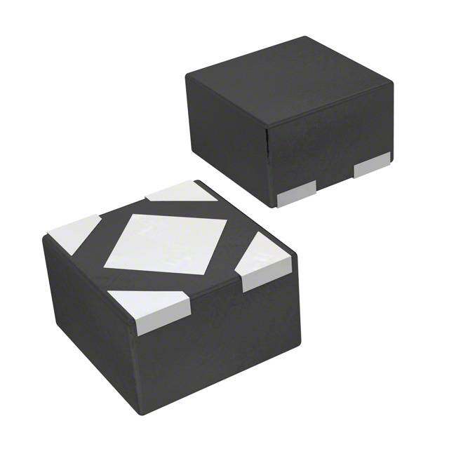
| 供应商器件封装 | 6-DFN(2x2) |
| 其它名称 | LT3008EDC-1.5#TRMPBFCT |
| 包装 | 剪切带 (CT) |
| 安装类型 | 表面贴装 |
| 封装/外壳 | 6-WFDFN 裸露焊盘 |
| 工作温度 | -40°C ~ 125°C |
| 标准包装 | 1 |
| 电压-跌落(典型值) | 0.3V @ 20mA |
| 电压-输入 | 2 V ~ 45 V |
| 电压-输出 | 1.5V |
| 电流-输出 | 20mA |
| 电流-限制(最小值) | 22mA |
| 稳压器拓扑 | 正,固定式 |
| 稳压器数 | 1 |


- 商务部:美国ITC正式对集成电路等产品启动337调查
- 曝三星4nm工艺存在良率问题 高通将骁龙8 Gen1或转产台积电
- 太阳诱电将投资9.5亿元在常州建新厂生产MLCC 预计2023年完工
- 英特尔发布欧洲新工厂建设计划 深化IDM 2.0 战略
- 台积电先进制程称霸业界 有大客户加持明年业绩稳了
- 达到5530亿美元!SIA预计今年全球半导体销售额将创下新高
- 英特尔拟将自动驾驶子公司Mobileye上市 估值或超500亿美元
- 三星加码芯片和SET,合并消费电子和移动部门,撤换高东真等 CEO
- 三星电子宣布重大人事变动 还合并消费电子和移动部门
- 海关总署:前11个月进口集成电路产品价值2.52万亿元 增长14.8%


PDF Datasheet 数据手册内容提取
LT3008 Series 3µA I , 20mA, 45V Q Low Dropout Linear Regulators FEATURES DESCRIPTION n Ultralow Quiescent Current: 3μA The LT®3008 series are micropower, low dropout voltage n Input Voltage Range: 2.0V to 45V (LDO) linear regulators. The devices supply 20mA output n Output Current: 20mA current with a dropout voltage of 300mV. No-load quiescent n Dropout Voltage: 300mV current is 3μA. Ground pin current remains at less than n Adjustable Output (V = V = 600mV) 5% of output current as load increases. In shutdown, ADJ OUT(MIN) n Fixed Output Voltages: 1.2V, 1.5V, 1.8V, 2.5V, 3.3V, 5V quiescent current is less than 1μA. n Output Tolerance: ±2% Over Load, Line and The LT3008 regulators optimize stability and transient Temperature response with low ESR ceramic capacitors, requiring a n Stable with Low ESR, Ceramic Output Capacitors minimum of only 2.2μF. The regulators do not require (2.2μF Minimum) the addition of ESR as is common with other regulators. n Shutdown Current: <1μA Internal protection circuitry includes current limiting, n Current Limit Protection thermal limiting, reverse-battery protection and reverse- n Reverse-Battery Protection current protection. n Thermal Limit Protection n TSOT-23 and 2mm × 2mm DFN Packages The LT3008 series are ideal for applications that require moderate output drive capability coupled with ultralow APPLICATIONS standby power consumption. The device is available in fi xed output voltages of 1.2V, 1.5V, 1.8V, 2.5V, 3.3V and n Automotive 5V, and an adjustable version with an output voltage range n Low Current Battery-Powered Systems of 0.6V to 44.5V. The LT3008 is available in the thermally n Keep-Alive Power Supplies enhanced 6-lead DFN and 8-lead TSOT-23 packages. n Remote Monitoring n Utility Meters L, LT, LTC, LTM, Linear Technology and the Linear logo are registered trademarks of Linear Technology Corporation. All other trademarks are the property of their respective owners. n Low Power Industrial Applications TYPICAL APPLICATION 3.3V, 20mA Supply with Shutdown Dropout Voltage/Quiescent Current 500 6 ILOAD = 20mA 3.8V4 VT5IOVN 1μF INLT3008-3.O3UT 2.2μF V32.0O3mUVTA E (mV) 434055000 DVORLOTPAOGUET 54 QUIESC AG 300 EN T T SHDNGNDSENSE 3008 TA01a ROPOUT VOL 221055000 IQ 23 CURRENT (μ D A 100 ) 1 50 0 0 –50 –25 0 25 50 75 100 125 150 TEMPERATURE (°C) 3008 TA01b 3008fc 1
LT3008 Series ABSOLUTE MAXIMUM RATINGS (Note 1) IN Pin Voltage .........................................................±50V Operating Junction Temperature Range (Notes 2, 3) OUT Pin Voltage ......................................................±50V E, I Grade ...........................................–40°C to 125°C Input-to-Output Differential Voltage ........................±50V MP Grade ...........................................–55°C to 125°C ADJ Pin Voltage ......................................................±50V Storage Temperature Range ...................–65°C to 150°C SENSE Pin Voltage ..................................................±50V Lead Temperature: Soldering, 10 sec SHDN Pin Voltage (Note 8) .....................................±50V TS8 Package Only .............................................300°C Output Short-Circuit Duration ..........................Indefi nite PIN CONFIGURATION TOP VIEW TOP VIEW **SENSE/ADJ 1 6 GND SHDN 1 8 NC OUT 2 7 5 SHDN GND 2 7 ADJ/SENSE** GND 3 6 OUT OUT 3 4 IN GND 4 5 IN TS8 PACKAGE DC PACKAGE 8-LEAD PLASTIC TSOT-23 6-LEAD (2mm (cid:115) 2mm) PLASTIC DFN TJMAX = 125°C, θJA = 65°C/W TO 85°C/W* TJMAX = 125°C, θJA = 65°C/W TO 85°C/W* EXPOSED PAD (PIN 7) IS GND, MUST BE SOLDERED TO PCB * See the Applications Information Section. ** SENSE for Fixed Voltage Output Versions. ORDER INFORMATION LEAD FREE FINISH TAPE AND REEL PART MARKING* PACKAGE DESCRIPTION TEMPERATURE RANGE LT3008EDC#PBF LT3008EDC#TRPBF LDPS 6-Lead (2mm × 2mm) Plastic DFN –40°C to 125°C LT3008IDC#PBF LT3008IDC#TRPBF LDPS 6-Lead (2mm × 2mm) Plastic DFN –40°C to 125°C LT3008EDC-1.2#PBF LT3008EDC-1.2#TRPBF LFHC 6-Lead (2mm × 2mm) Plastic DFN –40°C to 125°C LT3008IDC-1.2#PBF LT3008IDC-1.2#TRPBF LFHC 6-Lead (2mm × 2mm) Plastic DFN –40°C to 125°C LT3008EDC-1.5#PBF LT3008EDC-1.5#TRPBF LFHF 6-Lead (2mm × 2mm) Plastic DFN –40°C to 125°C LT3008IDC-1.5#PBF LT3008IDC-1.5#TRPBF LFHF 6-Lead (2mm × 2mm) Plastic DFN –40°C to 125°C LT3008EDC-1.8#PBF LT3008EDC-1.8#TRPBF LFHH 6-Lead (2mm × 2mm) Plastic DFN –40°C to 125°C LT3008IDC-1.8#PBF LT3008IDC-1.8#TRPBF LFHH 6-Lead (2mm × 2mm) Plastic DFN –40°C to 125°C LT3008EDC-2.5#PBF LT3008EDC-2.5#TRPBF LFHK 6-Lead (2mm × 2mm) Plastic DFN –40°C to 125°C LT3008IDC-2.5#PBF LT3008IDC-2.5#TRPBF LFHK 6-Lead (2mm × 2mm) Plastic DFN –40°C to 125°C LT3008EDC-3.3#PBF LT3008EDC-3.3#TRPBF LFHN 6-Lead (2mm × 2mm) Plastic DFN –40°C to 125°C LT3008IDC-3.3#PBF LT3008IDC-3.3#TRPBF LFHN 6-Lead (2mm × 2mm) Plastic DFN –40°C to 125°C LT3008EDC-5#PBF LT3008EDC-5#TRPBF LFHQ 6-Lead (2mm × 2mm) Plastic DFN –40°C to 125°C LT3008IDC-5#PBF LT3008IDC-5#TRPBF LFHQ 6-Lead (2mm × 2mm) Plastic DFN –40°C to 125°C LT3008ETS8#PBF LT3008ETS8#TRPBF LTDSX 8-Lead Plastic TSOT-23 –40°C to 125°C 3008fc 2
LT3008 Series ORDER INFORMATION LEAD FREE FINISH TAPE AND REEL PART MARKING* PACKAGE DESCRIPTION TEMPERATURE RANGE LT3008ITS8#PBF LT3008ITS8#TRPBF LTDSX 8-Lead Plastic TSOT-23 –40°C to 125°C LT3008MPTS8#PBF LT3008MPTS8#TRPBF LTDSX 8-Lead Plastic TSOT-23 –55°C to 125°C LT3008ETS8-1.2#PBF LT3008ETS8-1.2#TRPBF LTFHD 8-Lead Plastic TSOT-23 –40°C to 125°C LT3008ITS8-1.2#PBF LT3008ITS8-1.2#TRPBF LTFHD 8-Lead Plastic TSOT-23 –40°C to 125°C LT3008MPTS8-1.2#PBF LT3008MPTS8-1.2#TRPBF LTFHD 8-Lead Plastic TSOT-23 –55°C to 125°C LT3008ETS8-1.5#PBF LT3008ETS8-1.5#TRPBF LTFHG 8-Lead Plastic TSOT-23 –40°C to 125°C LT3008ITS8-1.5#PBF LT3008ITS8-1.5#TRPBF LTFHG 8-Lead Plastic TSOT-23 –40°C to 125°C LT3008MPTS8-1.5#PBF LT3008MPTS8-1.5#TRPBF LTFHG 8-Lead Plastic TSOT-23 –55°C to 125°C LT3008ETS8-1.8#PBF LT3008ETS8-1.8#TRPBF LTFHJ 8-Lead Plastic TSOT-23 –40°C to 125°C LT3008ITS8-1.8#PBF LT3008ITS8-1.8#TRPBF LTFHJ 8-Lead Plastic TSOT-23 –40°C to 125°C LT3008MPTS8-1.8#PBF LT3008MPTS8-1.8#TRPBF LTFHJ 8-Lead Plastic TSOT-23 –55°C to 125°C LT3008ETS8-2.5#PBF LT3008ETS8-2.5#TRPBF LTFHM 8-Lead Plastic TSOT-23 –40°C to 125°C LT3008ITS8-2.5#PBF LT3008ITS8-2.5#TRPBF LTFHM 8-Lead Plastic TSOT-23 –40°C to 125°C LT3008MPTS8-2.5#PBF LT3008MPTS8-2.5#TRPBF LTFHM 8-Lead Plastic TSOT-23 –55°C to 125°C LT3008ETS8-3.3#PBF LT3008ETS8-3.3#TRPBF LTFHP 8-Lead Plastic TSOT-23 –40°C to 125°C LT3008ITS8-3.3#PBF LT3008ITS8-3.3#TRPBF LTFHP 8-Lead Plastic TSOT-23 –40°C to 125°C LT3008MPTS8-3.3#PBF LT3008MPTS8-3.3#TRPBF LTFHP 8-Lead Plastic TSOT-23 –55°C to 125°C LT3008ETS8-5#PBF LT3008ETS8-5#TRPBF LTFHR 8-Lead Plastic TSOT-23 –40°C to 125°C LT3008ITS8-5#PBF LT3008ITS8-5#TRPBF LTFHR 8-Lead Plastic TSOT-23 –40°C to 125°C LT3008MPTS8-5#PBF LT3008MPTS8-5#TRPBF LTFHR 8-Lead Plastic TSOT-23 –55°C to 125°C LEAD BASED FINISH TAPE AND REEL PART MARKING* PACKAGE DESCRIPTION TEMPERATURE RANGE LT3008EDC LT3008EDC#TR LDPS 6-Lead (2mm × 2mm) Plastic DFN –40°C to 125°C LT3008IDC LT3008IDC#TR LDPS 6-Lead (2mm × 2mm) Plastic DFN –40°C to 125°C LT3008EDC-1.2 LT3008EDC-1.2#TR LFHC 6-Lead (2mm × 2mm) Plastic DFN –40°C to 125°C LT3008IDC-1.2 LT3008IDC-1.2#TR LFHC 6-Lead (2mm × 2mm) Plastic DFN –40°C to 125°C LT3008EDC-1.5 LT3008EDC-1.5#TR LFHF 6-Lead (2mm × 2mm) Plastic DFN –40°C to 125°C LT3008IDC-1.5 LT3008IDC-1.5#TR LFHF 6-Lead (2mm × 2mm) Plastic DFN –40°C to 125°C LT3008EDC-1.8 LT3008EDC-1.8#TR LFHH 6-Lead (2mm × 2mm) Plastic DFN –40°C to 125°C LT3008IDC-1.8 LT3008IDC-1.8#TR LFHH 6-Lead (2mm × 2mm) Plastic DFN –40°C to 125°C LT3008EDC-2.5 LT3008EDC-2.5#TR LFHK 6-Lead (2mm × 2mm) Plastic DFN –40°C to 125°C LT3008IDC-2.5 LT3008IDC-2.5#TR LFHK 6-Lead (2mm × 2mm) Plastic DFN –40°C to 125°C LT3008EDC-3.3 LT3008EDC-3.3#TR LFHN 6-Lead (2mm × 2mm) Plastic DFN –40°C to 125°C LT3008IDC-3.3 LT3008IDC-3.3#TR LFHN 6-Lead (2mm × 2mm) Plastic DFN –40°C to 125°C LT3008EDC-5 LT3008EDC-5#TR LFHQ 6-Lead (2mm × 2mm) Plastic DFN –40°C to 125°C LT3008IDC-5 LT3008IDC-5#TR LFHQ 6-Lead (2mm × 2mm) Plastic DFN –40°C to 125°C LT3008ETS8 LT3008ETS8#TR LTDSX 8-Lead Plastic TSOT-23 –40°C to 125°C LT3008ITS8 LT3008ITS8#TR LTDSX 8-Lead Plastic TSOT-23 –40°C to 125°C LT3008MPTS8 LT3008MPTS8#TR LTDSX 8-Lead Plastic TSOT-23 –55°C to 125°C LT3008ETS8-1.2 LT3008ETS8-1.2#TR LTFHD 8-Lead Plastic TSOT-23 –40°C to 125°C LT3008ITS8-1.2 LT3008ITS8-1.2#TR LTFHD 8-Lead Plastic TSOT-23 –40°C to 125°C LT3008MPTS8-1.2 LT3008MPTS8-1.2#TR LTFHD 8-Lead Plastic TSOT-23 –55°C to 125°C 3008fc 3
LT3008 Series ORDER INFORMATION LEAD BASED FINISH TAPE AND REEL PART MARKING* PACKAGE DESCRIPTION TEMPERATURE RANGE LT3008ETS8-1.5 LT3008ETS8-1.5#TR LTFHG 8-Lead Plastic TSOT-23 –40°C to 125°C LT3008ITS8-1.5 LT3008ITS8-1.5#TR LTFHG 8-Lead Plastic TSOT-23 –40°C to 125°C LT3008MPTS8-1.5 LT3008MPTS8-1.5#TR LTFHG 8-Lead Plastic TSOT-23 –55°C to 125°C LT3008ETS8-1.8 LT3008ETS8-1.8#TR LTFHJ 8-Lead Plastic TSOT-23 –40°C to 125°C LT3008ITS8-1.8 LT3008ITS8-1.8#TR LTFHJ 8-Lead Plastic TSOT-23 –40°C to 125°C LT3008MPTS8-1.8 LT3008MPTS8-1.8#TR LTFHJ 8-Lead Plastic TSOT-23 –55°C to 125°C LT3008ETS8-2.5 LT3008ETS8-2.5#TR LTFHM 8-Lead Plastic TSOT-23 –40°C to 125°C LT3008ITS8-2.5 LT3008ITS8-2.5#TR LTFHM 8-Lead Plastic TSOT-23 –40°C to 125°C LT3008MPTS8-2.5 LT3008MPTS8-2.5#TR LTFHM 8-Lead Plastic TSOT-23 –55°C to 125°C LT3008ETS8-3.3 LT3008ETS8-3.3#TR LTFHP 8-Lead Plastic TSOT-23 –40°C to 125°C LT3008ITS8-3.3 LT3008ITS8-3.3#TR LTFHP 8-Lead Plastic TSOT-23 –40°C to 125°C LT3008MPTS8-3.3 LT3008MPTS8-3.3#TR LTFHP 8-Lead Plastic TSOT-23 –55°C to 125°C LT3008ETS8-5 LT3008ETS8-5#TR LTFHR 8-Lead Plastic TSOT-23 –40°C to 125°C LT3008ITS8-5 LT3008ITS8-5#TR LTFHR 8-Lead Plastic TSOT-23 –40°C to 125°C LT3008MPTS8-5 LT3008MPTS8-5#TR LTFHR 8-Lead Plastic TSOT-23 –55°C to 125°C Consult LTC Marketing for parts specifi ed with wider operating temperature ranges. *The temperature grade is identifi ed by a label on the shipping container. For more information on lead free part marking, go to: http://www.linear.com/leadfree/ For more information on tape and reel specifi cations, go to: http://www.linear.com/tapeandreel/ ELECTRICAL CHARACTERISTICS The l denotes the specifi cations which apply over the full operating temperature range, otherwise specifi cations are at T = 25°C. (Note 2) J PARAMETER CONDITIONS MIN TYP MAX UNITS Operating Voltage l 2 45 V Regulated Output Voltage LT3008-1.2: V = 2V, I = 100μA 1.188 1.2 1.212 V IN LOAD 2V < V < 45V, 1μA < I < 20mA l 1.176 1.2 1.224 V IN LOAD LT3008-1.5: V = 2.05V, I = 100μA 1.485 1.5 1.515 V IN LOAD 2.05V < V < 45V, 1μA < I < 20mA l 1.47 1.5 1.53 V IN LOAD LT3008-1.8: V = 2.35V, I = 100μA 1.782 1.8 1.818 V IN LOAD 2.35V < V < 45V, 1μA < I < 20mA l 1.764 1.8 1.836 V IN LOAD LT3008-2.5: V = 3.05V, I = 100μA 2.475 2.5 2.525 V IN LOAD 3.05V < V < 45V, 1μA < I < 20mA l 2.45 2.5 2.55 V IN LOAD LT3008-3.3: V = 3.85V, I = 100μA 3.267 3.3 3.333 V IN LOAD 3.85V < V < 45V, 1μA < I < 20mA l 3.234 3.3 3.366 V IN LOAD LT3008-5: V = 5.55V, I = 100μA 4.95 5 5.05 V IN LOAD 5.55V < V < 45V, 1μA < I < 20mA l 4.9 5 5.1 V IN LOAD ADJ Pin Voltage (Notes 3, 4) V = 2V, I = 100μA 594 600 606 mV IN LOAD 2V < V < 45V, 1μA < I < 20mA l 588 600 612 mV IN LOAD Line Regulation (Note 3) LT3008-1.2: ΔV = 2V to 45V, I = 1mA l 1.2 6 mV IN LOAD LT3008-1.5: ΔV = 2.05V to 45V, I = 1mA l 1.5 7.5 mV IN LOAD LT3008-1.8: ΔV = 2.35V to 45V, I = 1mA l 1.8 9 mV IN LOAD LT3008-2.5: ΔV = 3.05V to 45V, I = 1mA l 2.5 12.5 mV IN LOAD LT3008-3.3: ΔV = 3.85V to 45V, I = 1mA l 3.3 16.5 mV IN LOAD LT3008-5: ΔV = 5.55V to 45V, I = 1mA l 5 25 mV IN LOAD LT3008: ΔV = 2V to 45V, I = 1mA l 0.6 3 mV IN LOAD 3008fc 4
LT3008 Series ELECTRICAL CHARACTERISTICS The l denotes the specifi cations which apply over the full operating temperature range, otherwise specifi cations are at T = 25°C. (Note 2) J PARAMETER CONDITIONS MIN TYP MAX UNITS Load Regulation (Note 3) LT3008-1.2: V = 2V, I = 1μA to 10mA l 0.8 4 mV IN LOAD V = 2V, I = 1μA to 20mA l 1 10 mV IN LOAD LT3008-1.5: V = 2.05V, I = 1μA to 10mA l 1 5 mV IN LOAD V = 2.05V, I = 1μA to 20mA l 1.3 13 mV IN LOAD LT3008-1.8: V = 2.35V, I = 1μA to 10mA l 1.2 6 mV IN LOAD V = 2.35V, I = 1μA to 20mA l 1.5 15 mV IN LOAD LT3008-2.5: V = 3.05V, I = 1μA to 10mA l 1.7 8.3 mV IN LOAD V = 3.05V, I = 1μA to 20mA l 2.1 21 mV IN LOAD LT3008-3.3: V = 3.85V, I = 1μA to 10mA l 2.2 11 mV IN LOAD V = 3.85V, I = 1μA to 20mA l 2.8 28 mV IN LOAD LT3008-5: V = 5.55V, I = 1μA to 10mA l 3.4 17 mV IN LOAD V = 5.55V, I = 1μA to 20mA l 4.2 42 mV IN LOAD LT3008: V = 2V, I = 1μA to 10mA l 0.4 2 mV IN LOAD V = 2V, I = 1μA to 20mA l 0.5 5 mV IN LOAD Dropout Voltage I = 100μA 115 180 mV LOAD V = V (Notes 5, 6) I = 100μA l 250 mV IN OUT(NOMINAL) LOAD I = 1mA 170 250 mV LOAD I = 1mA l 350 mV LOAD I = 10mA 270 340 mV LOAD I = 10mA l 470 mV LOAD I = 20mA 300 365 mV LOAD I = 20mA l 500 mV LOAD Quiescent Current (Notes 6, 7) I = 0μA 3 μA LOAD I = 0μA l 6 μA LOAD GND Pin Current I = 0μA l 3 6 μA LOAD V = V + 0.5V (Notes 6, 7) I = 100μA l 6 12 μA IN OUT(NOMINAL) LOAD I = 1mA l 21 50 μA LOAD I = 10mA l 160 500 μA LOAD I = 20mA l 350 1200 μA LOAD Output Voltage Noise (Note 9) C = 2.2μF, I = 20mA, BW = 10Hz to 100kHz 92 μV OUT LOAD RMS ADJ Pin Bias Current –10 0.4 10 nA Shutdown Threshold V = Off to On l 0.67 1.5 V OUT V = On to Off l 0.25 0.61 V OUT SHDN Pin Current VSHDN = 0V, VIN = 45V l ±1 μA V = 45V, V = 45V l 0.65 2 μA SHDN IN Quiescent Current in Shutdown V = 6V, V = 0V l <1 μA IN SHDN Ripple Rejection (Note 3) V – V = 2V, V = 0.5V , IN OUT RIPPLE P-P f = 120Hz, I = 20mA RIPPLE LOAD LT3008 58 70 dB LT3008-1.2 54 66 dB LT3008-1.5 53 65 dB LT3008-1.8 52 64 dB LT3008-2.5 49 61 dB LT3008-3.3 47 59 dB LT3008-5 42 54 dB 3008fc 5
LT3008 Series ELECTRICAL CHARACTERISTICS The l denotes the specifi cations which apply over the full operating temperature range, otherwise specifi cations are at T = 25°C. (Note 2) J PARAMETER CONDITIONS MIN TYP MAX UNITS Current Limit V = 45V, V = 0 75 mA IN OUT V = V + 1V, ΔV = –5% l 22 mA IN OUT(NOMINAL) OUT Input Reverse-Leakage Current V = –45V, V = 0 l 1 30 μA IN OUT Reverse-Output Current V = 1.2V, V = 0 0.6 10 μA OUT IN Note 1: Stresses beyond those listed under Absolute Maximum Ratings Note 5: Dropout voltage is the minimum input to output voltage differential may cause permanent damage to the device. Exposure to any Absolute needed to maintain regulation at a specifi ed output current. In dropout, the Maximum Rating condition for extended periods may affect device output voltage equals (V – V ). For the LT3008-1.2 and LT3008- IN DROPOUT reliability and lifetime. 1.5, dropout voltage will be limited by the minimum input voltage. Note 2: The LT3008 regulators are tested and specifi ed under pulse Note 6: To satisfy minimum input voltage requirements, the LT3008 load conditions such that TJ ≅ TA. The LT3008E is guaranteed to meet adjustable version is tested and specifi ed for these conditions with an performance specifi cations from 0°C to 125°C operating junction external resistor divider (61.9k bottom, 280k top) which sets V to 3.3V. OUT temperature. Specifi cations over the –40°C to 125°C operating junction The external resistor divider adds 9.69μA of DC load on the output. This temperature range are assured by design, characterization and correlation external current is not factored into GND pin current. with statistical process controls. The LT3008I is guaranteed over the full Note 7: GND pin current is tested with V = V + 0.55V and IN OUT(NOMINAL) –40°C to 125°C operating junction temperature range. The LT3008MP is a current source load. GND pin current will increase in dropout. For the 100% tested and guaranteed over the –55°C to 125°C operating junction fi xed output voltage versions, an internal resistor divider will add about temperature range. 1μA to the GND pin current. See the GND Pin Current curves in the Typical Note 3: The LT3008 adjustable version is tested and specifi ed for these Performance Characteristics section. conditions with the ADJ pin connected to the OUT pin. Note 8: The SHDN pin can be driven below GND only when tied to the IN Note 4: Operating conditions are limited by maximum junction pin directly or through a pull-up resistor. If the SHDN pin is driven below temperature. The regulated output voltage specifi cation will not apply GND by more than –0.3V while IN is powered, the output will turn on. for all possible combinations of input voltage and output current. When Note 9: Output noise is listed for the adjustable version with the ADJ pin operating at the maximum input voltage, the output current range must be connected to the OUT pin. See the RMS Output Noise vs Load Current limited. When operating at the maximum output current, the input voltage curve in the Typical Performance Characteristics Section. must be limited. 3008fc 6
LT3008 Series TYPICAL PERFORMANCE CHARACTERISTICS T = 25°C, unless otherwise noted. A Dropout Voltage Dropout Voltage Minimum Input Voltage 450 450 2 ILOAD = 20mA 400 400 1.8 mV)350 TJ = 125°C mV)350 20mA GE (V)11..46 OUT VOLTAGE (223050000 TJ = 25°C OUT VOLTAGE (223050000 1mA 10mA M INPUT VOLTA 01..182 DROP110500 DROP110500 100μA MINIMU 00..64 50 50 0.2 0 0 0 0 2 4 6 8 10 12 14 16 18 20 –50 –25 0 25 50 75 100 125 150 –50 –25 0 25 50 75 100 125 150 OUTPUT CURRENT (mA) TEMPERATURE (°C) TEMPERATURE (°C) 3008 G01 3008 G02 3008 G03 Output Voltage Output Voltage ADJ Pin Voltage LT3008-1.2 LT3008-1.5 0.612 1.224 1.530 0.610 IL = 100μA 1.220 ILOAD = 100μA 1.525 ILOAD = 100μA 0.608 1.216 1.520 0.606 1.212 1.515 V) V) V) E (0.604 E (1.208 E (1.510 AG0.602 AG1.204 AG1.505 T T T OL0.600 OL1.200 OL1.500 V V V N 0.598 T 1.196 T 1.495 J PI0.596 TPU1.192 TPU1.490 D U U A0.594 O1.188 O1.485 0.592 1.184 1.480 0.590 1.180 1.475 0.588 1.176 1.470 –50 –25 0 25 50 75 100 125 150 –50 –25 0 25 50 75 100 125 150 –50 –25 0 25 50 75 100 125 150 TEMPERATURE (°C) TEMPERATURE (°C) TEMPERATURE (°C) 3008 G05 3008 G06 3008 G04 Output Voltage Output Voltage Output Voltage LT3008-1.8 LT3008-2.5 LT3008-3.3 1.836 2.550 3.366 1.830 ILOAD = 100μA 2.540 ILOAD = 100μA 3.355 ILOAD = 100μA 1.824 3.344 2.530 1.816 3.333 E (V)1.812 E (V)2.520 E (V)3.322 AG1.806 AG2.510 AG3.311 T T T OL1.800 OL2.500 OL3.300 V V V UT 1.794 UT 2.490 UT 3.289 TP1.788 TP TP3.278 U U2.480 U O1.782 O O3.267 2.470 1.776 3.256 1.770 2.460 3.245 1.764 2.450 3.234 –50 –25 0 25 50 75 100 125 150 –50 –25 0 25 50 75 100 125 150 –50 –25 0 25 50 75 100 125 150 TEMPERATURE (°C) TEMPERATURE (°C) TEMPERATURE (°C) 3008 G07 3008 G08 3008 G09 3008fc 7
LT3008 Series TYPICAL PERFORMANCE CHARACTERISTICS T = 25°C, unless otherwise noted. A Output Voltage LT3008-5 ADJ Pin Bias Current Adjustable Quiescent Current 5.100 10 6 ILOAD = 100μA 5.075 8 5 OUTPUT VOLTAGE (V)54455.....099000752505050 J PIN BIAS CURRENT (nA) ––440622 UIESCENT CURRENT (μA) 324 AD –6 Q 1 4.925 –8 4.900 –10 0 –50 –25 0 25 50 75 100 125 150 –50 –25 0 25 50 75 100 125 150 –50 –25 0 25 50 75 100 125 150 TEMPERATURE (°C) TEMPERATURE (°C) TEMPERATURE (°C) 3008 G10 3008 G05 3008 G06 GND Pin Current GND Pin Current Quiescent Current LT3008-1.2 LT3008-1.5 30 500 500 LT3008-1.2 27 LT3008-1.5 450 450 24 LT3008-1.8 400 400 NT (μA) 21 LLLTTT333000000888---235..53 T (μA)350 RL = 60Ω, IL = 20mA T (μA)350 RL = 75Ω, IL = 20mA RE 18 EN300 EN300 R R R CU 15 UR250 UR250 UIESCENT 129 GND PIN C210500 RL = 120Ω, IL = 10mA GND PIN C210500 RL = 150Ω, IL = 10mA Q 6 100 RL = 12k, IL = 100μA 100 RL = 15k, IL = 100μA 3 50 RL = 1.2k, IL = 1mA 50 RL = 1.5k, IL = 1mA 0 0 0 0 1 2 3 4 5 6 7 8 9 10 0 1 2 3 4 5 6 7 8 9 10 0 1 2 3 4 5 6 7 8 9 10 INPUT VOLTAGE (V) INPUT VOLTAGE (V) INPUT VOLTAGE (V) 3008 G14 3008 G15 3008 G13 GND Pin Current GND Pin Current GND Pin Current LT3008-1.8 LT3008-2.5 LT3008-3.3 500 500 500 450 450 450 400 400 400 T (μA)350 RL = 90Ω, IL = 20mA T (μA)350 RL = 125Ω, IL = 20mA T (μA)350 RL = 165Ω, IL = 20mA N300 N300 N300 E E E R R R UR250 UR250 UR250 C C C N 200 N 200 N 200 ND PI150 RL = 180Ω, IL = 10mA ND PI150 RL = 250Ω, IL = 10mA ND PI150 RL = 330Ω, IL = 10mA G G G 100 RL = 18k, IL = 100μA 100 RL = 25k, IL = 100μA 100 RL = 33k, IL = 100μA 50 RL = 1.8k, IL = 1mA 50 RL = 2.5k, IL = 1mA 50 RL = 3.3k, IL = 1mA 0 0 0 0 1 2 3 4 5 6 7 8 9 10 0 1 2 3 4 5 6 7 8 9 10 0 1 2 3 4 5 6 7 8 9 10 INPUT VOLTAGE (V) INPUT VOLTAGE (V) INPUT VOLTAGE (V) 3008 G16 3008 G17 3008 G18 3008fc 8
LT3008 Series TYPICAL PERFORMANCE CHARACTERISTICS T = 25°C, unless otherwise noted. A GND Pin Current LT3008-5 GND Pin Current vs I SHDN Pin Thresholds LOAD 500 1000 1.5 VIN = 3.8V 1.4 450 VOUT = 3.3V 1.3 400 1.2 GND PIN CURRENT (μA)223135055000000 RRLL == 520500ΩΩ,, IILL == 1200mmAA GND CURRENT (μA) 11000 HDN PIN THRESHOLD (V) 0000100.......98761451 OONFF T TOO O OFNF 100 RL = 50k, IL = 100μA S 0.3 0.2 50 RL = 5k, IL = 1mA 0.1 0 1 0 0 1 2 3 4 5 6 7 8 9 10 0.001 0.01 0.1 1 10 100 –50 –25 0 25 50 75 100 125 150 INPUT VOLTAGE (V) LOAD (mA) TEMPERATURE (°C) 3008 G19 3008 G20 3008 G21 SHDN Pin Input Current SHDN Pin Input Current Current Limit 2 2 100 1.8 1.8 90 μA) 1.6 μA) 1.6 80 VIN = 45V ENT ( 1.4 ENT ( 1.4 mA) 70 RR 1.2 RR 1.2 T ( 60 UT CU 1 UT CU 1 T LIMI 50 N INP 0.8 N INP 0.8 VSHDN = 45V RREN 40 VIN = 2V N PI 0.6 N PI 0.6 CU 30 HD 0.4 HD 0.4 20 S S 0.2 0.2 10 0 0 0 0 5 10 15 20 25 30 35 40 45 –50 –25 0 25 50 75 100 125 150 –50 –25 0 25 50 75 100 125 150 SHDN PIN VOLTAGE (V) TEMPERATURE (°C) TEMPERATURE (°C) 3008 G22 3008 G23 3008 G24 Reverse-Output Current Input Ripple Rejection Input Ripple Rejection 50 90 80 OUT = ADJ = 1.2V VIN = 2.1V + 50mVRMS 45 IN = SHDN = GND 80 VOUT = 600mV 70 URRENT (μA) 343500 CTION (dB) 7600 ILOAD = 20mA ECTION (dB) 6500 REVERSE OUTPUT C 221150055 ADJ INPUT RIPPLE REJE 1532400000 2.2μF10μF INPUT RIPPLE REJ 34210000 RVIINP P=L VEO AUTT f( N=O 1M20INHAzL) + 2V + 0.5VP-P OUT ILOAD = 20mA 0 0 0 –50 –25 0 25 50 75 100 125 150 10 100 1000 10000 100000 1000000 –50 –25 0 25 50 75 100 125 150 TEMPERATURE (°C) FREQUENCY (Hz) TEMPERATURE (°C) 3008 G25 3008 G26 3008 G27 3008fc 9
LT3008 Series TYPICAL PERFORMANCE CHARACTERISTICS T = 25°C, unless otherwise noted. A RMS Output Noise Load Regulation Output Noise Spectral Density vs Load Current 5 100 500 mV) 34..554 V(cid:36)VOIINLU ==T =21μ V6A0 0tom 2V0mA SITY (μV Hz) CILOOUATD == 22.02mμFA 53211V....3585VVVV )MS344550000 COUT = 10μF 35.3VV AD REGULATION ( 21..2553 SE SPECTRAL DEN 101 10V.6V UTPUT NOISE (μVR321205500000 12..85V1V.5V LO 1 T NOI O 100 1.2V U 0.5 TP 50 0.6V U 0 O 0.1 0 –50 –25 0 25 50 75 100 125 150 10 100 1k 10k 100k 0.001 0.01 0.1 1 10 100 TEMPERATURE (°C) FREQUENCY (Hz) ILOAD (mA) 3008 G28 3008 G29 3008 G30 Transient Response Transient Response Transient Response (Load Dump) IOUT = 1mA TO 20mA IOUT = 1mA TO 20mA VIN = 5.5V VIN = 5.5V VOUT = 5V VOUT = 5V VOUT COUT = 2.2μF COUT = 10μF 50mV/DIV 50mVV/ODUIVT 50mVV/ODUIVT 45V VOUT = 5V IOUT IOUT 10V/DVIIVN ICOOUUTT = = 2 40.m7μAF 12V 20mA/DIV 20mA/DIV 500μs/DIV 3008 G31 500μs/DIV 3008 G32 1ms/DIV 3008 G33 3008fc 10
LT3008 Series PIN FUNCTIONS (TSOT-23/DFN) SHDN (Pin 1/Pin 5): Shutdown. Pulling the SHDN pin Temperature in the Typical Performance Characteristics low puts the LT3008 into a low power state and turns the section). The ADJ pin voltage is 600mV referenced to GND output off. If unused, tie the SHDN pin to V . The LT3008 and the output voltage range is 600mV to 44.5V. IN does not function if the SHDN pin is not connected. The NC (Pin 8, TSOT-23 Package Only): No Connect. Pin 8 SHDN pin cannot be driven below GND unless tied to the is an NC pin in the TSOT-23 package. This pin is not tied IN pin. If the SHDN pin is driven below GND while IN is to any internal circuitry. It may be fl oated, tied to V or IN powered, the output will turn on. SHDN pin logic cannot tied to GND. be referenced to a negative rail. GND (Exposed Pad Pin 7, DFN Package Only): Ground. The GND (Pins 2, 3, 4/Pin 6): Ground. Connect the bottom exposed pad (backside) of the DFN package is an electrical of the resistor divider that sets output voltage directly to connection to GND. To ensure optimum performance, GND for the best regulation. solder Pin 7 to the PCB and tie directly to Pin 6. IN (Pin 5/Pin 4): Input. The IN pin supplies power to the SENSE (Pin 7/Pin 1): Sense. For fi xed voltage versions of device. The LT3008 requires a bypass capacitor at IN if the LT3008 (LT3008-1.2, LT3008-1.5, LT3008-1.8, LT3008- the device is more than six inches away from the main 2.5, LT3008-3.3, LT3008-5), the SENSE pin is the input to input fi lter capacitor. In general, the output impedance of the error amplifi er. Optimum regulation is obtained at the a battery rises with frequency, so it is advisable to include point where the SENSE pin is connected to the OUT pin of a bypass capacitor in battery-powered circuits. A bypass the regulator. In critical applications, small voltage drops capacitor in the range of 0.1μF to 10μF will suffi ce. The are caused by the resistance (RP) of PC traces between LT3008 withstands reverse voltages on the IN pin with the regulator and the load. These may be eliminated by respect to ground and the OUT pin. In the case of a reversed connecting the SENSE pin to the output at the load as input, which occurs with a battery plugged in backwards, shown in Figure 1 (Kelvin Sense Connection). Note that the LT3008 acts as if a blocking diode is in series with its the voltage drop across the external PC traces add to the input. No reverse current fl ows into the LT3008 and no dropout voltage of the regulator. The SENSE pin bias current reverse voltage appears at the load. The device protects is 1μA at the nominal rated output voltage. The SENSE pin both itself and the load. can be pulled below ground (as in a dual supply system where the regulator load is returned to a negative supply) OUT (Pin 6/Pins 2, 3): Output. This pin supplies power and still allow the device to start and operate. to the load. Use a minimum output capacitor of 2.2μF to prevent oscillations. Large load transient applications RP require larger output capacitors to limit peak voltage IN OUT transients. See the Applications Information section for LT3008 more information on output capacitance and reverse-output + SHDN SENSE + characteristics. VIN LOAD GND ADJ (Pin 7/Pin 1): Adjust. This pin is the error amplifi er’s RP 3008 F01 inverting terminal. Its 400pA typical input bias current fl ows out of the pin (see curve of ADJ Pin Bias Current vs Figure 1. Kelvin Sense Connection 3008fc 11
LT3008 Series APPLICATIONS INFORMATION The LT3008 is a low dropout linear regulator with ultra- to insure stability under minimum load conditions. In low quiescent current and shutdown. Quiescent current shutdown, the output turns off and the divider current is is extremely low at 3μA and drops well below 1μA in zero. Curves of ADJ Pin Voltage vs Temperature and ADJ shutdown. The device supplies up to 20mA of output current. Pin Bias Current vs Temperature appear in the Typical Dropout voltage at 20mA is typically 300mV. The LT3008 Performance Characteristics. incorporates several protection features, making it ideal for Specifi cations for output voltages greater than 0.6V are use in battery-powered systems. The device protects itself proportional to the ratio of the desired output voltage to against both reverse-input and reverse-output voltages. 0.6V: V /0.6V. For example, load regulation for an output OUT In battery backup applications, where a backup battery current change of 100μA to 20mA is –0.5mV typical at holds up the output when the input is pulled to ground, V = 0.6V. At V = 5V, load regulation is: OUT OUT the LT3008 acts as if a blocking diode is in series with its output and prevents reverse current fl ow. In applications 5V •(−0.5mV)=−4.17mV where the regulator load returns to a negative supply, the 0.6V output can be pulled below ground by as much as 50V Table 1 shows resistor divider values for some com- without affecting start-up or normal operation. mon output voltages with a resistor divider current of Adjustable Operation about 1μA. The LT3008 has an output voltage range of 0.6V to 44.5V. Table 1. Output Voltage Resistor Divider Values Figure 2 shows that output voltage is set by the ratio of two V R1 R2 OUT external resistors. The IC regulates the output to maintain 1V 604k 402k the ADJ pin voltage at 600mV referenced to ground. The 1.2V 590k 590k current in R1 equals 600mV/R1 and the current in R2 is 1.5V 590k 887k the current in R1 minus the ADJ pin bias current. The ADJ 1.8V 590k 1.18M pin bias current, typically 400pA at 25°C, fl ows out of the 2.5V 590k 1.87M pin. Calculate the output voltage using the formula in Figure 3V 590k 2.37M 2. An R1 value of 619k sets the divider current to 0.97μA. 3.3V 619k 2.8M Do not make R1’s value any greater than 619k to minimize output voltage errors due to the ADJ pin bias current and 5V 590k 4.32M VOUT = 600mV • (1 + R2/R1) – (IADJ • R2) IN OUT VOUT VADJ = 600mV VIN LT3008 R2 IADJ = 0.4nA at 25°C OUTPUT RANGE = 0.6V to 44.5V SHDN ADJ GND R1 3008 F02 Figure 2. Adjustable Operation 3008fc 12
LT3008 Series APPLICATIONS INFORMATION Because the ADJ pin is relatively high impedance (de- Give extra consideration to the use of ceramic capacitors. pending on the resistor divider used), stray capacitances Manufacturers make ceramic capacitors with a variety of at this pin should be minimized. Special attention should dielectrics, each with different behavior across temperature be given to any stray capacitances that can couple ex- and applied voltage. The most common dielectrics are ternal signals onto the ADJ pin, producing undesirable specifi ed with EIA temperature characteristic codes of output transients or ripple. Z5U, Y5V, X5R and X7R. The Z5U and Y5V dielectrics provide high C-V products in a small package at low cost, Extra care should be taken in assembly when using high but exhibit strong voltage and temperature coeffi cients as valued resistors. Small amounts of board contamination shown in Figures 3 and 4. When used with a 5V regulator, can lead to signifi cant shifts in output voltage. Appropriate a 16V 10μF Y5V capacitor can exhibit an effective value post-assembly board cleaning measures should be as low as 1μF to 2μF for the DC bias voltage applied and implemented to prevent board contamination. If the over the operating temperature range. The X5R and board is to be subjected to humidity cycling or if board X7R dielectrics yield more stable characteristics and are cleaning measures cannot be guaranteed, consideration more suitable for use as the output capacitor. The X7R should be given to using resistors an order of magnitude type has better stability across temperature, while the smaller than in Table 1 to prevent contamination from X5R is less expensive and is available in higher values. causing unwanted shifts in the output voltage. A fi xed One must still exercise care when using X5R and X7R voltage option in the LT3008 series will not need these capacitors; the X5R and X7R codes only specify operating special considerations. temperature range and maximum capacitance change Output Capacitance and Transient Response over temperature. Capacitance change due to DC bias with X5R and X7R capacitors is better than Y5V and Z5U The LT3008 is stable with a wide range of output capacitors. capacitors, but can still be signifi cant enough to drop The ESR of the output capacitor affects stability, most capacitor values below appropriate levels. Capacitor DC notably with small capacitors. Use a minimum output bias characteristics tend to improve as component case capacitor of 2.2μF with an ESR of 3Ω or less to prevent size increases, but expected capacitance at operating oscillations. The LT3008 is a micropower device and output voltage should be verifi ed. load transient response is a function of output capacitance. Larger values of output capacitance decrease the peak Voltage and temperature coeffi cients are not the only deviations and provide improved transient response for sources of problems. Some ceramic capacitors have a larger load current changes. 20 40 BOTH CAPACITORS ARE 16V, 1210 CASE SIZE, 10μF 20 0 %) X5R %) 0 X5R E (–20 E ( U U L L –20 A A V V N –40 N E I E I –40 G G Y5V N N A–60 A H H –60 C Y5V C –80 –80 BOTH CAPACITORS ARE 16V, 1210 CASE SIZE, 10μF –100 –100 0 2 4 6 8 10 12 14 16 –50 –25 0 25 50 75 100 125 DC BIAS VOLTAGE (V) TEMPERATURE (°C) 3008 F03 3008 F04 Figure 3. Ceramic Capacitor DC Bias Characteristics Figure 4. Ceramic Capacitor Temperature Characteristics 3008fc 13
LT3008 Series APPLICATIONS INFORMATION piezoelectric response. A piezoelectric device generates GND pin current is found by examining the GND Pin voltage across its terminals due to mechanical stress, Current curves in the Typical Performance Characteristics similar to the way a piezoelectric accelerometer or section. Power dissipation is equal to the sum of the two microphone works. For a ceramic capacitor, the stress components listed prior. can be induced by vibrations in the system or thermal The LT3008 regulator has internal thermal limiting designed transients. The resulting voltages produced can cause to protect the device during overload conditions. For appreciable amounts of noise, especially when a ceramic continuous normal conditions, do not exceed the maximum capacitor is used for noise bypassing. A ceramic capacitor junction temperature rating of 125°C. Carefully consider produced Figure 5’s trace in response to light tapping from a all sources of thermal resistance from junction to ambient pencil. Similar vibration induced behavior can masquerade including other heat sources mounted in proximity to as increased output voltage noise. the LT3008. For surface mount devices, heat sinking is accomplished by using the heat spreading capabilities of the PC board and its copper traces. Copper board stiffeners VOUT = 0.6V COUT = 22μF and plated through-holes can also be used to spread the ILOAD = 10μA heat generated by power devices. VOUT The following tables list thermal resistance for several 500μV/DIV different board sizes and copper areas. All measurements were taken in still air on 3/32" FR-4 two-layer boards with one ounce copper. 100ms/DIV 3008 F05 PCB layers, copper weight, board layout and thermal vias affect the resultant thermal resistance. Although Tables Figure 5. Noise Resulting from Tapping 2 and 3 provide thermal resistance numbers for 2-layer on a Ceramic Capacitor boards with 1 ounce copper, modern multilayer PCBs provide better performance than found in these tables. Thermal Considerations The LT3008’s maximum rated junction temperature of Table 2: Measured Thermal Resistance for DC Package 125°C limits its power-handling capability. Two components COPPER AREA BOARD THERMAL RESISTANCE comprise the power dissipated by the device: TOPSIDE* BACKSIDE AREA (JUNCTION-TO-AMBIENT) 2500mm2 2500mm2 2500mm2 65°C/W 1. Output current multiplied by the input/output voltage differential: I • (V – V ) 1000mm2 2500mm2 2500mm2 70°C/W OUT IN OUT 225mm2 2500mm2 2500mm2 75°C/W 2. GND pin current multiplied by the input voltage: 100mm2 2500mm2 2500mm2 80°C/W I • V GND IN 50mm2 2500mm2 2500mm2 85°C/W *Device is mounted on the topside. 3008fc 14
LT3008 Series APPLICATIONS INFORMATION So, Table 3: Measured Thermal Resistance for TSOT-23 Package COPPER AREA P = 20mA(12.6V – 3.3V) + 0.3mA(12.6V) = 189.8mW BOARD THERMAL RESISTANCE TOPSIDE* BACKSIDE AREA (JUNCTION-TO-AMBIENT) The thermal resistance ranges from 65°C/W to 85°C/W 2500mm2 2500mm2 2500mm2 65°C/W depending on the copper area. So, the junction temperature 1000mm2 2500mm2 2500mm2 67°C/W rise above ambient approximately equals: 225mm2 2500mm2 2500mm2 70°C/W 0.1898W(75°C/W) = 14.2°C 100mm2 2500mm2 2500mm2 75°C/W 50mm2 2500mm2 2500mm2 85°C/W The maximum junction temperature equals the maximum *Device is mounted on the topside. junction temperature rise above ambient plus the maximum ambient temperature or: For example, a 4-layer, 1 ounce copper PCB board with T = 85°C + 14.2°C = 99.2°C 3 thermal vias from the DFN exposed backside or the J(MAX) 3 fused TSOT-23 GND pins to inner layer GND planes Protection Features achieves 45°C/W thermal resistance. Demo circuit DC 1388A’s board layout achieves this 45°C/W performance. The LT3008 incorporates several protection features that This is approximately a 30% improvement over the lowest make it ideal for use in battery-powered circuits. In ad- numbers shown in Tables 2 and 3. dition to the normal protection features associated with monolithic regulators, such as current limiting and thermal Calculating Junction Temperature limiting, the device also protects against reverse-input voltages, reverse-output voltages and reverse output-to- Example: Given an output voltage of 3.3V, an input voltage input voltages. range of 12V ±5%, an output current range of 0mA to 20mA and a maximum ambient temperature of 85°C, what will Current limit protection and thermal overload protec- the maximum junction temperature be for an application tion protect the device against current overload condi- using the DC package? tions at the output of the device. For normal operation, do not exceed a junction temperature of 125°C. The The power dissipated by the device is equal to: typical thermal shutdown circuitry temperature threshold I (V – V ) + I (V ) OUT(MAX) IN(MAX) OUT GND IN(MAX) is 160°C. where, The IN pin withstands reverse voltages of 50V. The device I = 20mA limits current fl ow to less than 30μA (typically less than OUT(MAX) 1μA) and no negative voltage appears at OUT. The device V = 12.6V IN(MAX) protects both itself and the load against batteries that are I at (I = 20mA, V = 12.6V) = 0.3mA plugged in backwards. GND OUT IN 3008fc 15
LT3008 Series APPLICATIONS INFORMATION The SHDN pin cannot be driven below GND unless tied to to ground, pulled to some intermediate voltage or is left the IN pin. If the SHDN pin is driven below GND while IN open circuit. Current fl ow back into the output follows the is powered, the output will turn on. SHDN pin logic cannot curve shown in Figure 6. be referenced to a negative rail. If the LT3008 IN pin is forced below the OUT pin or the The LT3008 incurs no damage if OUT is pulled below OUT pin is pulled above the IN pin, input current typically ground. If IN is left open circuit or grounded, OUT can be drops to less than 1μA. This occurs if the LT3008 input is pulled below ground by 50V. No current fl ows from the connected to a discharged (low voltage) battery and either pass transistor connected to OUT. However, current fl ows a backup battery or a second regulator circuit holds up in (but is limited by) the resistor divider that sets output the output. The state of the SHDN pin has no effect in the voltage. Current fl ows from the bottom resistor in the reverse current if OUT is pulled above IN. divider and from the ADJ pin’s internal clamp through the top resistor in the divider to the external circuitry pulling 100 OUT below ground. If IN is powered by a voltage source, 90 OUT sources current equal to its current limit capability and 80 A) the LT3008 protects itself by thermal limiting if necessary. T (μ 70 ADJ CURRENT In this case, grounding the SHDN pin turns off the LT3008 EN 60 R R and stops OUT from sourcing current. U 50 C SE 40 R The LT3008 incurs no damage if the ADJ pin is pulled E V 30 E above or below ground by 50V. If IN is left open circuit or R 20 OUT CURRENT grounded, ADJ acts like a 100k resistor in series with a 10 diode when pulled above or below ground. 0 0 1 2 3 4 5 6 7 8 9 10 In circuits where a backup battery is required, several OUTPUT AND ADJ VOLTAGE (V) 3008 F06 different input/output conditions can occur. The output voltage may be held up while the input is either pulled Figure 6. Reverse-Output Current 3008fc 16
LT3008 Series TYPICAL APPLICATIONS Keep-Alive Power Supply NO PROTECTION DIODES NEEDED! VIN IN OUT 3.3V 12V 1μF LT3008-3.3 2.2μF LOAD: SHDN SENSE SYSTEM MONITOR, GND VOLATILE MEMORY, ETC. 3009 TA02 Last-Gasp Circuit VLINE LINE POWER SENSE 12V TO 15V DCHARGE LINE INTERRUPT RLIMIT DETECT 5V TO IN OUT PWR FAULT MONITORING CENTER SUPERCAP 1μF LT3008-5 2.2μF GND 3008 TA03 SHDN SENSE GND PACKAGE DESCRIPTION DC6 Package 6-Lead Plastic DFN (2mm × 2mm) (Reference LTC DWG # 05-08-1703 Rev B) R = 0.125 0.40 ±0.10 TYP 0.56 ±0.05 4 6 0.70 ±0.05 (2 SIDES) 2.55 ±0.05 1.15 ±0.050.61 ±0.05 2.00 ±0.10 PIN 1 NOTCH (2 SIDES) POAUCTKLIANGEE (SETPEOI NPN OM1T BAEAR 6RK) (4 SIDES) R0C.H 2=A5 0M ×.2F 40E5 RO° R R = 0.05 (DC6) DFN REV B 1309 TYP 3 1 0.25 ±0.05 0.25 ±0.05 0.50 BSC 0.200 REF 0.75 ±0.05 0.50 BSC 1.42 ±0.05 1.37 ±0.05 (2 SIDES) (2 SIDES) RECOMMENDED SOLDER PAD PITCH AND DIMENSIONS 0.00 – 0.05 BOTTOM VIEW—EXPOSED PAD NOTE: 1. DRAWING TO BE MADE A JEDEC PACKAGE OUTLINE M0-229 VARIATION OF (WCCD-2) 5. EXPOSED PAD SHALL BE SOLDER PLATED 2. DRAWING NOT TO SCALE 6. SHADED AREA IS ONLY A REFERENCE FOR PIN 1 LOCATION ON THE 3. ALL DIMENSIONS ARE IN MILLIMETERS TOP AND BOTTOM OF PACKAGE 4. DIMENSIONS OF EXPOSED PAD ON BOTTOM OF PACKAGE DO NOT INCLUDE MOLD FLASH. MOLD FLASH, IF PRESENT, SHALL NOT EXCEED 0.15mm ON ANY SIDE 3008fc 17
LT3008 Series PACKAGE DESCRIPTION TS8 Package 8-Lead Plastic TSOT-23 (Reference LTC DWG # 05-08-1637 Rev A) 2.90 BSC 0.40 0.65 (NOTE 4) MAX REF 1.22 REF 1.50 – 1.75 3.85 MAX2.62 REF 1.4 MIN 2.80 BSC (NOTE 4) PIN ONE ID RECOMMENDED SOLDER PAD LAYOUT 0.22 – 0.36 0.65 BSC PER IPC CALCULATOR 8 PLCS (NOTE 3) 0.80 – 0.90 0.20 BSC 0.01 – 0.10 1.00 MAX DATUM ‘A’ 0.30 – 0.50 REF 1.95 BSC 0.09 – 0.20 TS8 TSOT-23 0710 REV A (NOTE 3) NOTE: 1. DIMENSIONS ARE IN MILLIMETERS 2. DRAWING NOT TO SCALE 3. DIMENSIONS ARE INCLUSIVE OF PLATING 4. DIMENSIONS ARE EXCLUSIVE OF MOLD FLASH AND METAL BURR 5. MOLD FLASH SHALL NOT EXCEED 0.254mm 6. JEDEC PACKAGE REFERENCE IS MO-193 3008fc 18
LT3008 Series REVISION HISTORY (Revision history begins at Rev B) REV DATE DESCRIPTION PAGE NUMBER B 02/10 Added MP grade in TS8 package 2-4, 6 Revised curve G04 in Typical Performance Characteristics 7 C 04/12 Clarifi ed E-Grade Operating Temperature 6 Updated Package Drawings 17, 18 3008fc Information furnished by Linear Technology Corporation is believed to be accurate and reliable. 19 However, no responsibility is assumed for its use. Linear Technology Corporation makes no representa- tion that the interconnection of its circuits as described herein will not infringe on existing patent rights.
LT3008 Series TYPICAL APPLICATION Low Duty Cycle Applications Average Power Savings for Low Duty Cycle Applications 0mA to 10mA Pulsed Load, IN = 12V 100 VIN IN OUT 3.3V 12V 90 1μF LT3008-3.3 2.2μF 80 LOW DUTY CYCLE PULSED LOAD %) 70 SHDNGNDSENSE 0mA TO 10mA GS ( 60 N AVI 50 100μA IQ S 3008 TA04a ER 40 30μA IQ W O 30 P 20 10 10μA IQ 0 0.1 1 10 DUTY CYCLE (%) 3008 TA04b RELATED PARTS PART NUMBER DESCRIPTION COMMENTS LT1761 100mA, Low Noise Micropower LDO V : 1.8V to 20V, V = 1.22V, V = 0.3V, I = 20μA, I < 1μA, Low Noise: < 20μV , IN OUT DO Q SD RMS Stable with 1μF Ceramic Capacitors, ThinSOTTM Package LT1762 150mA, Low Noise Micropower LDO V : 1.8V to 20V, V = 1.22V, V = 0.3V, I = 25μA, I < 1μA, Low Noise: < 20μV , IN OUT DO Q SD RMS MS8 Package LT1763 500mA, Low Noise Micropower LDO V : 1.8V to 20V, V = 1.22V, V = 0.3V, I = 30μA, I < 1μA, Low Noise: < 20μV , IN OUT DO Q SD RMS S8 Package LT1764/LT1764A 3A, Low Noise, Fast Transient V : 2.7V to 20V, V = 1.21V, V = 0.34V, I = 1mA, I < 1μA, Low Noise: < 40μV , IN OUT DO Q SD RMS Response LDOs LT1764A Version Stable with Ceramic Capacitors, DD and TO220-5 Packages LT1962 300mA, Low Noise Micropower LDO V : 1.8V to 20V, V = 1.22V, V = 0.27V, I = 30μA, I < 1μA, IN OUT(MIN) DO Q SD Low Noise: < 20μV , MS8 Package RMS LT1963/LT1963A 1.5A, Low Noise, Fast Transient V : 2.1V to 20V, V = 1.21V, V = 0.34V, I = 1mA, I < 1μA, IN OUT(MIN) DO Q SD Response LDOs Low Noise: < 40μV , LT1963A Version Stable with Ceramic Capacitors, DD, TO220-5, RMS SOT223 and S8 Packages LT3009 20mA, 3μA IQ Micropower LDO VIN: 1.6V to 20V, Low IQ: 3μA, VDO = 0.28V, 2mm × 2mm DFN and SC70-8 Packages LT3020 100mA, Low Voltage VLDO VIN: 0.9V to 10V, VOUT(MIN) = 0.20V, VDO = 0.15V, IQ = 120μA, ISD < 1μA, 3mm × 3mm DFN and MS8 Packages LT3021 500mA, Low Voltage VLDO VIN: 0.9V to 10V, VOUT(MIN) = 0.20V, VDO = 0.16V, IQ = 120μA, ISD < 3μA, 5mm × 5mm DFN and SO8 Packages LT3080/ LT3080-1 1.1A, Parallelable, Low Noise, 300mV Dropout Voltage (2-Supply Operation), Low Noise: 40μV , V : 1.2V to 36V, RMS IN Low Dropout Linear Regulator V : 0V to 35.7V, Current-Based Reference with 1-Resistor V Set; Directly Parallelable OUT OUT (No Op Amp Required), Stable with Ceramic Caps, TO-220, SOT-223, MSOP and 3mm × 3mm DFN Packages; LT3080-1 Version Has Integrated Internal Ballast Resistor LT3085 500mA, Parallelable, Low Noise, 275mV Dropout Voltage (2-Supply Operation), Low Noise: 40μV , V : 1.2V to 36V, RMS IN Low Dropout Linear Regulator V : 0V to 35.7V, Current-Based Reference with 1-Resistor V Set; Directly Parallelable OUT OUT (No Op Amp Required), Stable with Ceramic Caps, MSOP-8 and 2mm × 3mm DFN Packages ThinSOT is a trademark of Linear Technology Corporation. 3008fc 20 Linear Technology Corporation LT 0412 REV C • PRINTED IN USA 1630 McCarthy Blvd., Milpitas, CA 95035-7417 (408) 432-1900 ● FAX: (408) 434-0507 ● www.linear.com © LINEAR TECHNOLOGY CORPORATION 2007