ICGOO在线商城 > 集成电路(IC) > PMIC - 稳压器 - 线性 > LM3940ISX-3.3/NOPB

 Datasheet下载
- 型号: LM3940ISX-3.3/NOPB
- 制造商: Texas Instruments
- 库位|库存: xxxx|xxxx
- 要求:
| 数量阶梯 | 香港交货 | 国内含税 |
| +xxxx | $xxxx | ¥xxxx |
查看当月历史价格
查看今年历史价格
LM3940ISX-3.3/NOPB产品简介:
ICGOO电子元器件商城为您提供LM3940ISX-3.3/NOPB由Texas Instruments设计生产,在icgoo商城现货销售,并且可以通过原厂、代理商等渠道进行代购。 LM3940ISX-3.3/NOPB价格参考¥4.24-¥11.37。Texas InstrumentsLM3940ISX-3.3/NOPB封装/规格:PMIC - 稳压器 - 线性, Linear Voltage Regulator IC Positive Fixed 1 Output 3.3V 1A DDPAK/TO-263-3。您可以下载LM3940ISX-3.3/NOPB参考资料、Datasheet数据手册功能说明书,资料中有LM3940ISX-3.3/NOPB 详细功能的应用电路图电压和使用方法及教程。
LM3940ISX-3.3/NOPB 是由德州仪器(Texas Instruments)生产的一款线性稳压器,属于 PMIC(电源管理集成电路)类别。其主要应用场景如下:

 1. 低功耗设备
   - LM3940ISX-3.3/NOPB 提供稳定的 3.3V 输出电压,适用于对功耗要求严格的设备,例如手持设备、便携式电子产品和电池供电系统。
   - 其低 dropout 特性(低压差线性稳压器,LDO)使其能够在输入电压接近输出电压的情况下高效工作。

 2. 嵌入式系统
   - 在嵌入式控制器或微处理器中,为数字电路和模拟电路提供稳定的电源电压。
   - 支持各种单片机(MCU)、DSP 和 FPGA 的供电需求,确保系统运行的稳定性。

 3. 传感器应用
   - 为各类传感器(如温度传感器、压力传感器、加速度计等)提供精确的电源电压。
   - 稳定的输出电压有助于提高传感器测量的精度和可靠性。

 4. 通信设备
   - 用于无线模块、蓝牙设备、Zigbee 模块等通信设备中,为其射频(RF)电路和基带电路提供稳定的电源。
   - 其良好的负载和线路瞬态响应能力,能够适应通信设备中的动态负载变化。

 5. 消费类电子产品
   - 应用于数码相机、MP3 播放器、电子书阅读器等消费类电子产品中,为内部电路提供稳定电源。
   - 其小型封装(如 SOT-223)适合空间受限的设计。

 6. 工业控制
   - 在工业自动化设备中,为数据采集模块、PLC 控制器和其他外围设备提供可靠的电源支持。
   - 能够承受工业环境中的电压波动和噪声干扰。

 7. 医疗设备
   - 为便携式医疗设备(如血糖仪、脉搏血氧仪等)提供低噪声、高稳定性的电源。
   - 其高 PSRR(电源抑制比)特性有助于减少电源噪声对敏感医疗信号的影响。

 8. 汽车电子
   - 在汽车电子系统中,为仪表盘、娱乐系统和传感器模块提供稳定的电源。
   - 虽然 LM3940 不是专门设计用于汽车级应用,但在某些非关键场合仍可使用。

 总结
LM3940ISX-3.3/NOPB 的主要优势在于其简单易用、低成本和高可靠性,适用于需要稳定 3.3V 电源的各种场景。它的低 dropout 特性和小封装尺寸使其成为许多现代电子设备的理想选择。
| 参数 | 数值 |
| 产品目录 | 集成电路 (IC)半导体 |
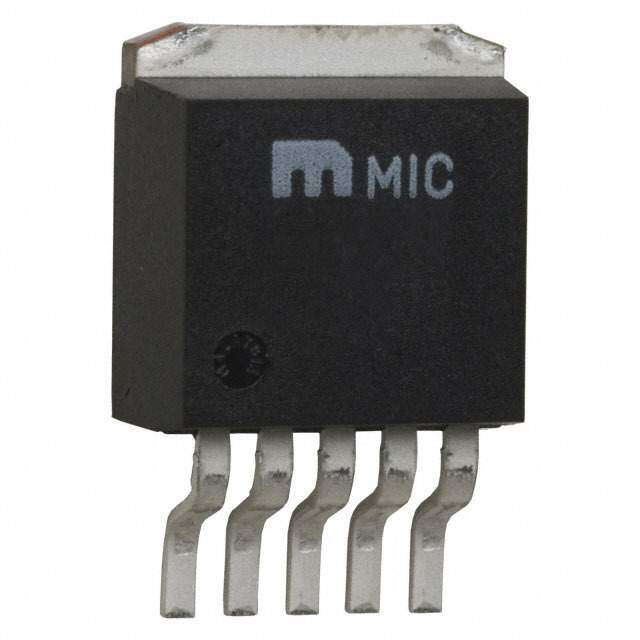
| 描述 | IC REG LDO 3.3V 1A DDPAK低压差稳压器 1A LDO REG |
| 产品分类 | |
| 品牌 | Texas Instruments |
| 产品手册 | |
| 产品图片 |
|
| rohs | 符合RoHS含铅 / 不受限制有害物质指令(RoHS)规范要求限制 |
| 产品系列 | 电源管理 IC,低压差稳压器,Texas Instruments LM3940ISX-3.3/NOPB- |
| 数据手册 | |
| 产品型号 | LM3940ISX-3.3/NOPB |
| 产品目录页面 | |
| 产品种类 | 低压差稳压器 |
| 供应商器件封装 | DDPAK/TO-263-3 |
| 其它名称 | LM3940ISX-3.3/NOPBTR |
| 包装 | 带卷 (TR) |
| 商标 | Texas Instruments |
| 回动电压—最大值 | 310 mV |
| 安装类型 | 表面贴装 |
| 安装风格 | SMD/SMT |
| 封装 | Reel |
| 封装/外壳 | TO-263-4,D²Pak(3 引线+接片),TO-263AA |
| 封装/箱体 | TO-263-3 |
| 工作温度 | -40°C ~ 125°C |
| 工厂包装数量 | 500 |
| 最大输入电压 | 7.5 V |
| 最小工作温度 | - 40 C |
| 标准包装 | 500 |
| 电压-跌落(典型值) | 0.5V @ 1A |
| 电压-输入 | 最高 7.5V |
| 电压-输出 | 3.3V |
| 电流-输出 | 1A |
| 电流-限制(最小值) | - |
| 稳压器拓扑 | 正,固定式 |
| 稳压器数 | 1 |
| 系列 | LM3940 |
| 设计资源 | http://www.digikey.com/product-highlights/cn/zh/texas-instruments-webench-design-center/3176 |
| 输出电流 | 1 A |


PDF Datasheet 数据手册内容提取
Product Order Technical Tools & Support & Folder Now Documents Software Community LM3940 SNVS114G–MAY1999–REVISEDFEBRUARY2015 LM3940 1-A Low-Dropout Regulator for 5-V to 3.3-V Conversion 1 Features 3 Description • InputVoltageRange:4.5Vto5.5V The LM3940 is a 1-A low-dropout regulator designed 1 toprovide3.3Vfroma5-Vsupply. • OutputVoltageSpecifiedoverTemperature The LM3940 is ideally suited for systems which • ExcellentLoadRegulation contain both 5-V and 3.3-V logic, with prime power • Specified1-AOutputCurrent providedfroma5-Vbus. • RequiresonlyOneExternalComponent Because the LM3940 is a true low dropout regulator, • Built-inProtectionagainstExcessTemperature it can hold its 3.3-V output in regulation with input • Short-CircuitProtected voltagesaslowas4.5V. The TO-220 package of the LM3940 means that in 2 Applications most applications the full 1 A of load current can be • LaptopandDesktopComputers deliveredwithoutusinganadditionalheatsink. • LogicSystems The surface mount DDPAK/TO-263 package uses minimum board space, and gives excellent power dissipation capability when soldered to a copper planeonthePCboard. DeviceInformation(1) PARTNUMBER PACKAGE BODYSIZE(NOM) SOT-223(4) 6.50mmx3.50mm LM3940 DDPAK/TO-263(3) 10.18mmx8.41mm TO-220(3) 14.986mmx10.16mm (1) For all available packages, see the orderable addendum at theendofthedatasheet. SimplifiedSchematic *Requiredifregulatorislocatedmorethan1inchfromthepowersupplyfiltercapacitororifbatterypowerisused. **SeeApplicationandImplementation. 1 An IMPORTANT NOTICE at the end of this data sheet addresses availability, warranty, changes, use in safety-critical applications, intellectualpropertymattersandotherimportantdisclaimers.PRODUCTIONDATA.
LM3940 SNVS114G–MAY1999–REVISEDFEBRUARY2015 www.ti.com Table of Contents 1 Features.................................................................. 1 8 ApplicationandImplementation.......................... 9 2 Applications........................................................... 1 8.1 ApplicationInformation..............................................9 3 Description............................................................. 1 8.2 TypicalApplication....................................................9 4 RevisionHistory..................................................... 2 9 PowerSupplyRecommendations...................... 11 5 PinConfigurationandFunctions......................... 3 10 Layout................................................................... 11 6 Specifications......................................................... 4 10.1 LayoutGuidelines.................................................11 6.1 AbsoluteMaximumRatings......................................4 10.2 LayoutExample....................................................11 6.2 ESDRatings..............................................................4 10.3 Heatsinking...........................................................11 6.3 RecommendedOperatingConditions.......................4 11 DeviceandDocumentationSupport................. 15 6.4 ThermalInformation..................................................4 11.1 DocumentationSupport........................................15 6.5 ElectricalCharacteristics...........................................5 11.2 ReceivingNotificationofDocumentationUpdates15 6.6 TypicalCharacteristics..............................................6 11.3 CommunityResources..........................................15 7 DetailedDescription.............................................. 8 11.4 Trademarks...........................................................15 7.1 Overview...................................................................8 11.5 ElectrostaticDischargeCaution............................15 7.2 FunctionalBlockDiagram.........................................8 11.6 Glossary................................................................15 7.3 FeatureDescription...................................................8 12 Mechanical,Packaging,andOrderable Information........................................................... 15 7.4 DeviceFunctionalModes..........................................8 4 Revision History NOTE:Pagenumbersforpreviousrevisionsmaydifferfrompagenumbersinthecurrentversion. ChangesfromRevisionF(November2014)toRevisionG Page • ChangedpinnamestoTInomenclature................................................................................................................................ 1 • DeletedsolderinginformationfromAbMax;thisinfoisinPOA ........................................................................................... 4 • ChangedHandlingRatingstabletoESDRatingstable;movestoragetemptoAbMax...................................................... 4 • ChangedvaluesinInputsupplyvoltagerow,ROCtable ...................................................................................................... 4 • ChangedI toI .................................................................................................................................................................. 5 L OUT ChangesfromRevisionE(March2013)toRevisionF Page • AddedDeviceInformationandHandlingRatingtables,FeatureDescription,DeviceFunctionalModes,Application andImplementation,PowerSupplyRecommendations,Layout,DeviceandDocumentationSupport,and Mechanical,Packaging,andOrderableInformationsections;movedsomecurvestoApplicationCurvessection; updatethermalvalues............................................................................................................................................................ 1 ChangesfromRevisionD(March2013)toRevisionE Page • ChangedlayoutofNationalDataSheettoTIformat........................................................................................................... 14 2 SubmitDocumentationFeedback Copyright©1999–2015,TexasInstrumentsIncorporated ProductFolderLinks:LM3940
LM3940 www.ti.com SNVS114G–MAY1999–REVISEDFEBRUARY2015 5 Pin Configuration and Functions 3-Pin TO-220Package 4-Pin FrontView SOT-223 FrontView 3-Pin DDPAK/TO-263Package FrontView PinFunctions PIN I/O DESCRIPTION NAME TO-220 TO-263 SOT-223 Inputvoltagesupply.A0.47-µFcapacitorshouldbeconnected IN 1 1 1 I atthisinput. GND 2 2 2,4 — Commonground Outputvoltage.A33-µFlowESRcapacitorshouldbe OUT 3 3 3 O connectedtothispin. Copyright©1999–2015,TexasInstrumentsIncorporated SubmitDocumentationFeedback 3 ProductFolderLinks:LM3940
LM3940 SNVS114G–MAY1999–REVISEDFEBRUARY2015 www.ti.com 6 Specifications 6.1 Absolute Maximum Ratings overoperatingfree-airtemperaturerange(unlessotherwisenoted)(1) MIN MAX UNIT Powerdissipation(2) Internally Limited Inputsupplyvoltage –0.3 7.5 V Storagetemperature,T −65 150 °C stg (1) StressesbeyondthoselistedunderAbsoluteMaximumRatingsmaycausepermanentdamagetothedevice.Thesearestressratings only,whichdonotimplyfunctionaloperationofthedeviceattheseoranyotherconditionsbeyondthoseindicatedunderRecommended OperatingConditions.Exposuretoabsolute-maximum-ratedconditionsforextendedperiodsmayaffectdevicereliability. (2) Themaximumallowablepowerdissipationisafunctionofthemaximumjunctiontemperature,T,thejunction-to-ambientthermal J resistance,R ,andtheambienttemperature,T .Exceedingthemaximumallowablepowerdissipationwillcauseexcessivedie θJA A temperature,andtheregulatorwillgointothermalshutdown.ThevalueofR (fordevicesinstillairwithnoheatsink)is23.3°C/Wfor θJA theTO-220package,40.9°C/WfortheDDPAK/TO-263package,and59.3°C/WfortheSOT-223package.TheeffectivevalueofR θJA canbereducedbyusingaheatsink(seeHeatsinkingforspecificinformationonheatsinking). 6.2 ESD Ratings VALUE UNIT Human-bodymodel(HBM),perANSI/ESDA/JEDECJS-001(1) ±2000 V(ESD) Electrostaticdischarge Charged-devicemodel(CDM),perJEDECspecificationJESD22- V C101(2) ±500 (1) JEDECdocumentJEP155statesthat500-VHBMallowssafemanufacturingwithastandardESDcontrolprocess. (2) JEDECdocumentJEP157statesthat250-VCDMallowssafemanufacturingwithastandardESDcontrolprocess. 6.3 Recommended Operating Conditions overoperatingfree-airtemperaturerange(unlessotherwisenoted) MIN MAX UNIT Junctiontemperature,T –40 125 °C J Inputsupplyvoltage,V 4.5 5.5 V IN 6.4 Thermal Information LM3940 THERMALMETRIC(1) SOT-223 TO-263(KTT) TO-220(NDE) UNIT (DCY) 4PINS 3PINS 3PINS R Junction-to-ambientthermalresistance,High-K 59.3 40.9 23.3 °C/W θJA R Junction-to-case(top)thermalresistance 38.9 43.5 16.1 °C/W θJC(top) R Junction-to-boardthermalresistance 8.1 23.5 4.8 °C/W θJB ψ Junction-to-topcharacterizationparameter 1.7 10.3 2.7 °C/W JT ψ Junction-to-boardcharacterizationparameter 8.0 22.5 4.8 °C/W JB R Junction-to-case(bottom)thermalresistance n/a 0.8 1.1 °C/W θJC(bot) (1) Formoreinformationabouttraditionalandnewthermalmetrics,seetheICPackageThermalMetricsapplicationreport,SPRA953. 4 SubmitDocumentationFeedback Copyright©1999–2015,TexasInstrumentsIncorporated ProductFolderLinks:LM3940
LM3940 www.ti.com SNVS114G–MAY1999–REVISEDFEBRUARY2015 6.5 Electrical Characteristics Overoperatingfree-airtemperaturerange,V =5V,I =1A,C =33μF(unlessotherwisenoted).LimitsapplyforT = IN OUT OUT J 25°C,unlessotherwisespecifiedintheTestConditionscolumn.(1) PARAMETER TESTCONDITIONS MIN TYP MAX UNIT 5mA≤I ≤1A,T =25°C 3.20 3.3 3.40 OUT J VOUT Outputvoltage 5mA≤IOUT≤1A, 3.13 3.47 V –40°C≤T ≤125°C J ßVOUT Lineregulation IOUT=5mA 20 40 ßVIN 4.5V≤VIN≤5.5V 50mA≤I ≤1A,T =25°C 35 50 mV OUT J ßßVIOOUUTT Loadregulation 50mA≤IOUT≤1A 35 80 –40°C≤T ≤125°C J I (DC)=100mA OUT Z Outputimpedance I (AC)=20mA(rms) 35 mΩ OUT OUT ƒ=120Hz 4.5V≤V ≤5.5V,I =5 IN OUT 10 15 mA,T =25°C J 4.5V≤V ≤5.5V,I =5 IN OUT mA 10 20 IQ Quiescentcurrent –40°C≤TJ≤125°C mA V =5V,I =1A,T = IN OUT J 110 200 25°C V =5V,I =1A IN OUT 110 250 –40°C≤T ≤125°C J ƒ =10Hz–100kHz e Outputnoisevoltage BW 150 μV n I =5mA (rms) OUT I =1A,T =25°C 0.5 0.8 OUT J I =1A V OUT 0.5 1 –40°C≤T ≤125°C V Dropoutvoltage(2) J DO I =100mA,T =25°C 110 150 OUT J I =100mA mV OUT 110 200 –40°C≤T ≤125°C J I Short-circuitcurrent R =0 1.2 1.7 A OUT(SC) L (1) AlllimitsspecifiedforT =25°Care100%testedandareusedtocalculateOutgoingQualityLevels.Alllimitsattemperatureextremes J areverifiedviacorrelationusingstandardStatisticalQualityControl(SQC)methods. (2) Dropoutvoltageisdefinedastheinput-outputdifferentialvoltagewheretheregulatoroutputdropstoavaluethatis100mVbelowthe valuethatismeasuredatV =5V. IN Copyright©1999–2015,TexasInstrumentsIncorporated SubmitDocumentationFeedback 5 ProductFolderLinks:LM3940
LM3940 SNVS114G–MAY1999–REVISEDFEBRUARY2015 www.ti.com 6.6 Typical Characteristics AtT =25°C,unlessotherwisenoted. J Figure1.DropoutVoltage Figure2.DropoutVoltagevs.Temperature Figure3.OutputVoltagevs.Temperature Figure4.QuiescentCurrentvs.Temperature Figure5.QuiescentCurrentvs.V Figure6.QuiescentCurrentvs.Load IN 6 SubmitDocumentationFeedback Copyright©1999–2015,TexasInstrumentsIncorporated ProductFolderLinks:LM3940
LM3940 www.ti.com SNVS114G–MAY1999–REVISEDFEBRUARY2015 Typical Characteristics (continued) AtT =25°C,unlessotherwisenoted. J Figure7.RippleRejection Figure8.OutputImpedance Figure9.PeakOutputCurrent Figure10.LowVoltageBehavior Copyright©1999–2015,TexasInstrumentsIncorporated SubmitDocumentationFeedback 7 ProductFolderLinks:LM3940
LM3940 SNVS114G–MAY1999–REVISEDFEBRUARY2015 www.ti.com 7 Detailed Description 7.1 Overview The LM3940 is a low dropout regulator capable of sourcing a 1-A load. The LM3940 provides 3.3 V from 5-V supply. LM3940 is ideally suited for system which contain both 5-V and 3.3-V logic, with prime power provided froma5-Vbus. 7.2 Functional Block Diagram IN OUT OVSD Current Thermal PNP (§(cid:3)30V) Limit Shutdown + Bandgap Reference GND 7.3 Feature Description 7.3.1 OutputVoltageAccuracy Output voltage accuracy specifies minimum and maximum output voltage error, relative to the expected nominal output voltage. This accuracy error includes the errors introduced by line and load regulation across the full rangeofratedloadandlineoperatingconditions,unlessotherwisespecifiedbytheElectricalCharacteristics. 7.3.2 Short-CircuitProtection The internal current limit circuit is used to protect the LDO against high-load current faults or shorting events. During a current-limit event, the LDO sources constant current. Therefore, the output voltage falls when load impedance decreases. Note also that if a current limit occurs and the resulting output voltage is low, excessive powermaybedissipatedacrosstheLDO,resultinginathermalshutdownoftheoutput. 7.3.3 ThermalProtection The LM3940 contains a thermal shutdown protection circuit to turn off the output current when excessive heat is dissipated in the LDO. The thermal time-constant of the semiconductor die is fairly short, and thus the output cyclesonandoffatahighratewhenthermalshutdownisreacheduntilthepowerdissipationisreduced. The internal protection circuit of LM3940 is designed to protect against thermal overload conditions. The circuit is not intended to replace proper heat sinking. Continuously running the device into thermal shutdown degrades its reliability. 7.4 Device Functional Modes 7.4.1 OperationwithV =5V IN The device operates at input voltage is 5 V and output voltage is 3.3 V. The LM3940 is a true low dropout regulator,itcanholdits3.3-Voutputinregulationwithinputvoltagesaslowas4.5V. 8 SubmitDocumentationFeedback Copyright©1999–2015,TexasInstrumentsIncorporated ProductFolderLinks:LM3940
LM3940 www.ti.com SNVS114G–MAY1999–REVISEDFEBRUARY2015 8 Application and Implementation NOTE Information in the following applications sections is not part of the TI component specification, and TI does not warrant its accuracy or completeness. TI’s customers are responsible for determining suitability of components for their purposes. Customers should validateandtesttheirdesignimplementationtoconfirmsystemfunctionality. 8.1 Application Information The LM3940 is a linear voltage regulator operating from 5 V on the input and regulates voltage to 3.3V with 1-A maximum output current. This device is suited for system which contain both 5-V and 3.3-V logic, with prime powerprovidedfroma5-Vbus. 8.2 Typical Application *Requiredifregulatorislocatedmorethan1″fromthepowersupplyfiltercapacitororifbatterypowerisused. **SeeDetailedDesignProcedure. Figure11. TypicalApplication 8.2.1 DesignRequirements DESIGNPARAMETER EXAMPLEVALUE Inputvoltage 5V,±10% Outputvoltage 3.3V,±3% Outputcurrent 1A 8.2.2 DetailedDesignProcedure 8.2.2.1 ExternalCapacitors The output capacitor is critical to maintaining regulator stability, and must meet the required conditions for both equivalentseriesresistance(ESR)andminimumamountofcapacitance. 8.2.2.1.1 MinimumCapacitance The minimum output capacitance required to maintain stability is 33 μF (this value may be increased without limit).Largervaluesofoutputcapacitancewillgiveimprovedtransientresponse. 8.2.2.1.2 ESRLimits The ESR of the output capacitor will cause loop instability if it is too high or too low. The acceptable range of ESR plotted versus load current is shown in Figure 12. It is essential that the output capacitor meet these requirements,oroscillationscanresult. Copyright©1999–2015,TexasInstrumentsIncorporated SubmitDocumentationFeedback 9 ProductFolderLinks:LM3940
LM3940 SNVS114G–MAY1999–REVISEDFEBRUARY2015 www.ti.com Figure12. ESRLimits Itisimportanttonotethatformostcapacitors,ESRisspecifiedonlyatroomtemperature.However,thedesigner must ensure that the ESR will stay inside the limits shown over the entire operating temperature range for the design. Foraluminumelectrolyticcapacitors,ESRwillincreasebyabout30Xasthetemperatureisreducedfrom25°Cto −40°C.Thistypeofcapacitorisnotwell-suitedforlowtemperatureoperation. Solid tantalum capacitors have a more stable ESR over temperature, but are more expensive than aluminum electrolytics. A cost-effective approach sometimes used is to parallel an aluminum electrolytic with a solid tantalum,withthetotalcapacitancesplitabout75/25%withthealuminumbeingthelargervalue. If two capacitors are paralleled, the effective ESR is the parallel of the two individual values. The “flatter” ESR of theTantalumwillkeeptheeffectiveESRfromrisingasquicklyatlowtemperatures. 8.2.3 ApplicationCurves Figure13.LineTransientResponse Figure14.LoadTransientResponse 10 SubmitDocumentationFeedback Copyright©1999–2015,TexasInstrumentsIncorporated ProductFolderLinks:LM3940
LM3940 www.ti.com SNVS114G–MAY1999–REVISEDFEBRUARY2015 9 Power Supply Recommendations TheLM3940isdesignedtooperatefroman5-Vinputvoltagesupply.Thisinputsupplymustbewellregulated.If the input supply is noisy, additional input capacitors with low ESR can help improve the output noise performance. 10 Layout 10.1 Layout Guidelines For best overall performance, place all the circuit components on the same side of the circuit board and as near as practical to the respective LDO pin connections. Place ground return connections to the input and output capacitor, and to the LDO ground pin as close to each other as possible, connected by a wide, component-side, copper surface. The use of vias and long traces to create LDO circuit connections is strongly discouraged and negatively affects system performance. This grounding and layout scheme minimizes inductive parasitic, and therebyreducesload-currenttransients,minimizesnoise,andincreasescircuitstability. A ground reference plane is also recommended and is either embedded in the PCB itself or located on the bottom side of the PCB opposite the components. This reference plane serves to assure accuracy of the output voltage, shield noise, and behaves similar to a thermal plane to spread heat from the LDO device. In most applications,thisgroundplaneisnecessarytomeetthermalrequirements. 10.2 Layout Example 4 (TAB) VIN VOUT 1 2 3 IN D OUT N G GND Figure15. LM3940LayoutExample 10.3 Heatsinking Aheatsinkmayberequireddependingonthemaximumpowerdissipationandmaximumambienttemperatureof the application. Under all possible operating conditions, the junction temperature must be within the range specifiedunderAbsoluteMaximumRatings. Todetermineifaheatsinkisrequired,thepowerdissipatedbytheregulator,P ,mustbecalculated. D Figure 16 shows the voltages and currents which are present in the circuit, as well as the formula for calculating thepowerdissipatedintheregulator: Copyright©1999–2015,TexasInstrumentsIncorporated SubmitDocumentationFeedback 11 ProductFolderLinks:LM3940
LM3940 SNVS114G–MAY1999–REVISEDFEBRUARY2015 www.ti.com Heatsinking (continued) I =I +I IN OUT G P =(V −V )I +(V )I D IN OUT OUT IN G Figure16. PowerDissipationDiagram The next parameter which must be calculated is the maximum allowable temperature rise, T (max). This is R calculatedbyusingtheformula: T (max)=T (max)−T (max) R J A Where:T (max)isthemaximumallowablejunctiontemperature,whichis125°Cforcommercialgradeparts. J T (max)isthemaximumambienttemperaturewhichwillbeencounteredintheapplication. A Using the calculated values for T (max) and P , the maximum allowable value for the junction-to-ambient R D thermalresistance,R ,cannowbefound: θ(JA) R =T (max)/P θ(JA) R D IMPORTANT: If the maximum allowable value for θ is found to be ≥ 23.3°C/W for the TO-220 package, ≥ (JA) 40.9°C/W for the DDPAK/TO-263 package, or ≥59.3°C/W for the SOT-223 package, no heatsink is needed since thepackagealonewilldissipateenoughheattosatisfytheserequirements. Ifthecalculatedvalueforθ fallsbelowtheselimits,aheatsinkisrequired. (JA) 10.3.1 HeatsinkingTO-220PackageParts TheTO-220canbeattachedtoatypicalheatsink,orsecuredtoacopperplaneonaPCboard.Ifacopperplane is to be used, the values of R will be the same as shown in the Heatsinking DDPAK/TO-263 and SOT-223 θ(JA) PackagePartssectionfortheDDPAK/TO-263. If a manufactured heatsink is to be selected, the value of heatsink-to-ambient thermal resistance, R , must θ(H−A) firstbecalculated: R =R − R −R θ(H−A) θ(JA) θ(C−H) θ(J−C) Where:R isdefinedasthethermalresistancefromthejunctiontothesurfaceofthecase.Avalueof4°C/W θ(J−C) canbeassumedforθ forthiscalculation. (J−C) R isdefinedasthethermalresistancebetweenthecaseandthesurfaceoftheheatsink.Thevalueof θ(C−H) θ willvaryfromabout1.5°C/Wtoabout2.5°C/W(dependingonmethodofattachment, (C−H) insulator,etc.).Iftheexactvalueisunknown,2°C/Wshouldbeassumedfor θ . (C−H) When a value for R is found using the equation shown above, a heatsink must be selected that has a value θ(H−A) thatislessthanorequaltothisnumber. R is specified numerically by the heatsink manufacturer in the catalog, or shown in a curve that plots θ(H−A) temperaturerisevs.powerdissipationfortheheatsink. 10.3.2 HeatsinkingDDPAK/TO-263andSOT-223PackageParts Both the DDPAK/TO-263 (KTT) and SOT-223 (DCY) packages use a copper plane on the PCB and the PCB itself as a heatsink. To optimize the heat sinking ability of the plane and PCB, solder the tab of the package to theplane. Figure 17 shows for the DDPAK/TO-263 the measured values of R for different copper area sizes using a θ(JA) typicalPCBwith1ouncecopperandnosoldermaskoverthecopperareausedforheatsinking. 12 SubmitDocumentationFeedback Copyright©1999–2015,TexasInstrumentsIncorporated ProductFolderLinks:LM3940
LM3940 www.ti.com SNVS114G–MAY1999–REVISEDFEBRUARY2015 Heatsinking (continued) Figure17. R vs.Copper(1ounce)AreafortheDDPAK/TO-263Package θ(JA) As shown in Figure 17, increasing the copper area beyond 1 square inch produces very little improvement. It should also be observed that the minimum value of R for the DDPAK/TO-263 package mounted to a PCB is θ(JA) 32°C/W. As a design aid, Figure 18 shows the maximum allowable power dissipation compared to ambient temperature fortheDDPAK/TO-263device(assumingR is35°C/Wandthemaximumjunctiontemperatureis125°C). θ(JA) Figure18. MaximumPowerDissipationvs.T fortheDDPAK/TO-263Package AMB Figure 19 and Figure 20 show the information for the SOT-223 package. Figure 20 assumes a R of 74°C/W θ(JA) for1ouncecopperand51°C/Wfor2ouncecopperandamaximumjunctiontemperatureof125°C. Figure19. R vs.Copper(2ounce)AreafortheSOT-223Package θ(JA) Copyright©1999–2015,TexasInstrumentsIncorporated SubmitDocumentationFeedback 13 ProductFolderLinks:LM3940
LM3940 SNVS114G–MAY1999–REVISEDFEBRUARY2015 www.ti.com Heatsinking (continued) Figure20. MaximumPowerDissipationvs.T fortheSOT-223Package AMB Please see AN-1028 Maximum Power Enhancement Techniques for Power Packages, SNVA036 for power enhancementtechniquestobeusedwiththeSOT-223package. 14 SubmitDocumentationFeedback Copyright©1999–2015,TexasInstrumentsIncorporated ProductFolderLinks:LM3940
LM3940 www.ti.com SNVS114G–MAY1999–REVISEDFEBRUARY2015 11 Device and Documentation Support 11.1 Documentation Support 11.1.1 RelatedDocumentation Forrelateddocumentationseethefollowing: AN-1028MaximumPowerEnhancementTechniquesforPowerPackages,SNVA036 11.2 Receiving Notification of Documentation Updates To receive notification of documentation updates, navigate to the device product folder on ti.com. In the upper right corner, click on Alert me to register and receive a weekly digest of any product information that has changed.Forchangedetails,reviewtherevisionhistoryincludedinanyreviseddocument. 11.3 Community Resources The following links connect to TI community resources. Linked contents are provided "AS IS" by the respective contributors. They do not constitute TI specifications and do not necessarily reflect TI's views; see TI's Terms of Use. TIE2E™OnlineCommunity TI'sEngineer-to-Engineer(E2E)Community.Createdtofostercollaboration amongengineers.Ate2e.ti.com,youcanaskquestions,shareknowledge,exploreideasandhelp solveproblemswithfellowengineers. DesignSupport TI'sDesignSupport QuicklyfindhelpfulE2Eforumsalongwithdesignsupporttoolsand contactinformationfortechnicalsupport. 11.4 Trademarks E2EisatrademarkofTexasInstruments. Allothertrademarksarethepropertyoftheirrespectiveowners. 11.5 Electrostatic Discharge Caution Thesedeviceshavelimitedbuilt-inESDprotection.Theleadsshouldbeshortedtogetherorthedeviceplacedinconductivefoam duringstorageorhandlingtopreventelectrostaticdamagetotheMOSgates. 11.6 Glossary SLYZ022—TIGlossary. Thisglossarylistsandexplainsterms,acronyms,anddefinitions. 12 Mechanical, Packaging, and Orderable Information The following pages include mechanical, packaging, and orderable information. This information is the most current data available for the designated devices. This data is subject to change without notice and revision of thisdocument.Forbrowser-basedversionsofthisdatasheet,refertotheleft-handnavigation. Copyright©1999–2015,TexasInstrumentsIncorporated SubmitDocumentationFeedback 15 ProductFolderLinks:LM3940
PACKAGE OPTION ADDENDUM www.ti.com 13-Feb-2015 PACKAGING INFORMATION Orderable Device Status Package Type Package Pins Package Eco Plan Lead/Ball Finish MSL Peak Temp Op Temp (°C) Device Marking Samples (1) Drawing Qty (2) (6) (3) (4/5) LM3940IMP-3.3 NRND SOT-223 DCY 4 1000 TBD Call TI Call TI -40 to 125 L52B LM3940IMP-3.3/NOPB ACTIVE SOT-223 DCY 4 1000 Green (RoHS CU SN Level-1-260C-UNLIM -40 to 125 L52B & no Sb/Br) LM3940IMPX-3.3 NRND SOT-223 DCY 4 2000 TBD Call TI Call TI -40 to 125 L52B LM3940IMPX-3.3/NOPB ACTIVE SOT-223 DCY 4 2000 Green (RoHS CU SN Level-1-260C-UNLIM -40 to 125 L52B & no Sb/Br) LM3940IS-3.3 NRND DDPAK/ KTT 3 45 TBD Call TI Call TI -40 to 125 LM3940IS TO-263 -3.3 P+ LM3940IS-3.3/NOPB ACTIVE DDPAK/ KTT 3 45 Pb-Free (RoHS CU SN Level-3-245C-168 HR -40 to 125 LM3940IS TO-263 Exempt) -3.3 P+ LM3940ISX-3.3 NRND DDPAK/ KTT 3 500 TBD Call TI Call TI -40 to 125 LM3940IS TO-263 -3.3 P+ LM3940ISX-3.3/NOPB ACTIVE DDPAK/ KTT 3 500 Pb-Free (RoHS CU SN Level-3-245C-168 HR -40 to 125 LM3940IS TO-263 Exempt) -3.3 P+ LM3940IT-3.3 NRND TO-220 NDE 3 45 TBD Call TI Call TI -40 to 125 LM3940IT -3.3 P+ LM3940IT-3.3/NOPB ACTIVE TO-220 NDE 3 45 Green (RoHS CU SN Level-1-NA-UNLIM -40 to 125 LM3940IT & no Sb/Br) -3.3 P+ (1) The marketing status values are defined as follows: ACTIVE: Product device recommended for new designs. LIFEBUY: TI has announced that the device will be discontinued, and a lifetime-buy period is in effect. NRND: Not recommended for new designs. Device is in production to support existing customers, but TI does not recommend using this part in a new design. PREVIEW: Device has been announced but is not in production. Samples may or may not be available. OBSOLETE: TI has discontinued the production of the device. (2) Eco Plan - The planned eco-friendly classification: Pb-Free (RoHS), Pb-Free (RoHS Exempt), or Green (RoHS & no Sb/Br) - please check http://www.ti.com/productcontent for the latest availability information and additional product content details. TBD: The Pb-Free/Green conversion plan has not been defined. Pb-Free (RoHS): TI's terms "Lead-Free" or "Pb-Free" mean semiconductor products that are compatible with the current RoHS requirements for all 6 substances, including the requirement that lead not exceed 0.1% by weight in homogeneous materials. Where designed to be soldered at high temperatures, TI Pb-Free products are suitable for use in specified lead-free processes. Pb-Free (RoHS Exempt): This component has a RoHS exemption for either 1) lead-based flip-chip solder bumps used between the die and package, or 2) lead-based die adhesive used between the die and leadframe. The component is otherwise considered Pb-Free (RoHS compatible) as defined above. Green (RoHS & no Sb/Br): TI defines "Green" to mean Pb-Free (RoHS compatible), and free of Bromine (Br) and Antimony (Sb) based flame retardants (Br or Sb do not exceed 0.1% by weight in homogeneous material) Addendum-Page 1
PACKAGE OPTION ADDENDUM www.ti.com 13-Feb-2015 (3) MSL, Peak Temp. - The Moisture Sensitivity Level rating according to the JEDEC industry standard classifications, and peak solder temperature. (4) There may be additional marking, which relates to the logo, the lot trace code information, or the environmental category on the device. (5) Multiple Device Markings will be inside parentheses. Only one Device Marking contained in parentheses and separated by a "~" will appear on a device. If a line is indented then it is a continuation of the previous line and the two combined represent the entire Device Marking for that device. (6) Lead/Ball Finish - Orderable Devices may have multiple material finish options. Finish options are separated by a vertical ruled line. Lead/Ball Finish values may wrap to two lines if the finish value exceeds the maximum column width. Important Information and Disclaimer:The information provided on this page represents TI's knowledge and belief as of the date that it is provided. TI bases its knowledge and belief on information provided by third parties, and makes no representation or warranty as to the accuracy of such information. Efforts are underway to better integrate information from third parties. TI has taken and continues to take reasonable steps to provide representative and accurate information but may not have conducted destructive testing or chemical analysis on incoming materials and chemicals. TI and TI suppliers consider certain information to be proprietary, and thus CAS numbers and other limited information may not be available for release. In no event shall TI's liability arising out of such information exceed the total purchase price of the TI part(s) at issue in this document sold by TI to Customer on an annual basis. Addendum-Page 2
PACKAGE MATERIALS INFORMATION www.ti.com 14-Feb-2015 TAPE AND REEL INFORMATION *Alldimensionsarenominal Device Package Package Pins SPQ Reel Reel A0 B0 K0 P1 W Pin1 Type Drawing Diameter Width (mm) (mm) (mm) (mm) (mm) Quadrant (mm) W1(mm) LM3940IMP-3.3 SOT-223 DCY 4 1000 330.0 16.4 7.0 7.5 2.2 12.0 16.0 Q3 LM3940IMP-3.3/NOPB SOT-223 DCY 4 1000 330.0 16.4 7.0 7.5 2.2 12.0 16.0 Q3 LM3940IMPX-3.3 SOT-223 DCY 4 2000 330.0 16.4 7.0 7.5 2.2 12.0 16.0 Q3 LM3940IMPX-3.3/NOPB SOT-223 DCY 4 2000 330.0 16.4 7.0 7.5 2.2 12.0 16.0 Q3 LM3940ISX-3.3 DDPAK/ KTT 3 500 330.0 24.4 10.75 14.85 5.0 16.0 24.0 Q2 TO-263 LM3940ISX-3.3/NOPB DDPAK/ KTT 3 500 330.0 24.4 10.75 14.85 5.0 16.0 24.0 Q2 TO-263 PackMaterials-Page1
PACKAGE MATERIALS INFORMATION www.ti.com 14-Feb-2015 *Alldimensionsarenominal Device PackageType PackageDrawing Pins SPQ Length(mm) Width(mm) Height(mm) LM3940IMP-3.3 SOT-223 DCY 4 1000 367.0 367.0 35.0 LM3940IMP-3.3/NOPB SOT-223 DCY 4 1000 367.0 367.0 35.0 LM3940IMPX-3.3 SOT-223 DCY 4 2000 367.0 367.0 35.0 LM3940IMPX-3.3/NOPB SOT-223 DCY 4 2000 367.0 367.0 35.0 LM3940ISX-3.3 DDPAK/TO-263 KTT 3 500 367.0 367.0 45.0 LM3940ISX-3.3/NOPB DDPAK/TO-263 KTT 3 500 367.0 367.0 45.0 PackMaterials-Page2
MECHANICAL DATA NDE0003B www.ti.com
MECHANICAL DATA MPDS094A – APRIL 2001 – REVISED JUNE 2002 DCY (R-PDSO-G4) PLASTIC SMALL-OUTLINE 6,70 (0.264) 6,30 (0.248) 3,10 (0.122) 2,90 (0.114) 4 0,10 (0.004) M 7,30 (0.287) 3,70 (0.146) 6,70 (0.264) 3,30 (0.130) Gauge Plane 1 2 3 0,84 (0.033) 0°–10° 0,25 (0.010) 2,30 (0.091) 0,66 (0.026) 0,10 (0.004) M 4,60 (0.181) 0,75 (0.030) MIN 1,70 (0.067) 1,80 (0.071) MAX 1,50 (0.059) 0,35 (0.014) 0,23 (0.009) Seating Plane 0,10 (0.0040) 0,08 (0.003) 0,02 (0.0008) 4202506/B 06/2002 NOTES: A. All linear dimensions are in millimeters (inches). B. This drawing is subject to change without notice. C. Body dimensions do not include mold flash or protrusion. D. Falls within JEDEC TO-261 Variation AA. • POST OFFICE BOX 655303 DALLAS, TEXAS 75265
None
MECHANICAL DATA KTT0003B TS3B (Rev F) BOTTOM SIDE OF PACKAGE www.ti.com
IMPORTANTNOTICE TexasInstrumentsIncorporated(TI)reservestherighttomakecorrections,enhancements,improvementsandotherchangestoits semiconductorproductsandservicesperJESD46,latestissue,andtodiscontinueanyproductorserviceperJESD48,latestissue.Buyers shouldobtainthelatestrelevantinformationbeforeplacingordersandshouldverifythatsuchinformationiscurrentandcomplete. TI’spublishedtermsofsaleforsemiconductorproducts(http://www.ti.com/sc/docs/stdterms.htm)applytothesaleofpackagedintegrated circuitproductsthatTIhasqualifiedandreleasedtomarket.AdditionaltermsmayapplytotheuseorsaleofothertypesofTIproductsand services. ReproductionofsignificantportionsofTIinformationinTIdatasheetsispermissibleonlyifreproductioniswithoutalterationandis accompaniedbyallassociatedwarranties,conditions,limitations,andnotices.TIisnotresponsibleorliableforsuchreproduced documentation.Informationofthirdpartiesmaybesubjecttoadditionalrestrictions.ResaleofTIproductsorserviceswithstatements differentfromorbeyondtheparametersstatedbyTIforthatproductorservicevoidsallexpressandanyimpliedwarrantiesforthe associatedTIproductorserviceandisanunfairanddeceptivebusinesspractice.TIisnotresponsibleorliableforanysuchstatements. BuyersandotherswhoaredevelopingsystemsthatincorporateTIproducts(collectively,“Designers”)understandandagreethatDesigners remainresponsibleforusingtheirindependentanalysis,evaluationandjudgmentindesigningtheirapplicationsandthatDesignershave fullandexclusiveresponsibilitytoassurethesafetyofDesigners'applicationsandcomplianceoftheirapplications(andofallTIproducts usedinorforDesigners’applications)withallapplicableregulations,lawsandotherapplicablerequirements.Designerrepresentsthat,with respecttotheirapplications,Designerhasallthenecessaryexpertisetocreateandimplementsafeguardsthat(1)anticipatedangerous consequencesoffailures,(2)monitorfailuresandtheirconsequences,and(3)lessenthelikelihoodoffailuresthatmightcauseharmand takeappropriateactions.DesigneragreesthatpriortousingordistributinganyapplicationsthatincludeTIproducts,Designerwill thoroughlytestsuchapplicationsandthefunctionalityofsuchTIproductsasusedinsuchapplications. TI’sprovisionoftechnical,applicationorotherdesignadvice,qualitycharacterization,reliabilitydataorotherservicesorinformation, including,butnotlimitedto,referencedesignsandmaterialsrelatingtoevaluationmodules,(collectively,“TIResources”)areintendedto assistdesignerswhoaredevelopingapplicationsthatincorporateTIproducts;bydownloading,accessingorusingTIResourcesinany way,Designer(individuallyor,ifDesignerisactingonbehalfofacompany,Designer’scompany)agreestouseanyparticularTIResource solelyforthispurposeandsubjecttothetermsofthisNotice. TI’sprovisionofTIResourcesdoesnotexpandorotherwisealterTI’sapplicablepublishedwarrantiesorwarrantydisclaimersforTI products,andnoadditionalobligationsorliabilitiesarisefromTIprovidingsuchTIResources.TIreservestherighttomakecorrections, enhancements,improvementsandotherchangestoitsTIResources.TIhasnotconductedanytestingotherthanthatspecifically describedinthepublisheddocumentationforaparticularTIResource. Designerisauthorizedtouse,copyandmodifyanyindividualTIResourceonlyinconnectionwiththedevelopmentofapplicationsthat includetheTIproduct(s)identifiedinsuchTIResource.NOOTHERLICENSE,EXPRESSORIMPLIED,BYESTOPPELOROTHERWISE TOANYOTHERTIINTELLECTUALPROPERTYRIGHT,ANDNOLICENSETOANYTECHNOLOGYORINTELLECTUALPROPERTY RIGHTOFTIORANYTHIRDPARTYISGRANTEDHEREIN,includingbutnotlimitedtoanypatentright,copyright,maskworkright,or otherintellectualpropertyrightrelatingtoanycombination,machine,orprocessinwhichTIproductsorservicesareused.Information regardingorreferencingthird-partyproductsorservicesdoesnotconstitutealicensetousesuchproductsorservices,orawarrantyor endorsementthereof.UseofTIResourcesmayrequirealicensefromathirdpartyunderthepatentsorotherintellectualpropertyofthe thirdparty,oralicensefromTIunderthepatentsorotherintellectualpropertyofTI. TIRESOURCESAREPROVIDED“ASIS”ANDWITHALLFAULTS.TIDISCLAIMSALLOTHERWARRANTIESOR REPRESENTATIONS,EXPRESSORIMPLIED,REGARDINGRESOURCESORUSETHEREOF,INCLUDINGBUTNOTLIMITEDTO ACCURACYORCOMPLETENESS,TITLE,ANYEPIDEMICFAILUREWARRANTYANDANYIMPLIEDWARRANTIESOF MERCHANTABILITY,FITNESSFORAPARTICULARPURPOSE,ANDNON-INFRINGEMENTOFANYTHIRDPARTYINTELLECTUAL PROPERTYRIGHTS.TISHALLNOTBELIABLEFORANDSHALLNOTDEFENDORINDEMNIFYDESIGNERAGAINSTANYCLAIM, INCLUDINGBUTNOTLIMITEDTOANYINFRINGEMENTCLAIMTHATRELATESTOORISBASEDONANYCOMBINATIONOF PRODUCTSEVENIFDESCRIBEDINTIRESOURCESOROTHERWISE.INNOEVENTSHALLTIBELIABLEFORANYACTUAL, DIRECT,SPECIAL,COLLATERAL,INDIRECT,PUNITIVE,INCIDENTAL,CONSEQUENTIALOREXEMPLARYDAMAGESIN CONNECTIONWITHORARISINGOUTOFTIRESOURCESORUSETHEREOF,ANDREGARDLESSOFWHETHERTIHASBEEN ADVISEDOFTHEPOSSIBILITYOFSUCHDAMAGES. UnlessTIhasexplicitlydesignatedanindividualproductasmeetingtherequirementsofaparticularindustrystandard(e.g.,ISO/TS16949 andISO26262),TIisnotresponsibleforanyfailuretomeetsuchindustrystandardrequirements. WhereTIspecificallypromotesproductsasfacilitatingfunctionalsafetyorascompliantwithindustryfunctionalsafetystandards,such productsareintendedtohelpenablecustomerstodesignandcreatetheirownapplicationsthatmeetapplicablefunctionalsafetystandards andrequirements.Usingproductsinanapplicationdoesnotbyitselfestablishanysafetyfeaturesintheapplication.Designersmust ensurecompliancewithsafety-relatedrequirementsandstandardsapplicabletotheirapplications.DesignermaynotuseanyTIproductsin life-criticalmedicalequipmentunlessauthorizedofficersofthepartieshaveexecutedaspecialcontractspecificallygoverningsuchuse. Life-criticalmedicalequipmentismedicalequipmentwherefailureofsuchequipmentwouldcauseseriousbodilyinjuryordeath(e.g.,life support,pacemakers,defibrillators,heartpumps,neurostimulators,andimplantables).Suchequipmentincludes,withoutlimitation,all medicaldevicesidentifiedbytheU.S.FoodandDrugAdministrationasClassIIIdevicesandequivalentclassificationsoutsidetheU.S. TImayexpresslydesignatecertainproductsascompletingaparticularqualification(e.g.,Q100,MilitaryGrade,orEnhancedProduct). Designersagreethatithasthenecessaryexpertisetoselecttheproductwiththeappropriatequalificationdesignationfortheirapplications andthatproperproductselectionisatDesigners’ownrisk.Designersaresolelyresponsibleforcompliancewithalllegalandregulatory requirementsinconnectionwithsuchselection. DesignerwillfullyindemnifyTIanditsrepresentativesagainstanydamages,costs,losses,and/orliabilitiesarisingoutofDesigner’snon- compliancewiththetermsandprovisionsofthisNotice. MailingAddress:TexasInstruments,PostOfficeBox655303,Dallas,Texas75265 Copyright©2017,TexasInstrumentsIncorporated